EP0607936A1 - Elektrisches Übergangsbauelement mit leichtdotiertem Buffergebiet zur präzisen Lokalisierung eines pn-Überganges - Google Patents
Elektrisches Übergangsbauelement mit leichtdotiertem Buffergebiet zur präzisen Lokalisierung eines pn-Überganges Download PDFInfo
- Publication number
- EP0607936A1 EP0607936A1 EP94100700A EP94100700A EP0607936A1 EP 0607936 A1 EP0607936 A1 EP 0607936A1 EP 94100700 A EP94100700 A EP 94100700A EP 94100700 A EP94100700 A EP 94100700A EP 0607936 A1 EP0607936 A1 EP 0607936A1
- Authority
- EP
- European Patent Office
- Prior art keywords
- doped
- buffer
- emitter
- base
- superlattice
- Prior art date
- Legal status (The legal status is an assumption and is not a legal conclusion. Google has not performed a legal analysis and makes no representation as to the accuracy of the status listed.)
- Withdrawn
Links
- 239000000463 material Substances 0.000 claims abstract description 109
- 239000002019 doping agent Substances 0.000 claims abstract description 68
- 238000009792 diffusion process Methods 0.000 claims abstract description 40
- 239000004065 semiconductor Substances 0.000 claims abstract description 23
- 230000003247 decreasing effect Effects 0.000 claims description 4
- 229910052790 beryllium Inorganic materials 0.000 claims description 2
- ATBAMAFKBVZNFJ-UHFFFAOYSA-N beryllium atom Chemical compound [Be] ATBAMAFKBVZNFJ-UHFFFAOYSA-N 0.000 claims description 2
- 229910000530 Gallium indium arsenide Inorganic materials 0.000 description 21
- GPXJNWSHGFTCBW-UHFFFAOYSA-N Indium phosphide Chemical compound [In]#P GPXJNWSHGFTCBW-UHFFFAOYSA-N 0.000 description 9
- 229910001218 Gallium arsenide Inorganic materials 0.000 description 7
- 238000001451 molecular beam epitaxy Methods 0.000 description 5
- 230000008859 change Effects 0.000 description 4
- 230000000694 effects Effects 0.000 description 4
- 238000004519 manufacturing process Methods 0.000 description 4
- 238000000034 method Methods 0.000 description 4
- 239000000758 substrate Substances 0.000 description 4
- 229910000980 Aluminium gallium arsenide Inorganic materials 0.000 description 3
- OKTJSMMVPCPJKN-UHFFFAOYSA-N Carbon Chemical compound [C] OKTJSMMVPCPJKN-UHFFFAOYSA-N 0.000 description 3
- 229910052799 carbon Inorganic materials 0.000 description 3
- 238000002347 injection Methods 0.000 description 3
- 239000007924 injection Substances 0.000 description 3
- 238000001004 secondary ion mass spectrometry Methods 0.000 description 3
- 230000003213 activating effect Effects 0.000 description 2
- 230000004888 barrier function Effects 0.000 description 2
- 230000008901 benefit Effects 0.000 description 2
- 230000015556 catabolic process Effects 0.000 description 2
- 238000006731 degradation reaction Methods 0.000 description 2
- 230000001419 dependent effect Effects 0.000 description 2
- 238000010586 diagram Methods 0.000 description 2
- 230000007246 mechanism Effects 0.000 description 2
- 229910052751 metal Inorganic materials 0.000 description 2
- 239000002184 metal Substances 0.000 description 2
- 230000035515 penetration Effects 0.000 description 2
- 230000009467 reduction Effects 0.000 description 2
- 230000002829 reductive effect Effects 0.000 description 2
- 230000005641 tunneling Effects 0.000 description 2
- 229910045601 alloy Inorganic materials 0.000 description 1
- 239000000956 alloy Substances 0.000 description 1
- 238000004458 analytical method Methods 0.000 description 1
- 238000005229 chemical vapour deposition Methods 0.000 description 1
- 238000005253 cladding Methods 0.000 description 1
- 230000000593 degrading effect Effects 0.000 description 1
- 238000005516 engineering process Methods 0.000 description 1
- 239000002360 explosive Substances 0.000 description 1
- 230000002401 inhibitory effect Effects 0.000 description 1
- 230000000670 limiting effect Effects 0.000 description 1
- 238000005259 measurement Methods 0.000 description 1
- 229910044991 metal oxide Inorganic materials 0.000 description 1
- 150000004706 metal oxides Chemical class 0.000 description 1
- 230000008569 process Effects 0.000 description 1
- 230000004044 response Effects 0.000 description 1
- 230000002441 reversible effect Effects 0.000 description 1
- 230000035945 sensitivity Effects 0.000 description 1
- 229910052710 silicon Inorganic materials 0.000 description 1
- 239000010703 silicon Substances 0.000 description 1
- 239000007787 solid Substances 0.000 description 1
- 125000006850 spacer group Chemical group 0.000 description 1
- 230000007704 transition Effects 0.000 description 1
- 229910052725 zinc Inorganic materials 0.000 description 1
Images

Classifications
-
- H—ELECTRICITY
- H10—SEMICONDUCTOR DEVICES; ELECTRIC SOLID-STATE DEVICES NOT OTHERWISE PROVIDED FOR
- H10D—INORGANIC ELECTRIC SEMICONDUCTOR DEVICES
- H10D62/00—Semiconductor bodies, or regions thereof, of devices having potential barriers
- H10D62/80—Semiconductor bodies, or regions thereof, of devices having potential barriers characterised by the materials
- H10D62/81—Semiconductor bodies, or regions thereof, of devices having potential barriers characterised by the materials of structures exhibiting quantum-confinement effects, e.g. single quantum wells; of structures having periodic or quasi-periodic potential variation
- H10D62/815—Semiconductor bodies, or regions thereof, of devices having potential barriers characterised by the materials of structures exhibiting quantum-confinement effects, e.g. single quantum wells; of structures having periodic or quasi-periodic potential variation of structures having periodic or quasi-periodic potential variation, e.g. superlattices or multiple quantum wells [MQW]
- H10D62/8161—Semiconductor bodies, or regions thereof, of devices having potential barriers characterised by the materials of structures exhibiting quantum-confinement effects, e.g. single quantum wells; of structures having periodic or quasi-periodic potential variation of structures having periodic or quasi-periodic potential variation, e.g. superlattices or multiple quantum wells [MQW] potential variation due to variations in composition or crystallinity, e.g. heterojunction superlattices
- H10D62/8162—Semiconductor bodies, or regions thereof, of devices having potential barriers characterised by the materials of structures exhibiting quantum-confinement effects, e.g. single quantum wells; of structures having periodic or quasi-periodic potential variation of structures having periodic or quasi-periodic potential variation, e.g. superlattices or multiple quantum wells [MQW] potential variation due to variations in composition or crystallinity, e.g. heterojunction superlattices having quantum effects only in the vertical direction, i.e. layered structures having quantum effects solely resulting from vertical potential variation
- H10D62/8164—Semiconductor bodies, or regions thereof, of devices having potential barriers characterised by the materials of structures exhibiting quantum-confinement effects, e.g. single quantum wells; of structures having periodic or quasi-periodic potential variation of structures having periodic or quasi-periodic potential variation, e.g. superlattices or multiple quantum wells [MQW] potential variation due to variations in composition or crystallinity, e.g. heterojunction superlattices having quantum effects only in the vertical direction, i.e. layered structures having quantum effects solely resulting from vertical potential variation comprising only semiconductor materials
-
- H—ELECTRICITY
- H10—SEMICONDUCTOR DEVICES; ELECTRIC SOLID-STATE DEVICES NOT OTHERWISE PROVIDED FOR
- H10D—INORGANIC ELECTRIC SEMICONDUCTOR DEVICES
- H10D10/00—Bipolar junction transistors [BJT]
- H10D10/80—Heterojunction BJTs
- H10D10/821—Vertical heterojunction BJTs
Definitions
- This invention relates to electrical junction devices that are subject to a p dopant diffusion from a heavily p doped region to a more lightly n doped region, and to structures for inhibiting such diffusion.
- a heterojunction bipolar transistor is an example of an electrical junction device that has a highly p doped region from which dopant can diffuse into a nearby more lightly doped n region.
- Other devices that have such p-n junctions include zener diodes, tunneling diodes, and lasers with an interface between a heavily p doped cladding layer and a more lightly n doped or even intrinsic active region.
- HBTs represent a field of increasing interest because of their potential for higher emitter efficiency, decreased base resistance, less emitter current crowding, improved frequency response and wider temperature range of operation.
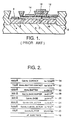
- a representative HBT is illustrated in FIG. 1. It includes a semi-insulating semiconductor substrate 2, typically InP or GaAs.
- a highly doped n+ subcollector layer 4 on the substrate provides an underlying contact with the more lightly n ⁇ doped collector layer 6, with a metallized or highly doped semiconductor pad 8 providing a collector contact through the subcollector.
- a p+ base layer 10 is formed over the collector, with an n doped emitter 12 over the central portion of the base, and a lateral base contact 14 surrounding the emitter.
- An emitter contact 16 is provided on the emitter's upper surface.
- the input voltage forward-biases the base-emitter junction, allowing electrons from the n-type emitter to enter the base.
- the injected electrons travel across the base by diffusion or drift, and are slept into the collector when they reach the base-collector junction by the high fields in this region.
- a homojunction bipolar transistor there is a flow of holes from the base into the emitter across the forward biased base-emitter junction.
- the base doping is made lower than that of the emitter. This, however, makes the base layer more resistive, thereby increasing the device's overall base resistance and degrading its bandwidth.
- a wide-bandgap emitter material is used that creates a higher energy barrier for hole injection into the emitter than the barrier to electron flow into the base, thereby automatically suppressing the base current that is due to hole injection.
- the doping of the base layer can be made as large as possible from solid state chemistry considerations, and the base resistance is correspondingly reduced.
- npn HBTs typically 5-10 ⁇ 1019cm ⁇ 3 beryllium is widely used as the p type base dopant for npn HBTs.
- a significant reliability issue with such devices is that the electric currents and fields generated at the base-emitter junction cause Be to diffuse from the base into the emitter. This movement of Be is characterized by an increase in the emitter-base turn-on voltage as the electrical junction (defined as the location where the dopant concentration of Be equals the n dopant concentration of the emitter) is pushed further into the emitter.
- the Be penetration leads to a reduction in gain, and eventually to complete failure of the transistor.
- This degradation mechanism is currently the operating rate limiting failure mechanism of npn AlInAs/ GaInAs HBTs.
- V eb Eg/q + Kln(Ic)
- V eb the emitter-base turn-on voltage
- Eg the bandgap energy at the electrical junction
- q the electron charge
- K is a constant
- ln the natural logarithm function
- Ic the HBT's collector current.
- the position of the electrical junction is established at the point where the n-dopant concentration in the wide bandgap emitter (typically silicon) equals the p-type Be dopant concentration in the narrow bandgap base.
- the bandgap energy of AlInAs is 1.45ev, while that of GaInAs is 0.75ev. If the electrical junction moves from the more heavily p-doped GaInAs base into the n-doped AlInAs emitter due to Be diffusion, the device's turn-on voltage will increase in proportion to the difference between the bandgap energies of the emitter and base materials, which in this case would be about 700mV. For some applications such as analog-to-digital converters (ADCs), by contrast, it is desirable for the emitter-base turn-on voltage to be controlled to a level of a few mV. For an abrupt emitter-base junction, a movement of the electrical junction by only tens of Angstroms can shift the junction position out of the base and into the emitter, resulting in significant turn-on voltage changes on the order of hundreds of mV.
- ADCs analog-to-digital converters
- the base doping concentration is 1-2 orders of magnitude higher than the emitter doping concentration.
- Be is typically used as the base dopant. It diffuses rapidly, with a concentration-dependent diffusion constant that increases at higher doping levels and can exhibit "explosive" degrees of diffusion when a sufficiently high level of doping (greater than 1019cm ⁇ 3) is attempted. Therefore, the electrical junction is typically determined by Be diffusion into the emitter. This results in a very nonreproducible junction position from wafer to wafer, and even at different locations on a single wafer, since the Be diffusion from the heavily doped base is very sensitive to wafer temperature during growth. In addition, if different base dopings are required, the different Be doping levels will diffuse to different degrees, and this in turn will result in different positionings of the electrical junction.
- One approach to solving the Be diffusion problem uses an undoped layer of low bandgap material, such as GaInAs or GaAs about 100-500 Angstroms thick, between the wide bandgap emitter and the low bandgap base.
- the undoped layer acts as a buffer region into which the base Be can diffuse, so that the bulk of the diffusing Be does not reach the emitter.
- Undoped setback or spacer layers of base material between the base and emitter are also disclosed in Jensen et al., "AlInAs/GaInAs HBT Ic Technology", IEEE Journal of Solid-State Circuits , Vol.26, No.3, March 1991, pages 415-421, and in Nottenburg et al., "In P-Based Heterostructure Bipolar Transistor", Proc. of the 1989 GaAs IC Symnosium , 1989, pages 135-138.
- a short period superlattice is formed between an AlInAs emitter and a GaInAs base.
- the superlattice consists of four sections, with each section having four identical periods; each period had a thickness of 12 Angstroms.
- the ratio of the width of emitter material to the width of base material in each superlattice period varied from about 4:1 in the section adjacent the emitter, to about 1:4 in the section adjacent the base. This structure was proposed as an alternate to a continuously graded interface because of the latter's fabrication difficulties.
- Graded superlattices between p and n doped regions have previously been used in contexts other than HBTs.
- a graded superlattice was employed to eliminate the interface pile-up effect of holes in a "high-low” InP/GaInAs avalanche photodiode in Capasso et al., "Psuedo-quaternary GaInAsP semiconductors: A new Ga 0.47 In 0.53 As/InP graded gap superlattice and its applications to avalanche photodiodes", Applied Physics Letters , Vol.45, No.11, 1 December 1984, pages 1193-1195, and to minimize the effect of carrier trapping at the AlInAs/GaInAs interface of a metal-semiconductor-metal photodiode in Wada et al., "Very high speed GaInAs metal-semiconductor-metal photodiode incorporating an AlInAs/GaInAs graded superl
- the present invention seeks to provide an electrical junction device with a heavily p doped semiconductor material that forms a junction with a more lightly n doped or intrinsic semiconductor material, in which the electrical junction is determined by the device geometry and not by the diffusion of p dopant into the n doped material.
- This goal is accomplished by the provision of a buffer layer between the heavily p doped and the more lightly n doped (or intrinsic) material, with the buffer layer's dopant concentration substantially closer to that of the non-p doped material than to that of the p doped material.
- the doping concentration of the p material is high enough to give at least a portion of the n doped (or intrinsic) material a net p doping through dopant diffusion across a direct contact between the materials.
- the buffer layer is wide enough so that the concentration of diffused dopant from the p doped material does not exceed the doping concentration of the n doped material at the interface between the buffer and the n doped material, thereby establishing the electrical junction at approximately the interface location.
- the invention can be implemented as an HBT, with the p doped and n doped materials respectively forming the device's base and emitter, and the buffer serving in effect as a second base stage.
- the HBT also preferably includes a graded superlattice between the buffer layer and emitter.
- the superlattice has multiple discrete periods, with each period having a layer of the buffer material and a layer of the emitter material; the thicknesses of the base material layers decrease while the thicknesses of the emitter material layers increase in discrete steps for successive periods from the buffer to the emitter.
- a doping is provided to establish the electrical junction within the superlattice, with the superlattice periods on the buffer side of the junction doped p at approximately the buffer dopant concentration, and the superlattice periods on the emitter side of the junction doped n at approximately the emitter dopant concentration. This provides additional resistance to any movement of the electrical junction, and minimizes the effects of any such movement upon the device's emitter-base turn-on voltage.
- the present invention will be described in terms of an HBT with an AlInAs emitter and a GaInAs base. However, it should be understood that it is applicable in general to electrical junction devices in which a p doped region has a significantly higher doping level than an adjacent n doped or intrinsic semiconductor region, and in which the p dopant tends to diffuse into the other region to move the electrical junction between the two, such as the semiconductor lasers, zener diodes and tunneling diodes referred to previously. Also, in the context of an npn HBT, the invention is applicable to other emitter/base combinations, such as AlGaAs/GaAs, GaAs/GaInP and InP/GaInAs.
- the enhanced ability and reliability achieved with the invention make it applicable to any HBT in which a control of the emitter-base turn-on voltage is important, but it is particularly applicable to analog-to-digital converters (ADCs) and digital-to-analog converters (DACs), in which control on the order of millivolts is required.
- ADCs analog-to-digital converters
- DACs digital-to-analog converters
- control on the order of millivolts is required.
- the diffusion of the Be dopant is a kinetically activated process that is greatly accelerated at higher temperatures, enhanced reliability and stability are even more important to achieve in hot environments (100°-200°C) such as those found in automobile engine compartments.
- the present invention divides the base into two sections: the main base with the usual high doping level, and a buffer region between the main base and emitter with a much lower p doping, on the order of the emitter's n doping concentration.
- the base's high doping level offers the high conductivity and low sheet resistance required for fast RF operation of the HBT, while the lightly doped buffer region precisely defines the location of the emitter-base electrical junction.
- FIG. 2 An example of an HBT fabricated in accordance with the invention is shown in FIG. 2.
- the device is preferably formed by MBE on an InP substrate 18, with a 100 Angstrom GaInAs undoped buffer layer 20 over the substrate and then in succession a 7,000 Angstrom GaInAs subcollector layer 22 with an n doping of 1 ⁇ 1019cm ⁇ 3, a 3,000 Angstrom GaInAs collector layer 24 with an n doping concentration of 1 ⁇ 1016cm ⁇ 3, and a 500 Angstrom GaInAs base layer 26 with a p doping concentration of 3 ⁇ 1019cm ⁇ 3.
- a GaInAs base buffer layer 28 is grown on top of the main base layer 26, with a p dopant level that is significantly less than that of the main base.
- the buffer width is selected so that, given the doping level for the main base, the concentration of dopant diffusion from the base falls below the n dopant concentration of an emitter layer 30 at a location within the buffer, or right at the buffer/emitter interface. This ensures that the electrical emitter-base junction occurs at the buffer-emitter interface; this precise location for the electrical junction, independent of dopant diffusion from the base, results in a predictable and repeatable emitter-base turn-on voltage.
- the buffer width is 300 Angstroms, and its p doping level is 2 ⁇ 1018 cm ⁇ 3.
- the emitter 30 that is formed over the buffer has an n dopant concentration of 8 ⁇ 1017 cm ⁇ 3, and is formed from AlInAs 1,200 Angstroms thick.
- a 700 Angstrom AlInAs emitter contact layer 32 with an n doping level of 1 ⁇ 1019cm ⁇ 3 is formed over the emitter 30, followed by a 1,000 Angstrom GaInAs contact layer 34, which has the same n doping level as the emitter contact layer 32.
- Be is a common dopant with MBE grown HBTs, but the invention is also applicable to other p-type base dopants such as carbon. It is also applicable to HBTs formed by metal oxide chemical vapor deposition (MOCVD) with p-type dopants such as Zn, Mn and Mg.
- MOCVD metal oxide chemical vapor deposition
- the buffer layer 28 is conveniently formed from the same material as the base layer 26, this is not essential, so long as these two layers are reasonably lattice matched. Examples of different material combinations that could be used for the base and buffer are GaAs for the base and GaInP for the buffer (with a AlGaAs emitter), or GaInAs for the base and AlInAs for the buffer (with an InP emitter). If desired, the base and buffer materials in the above examples could be switched.
- the base could be doped with Be and the buffer with carbon. While carbon exhibits a lower degree of diffusion than does Be, it is more difficult to activate. However, activating the buffer region is considerably less important than activating the main base.
- the doping level for the buffer layer 28 be substantially less than that of the base 26, on the order of the emitter's doping level. This causes the device's electrical junction to be formed at or very close to the emitter-buffer interface. It is permissible for the buffer doping level to be somewhat higher or lower than that of the emitter, although in that case there may be a small amount of dopant diffusion from the higher into the lower doped layer, with a consequent slight shifting of the electrical junction. In general, the degree of precision in being able to fix the junction location will vary with the closeness of the buffer and emitter doping levels to each other.
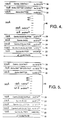
- FIGs. 3a-3c illustrate the electrical junction location for various degrees of base dopant diffusion.
- the base dopant concentration is given by curve 36a, while the buffer dopant concentration is given by step 38 and the emitter dopant concentration by step 40.
- the base dopant concentration follows a generally Gaussian curve; in practice the buffer dopant level would also follow a Gaussian curve, but it is shown as a uniform dopant level for ease of illustration.
- the limits of the buffer region are indicated by dashed lines 38', while an extension of the base dopant profile is indicated by dashed line 36a'.
- the base dopant has undergone little or no diffusion; the electrical junction at which the p dopant level matches the n dopant level is precisely located at the buffer/emitter interface 42.
- the buffer layer could be made considerably thinner.
- FIG. 3b illustrates the optimum situation, in which the buffer layer is just wide enough to establish the electrical junction at the buffer/emitter interface, but no wider.
- the base dopant 36b exhibits a greater diffusion into the buffer layer than in FIG. 3a, and just equals the emitter doping level at the buffer/emitter interface 42.
- the electrical junction is thus still precisely located at this interface, but the buffer layer is no thicker than necessary.
- FIG. 3c illustrates the case in which the base dopant 36c has diffused so far past the buffer layer that its concentration exceeds that of the emitter doping at the buffer/emitter interface.
- the electrical junction is shifted into the emitter to location 44, where the diffused dopant concentration from the base just equals the emitter doping level.
- the width of the buffer layer 38 is thus inadequate, and any slight movement of the diffused base dopant will change the location of the electrical junction, which in turn will alter the emitter-base turn-on voltage.
- a precise positioning of the electrical junction can thus be achieved either by making the doped buffer layer wide enough for a given amount of base dopant diffusion, by restricting the amount of diffusion for a given buffer width, or both.
- a narrow buffer width is preferred because the buffer represents a higher resistivity level than the main base.
- FIGs. 4 and 5 A structure that restricts the base diffusion, and thus allows for a narrow buffer, is shown in FIGs. 4 and 5. It is similar to the HBT of FIG. 2, with common elements identified by the same reference numerals. However, a graded superlattice 46 is inserted between the buffer layer 28 and the emitter 30. As taught in copending application Serial No.
- the superlattice 46 effectively prevents the base dopant from diffusing into the emitter while under operation. Its use together with the buffer layer 28 has been found to be particularly effective in restricting the electrical junction to a desired location.
- the illustrated superlattice consists of multiple successive periods 48, with each period including a layer of buffer material and a layer of emitter material.
- the periods most conveniently have equal thicknesses, but this is not essential. More than five periods are preferred; nine periods are used in the examples of FIGs. 4 and 5.
- the first period has a very thin layer of emitter material and a much thicker layer of buffer material.
- the thicknesses of the two layers are altered in discrete steps for each successive period, with the thickness of the emitter material progressively increasing and that of the buffer material progressively decreasing.
- the layer of buffer material is very thin and the layer of emitter material is much thicker.
- Each period is illustrated as being 33.3 Angstroms thick.
- the first layer of buffer material is 30.0 Angstroms thick, while the first layer of emitter material is 3.3 Angstroms thick.
- the thicknesses of the buffer material layers drop in approximately 3.3 Angstrom steps for each successive period, while the thicknesses of the emitter material layers increase by the same amount.
- the second and third periods from the buffer will have buffer material layers of 26.6 and 23.3 Angstroms and emitter material layers of 6.7 and 10.0 Angstroms, respectively, while the superlattice period nearest the emitter has a 3.3 Angstrom buffer material layer and a 30.0 Angstrom emitter material layer.
- the electrical junction is precisely located within the superlattice by doping the periods on the emitter side of the superlattice n-type at a doping level similar to that of the emitter, and doping the periods on the buffer side of the superlattice p-type at a doping level similar to that of the buffer.
- the n and p doped superlattice periods thus function electrically essentially as extensions of the emitter and buffer, respectively.
- the thickness of the buffer layer 28 has been reduced to 100 Angstroms and the two adjacent superlattice periods are doped p-type and, extend 67 Angstroms into the superlattice, while the remaining periods are doped n-type and have an aggregate thickness of 233 Angstroms.
- the structure of the FIG. 5 example is the same, but the p-doping of the superlattice has been extended to five periods for a depth of 167 Angstroms, with the remaining four periods doped n-type.
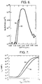
- the base layers of the HBTs shown in FIGs. 4 and 5 were grown by MBE at a low temperature of 300°C with a Be dopant. This low growth temperature has been found to inhibit the diffusion of Be out of the base during its fabrication, as described in copending patent application serial No. by Metzger et al., "Heterojunction Bipolar Transistor Fabrication Method With Low Temperature Base Growth", filed on the same day as the present application and also assigned to Hughes Aircraft Company. Any Be diffusion in the HBTs of FIGs. 4 and 5 could therefore be attributed to the operation of the device, rather than to its fabrication.
- the devices were operated with zero collector-base voltages and one volt collector-emitter voltages.
- Curve 52 closely resembles the doping profile illustrated in FIG. 3a.
- an analysis of the SIMS profile showed that the Be from the heavily doped base of the FIG. 4 sample (curve 50) just diffused to the far edge of the buffer layer (as extended by the p doped portion of the superlattice), in a manner very similar to that illustrated in FIG. 3b.
- the buffer region must extend at least 67 Angstroms into the superlattice to accurately define the location of the electrical junction. If the p-n junction were formed within the superlattice any closer to the base, the electrical junction would instead be defined by dopant diffusion from the heavily doped base.
- the collector currents I c of the HBTs were measured as a function of the emitter-base voltage V eb .
- the results are shown by curves 54 and 56 in FIG. 7 for the devices of FIGs. 4 and 5, respectively.
- the FIG. 5 device exhibited a higher emitter-base turn-on voltage (by approximately 100mV), reflecting a positioning of the electrical junction further into the superlattice from the base.
Landscapes
- Bipolar Transistors (AREA)
Applications Claiming Priority (2)
| Application Number | Priority Date | Filing Date | Title |
|---|---|---|---|
| US08/007,705 US5404028A (en) | 1993-01-22 | 1993-01-22 | Electrical junction device with lightly doped buffer region to precisely locate a p-n junction |
| US7705 | 1998-01-15 |
Publications (1)
| Publication Number | Publication Date |
|---|---|
| EP0607936A1 true EP0607936A1 (de) | 1994-07-27 |
Family
ID=21727700
Family Applications (1)
| Application Number | Title | Priority Date | Filing Date |
|---|---|---|---|
| EP94100700A Withdrawn EP0607936A1 (de) | 1993-01-22 | 1994-01-19 | Elektrisches Übergangsbauelement mit leichtdotiertem Buffergebiet zur präzisen Lokalisierung eines pn-Überganges |
Country Status (3)
| Country | Link |
|---|---|
| US (1) | US5404028A (de) |
| EP (1) | EP0607936A1 (de) |
| JP (1) | JPH077017A (de) |
Cited By (2)
| Publication number | Priority date | Publication date | Assignee | Title |
|---|---|---|---|---|
| WO2000079600A1 (en) * | 1999-06-22 | 2000-12-28 | Hrl Laboratories, Llc | SINGLE HETEROJUNCTION InP-COLLECTOR BJT DEVICE AND METHOD |
| US9530708B1 (en) | 2013-05-31 | 2016-12-27 | Hrl Laboratories, Llc | Flexible electronic circuit and method for manufacturing same |
Families Citing this family (10)
| Publication number | Priority date | Publication date | Assignee | Title |
|---|---|---|---|---|
| TW406337B (en) * | 1997-06-07 | 2000-09-21 | Nat Science Council | Low offset voltage aluminum indium arsen/gallium indium arsen hetreo-junction bipolar transistor (HBT) |
| GB2358959B (en) * | 1999-10-07 | 2002-01-16 | Win Semiconductors Corp | Metamorphic heterojunction bipolar transistor having material structure for low cost fabrication on large size gallium arsenide wafers |
| US6541346B2 (en) | 2001-03-20 | 2003-04-01 | Roger J. Malik | Method and apparatus for a self-aligned heterojunction bipolar transistor using dielectric assisted metal liftoff process |
| US6967144B1 (en) * | 2001-06-20 | 2005-11-22 | National Semiconductor Corporation | Low doped base spacer for reduction of emitter-base capacitance in bipolar transistors with selectively grown epitaxial base |
| US6670654B2 (en) | 2002-01-09 | 2003-12-30 | International Business Machines Corporation | Silicon germanium heterojunction bipolar transistor with carbon incorporation |
| US6822314B2 (en) * | 2002-06-12 | 2004-11-23 | Intersil Americas Inc. | Base for a NPN bipolar transistor |
| TWM253058U (en) * | 2003-09-05 | 2004-12-11 | Visual Photonics Epitaxy Co Lt | Heterogeneous junction dipole transistor structure for adjusting on voltage of base and emitter |
| US7298769B2 (en) * | 2005-05-30 | 2007-11-20 | Mitsubishi Denki Kabushiki Kaisha | Semiconductor laser |
| CN103124876B (zh) | 2010-08-06 | 2016-02-03 | 普司科Ict股份有限公司 | 光学半导体照明设备 |
| JP7685471B2 (ja) | 2022-10-12 | 2025-05-29 | 三菱重工機械システム株式会社 | 搬送装置 |
Citations (1)
| Publication number | Priority date | Publication date | Assignee | Title |
|---|---|---|---|---|
| EP0504925A2 (de) * | 1991-03-21 | 1992-09-23 | Texas Instruments Incorporated | Heteroübergangsbauelement mit einer mehrschichtigen Basis |
Family Cites Families (2)
| Publication number | Priority date | Publication date | Assignee | Title |
|---|---|---|---|---|
| JP2941335B2 (ja) * | 1990-02-20 | 1999-08-25 | 株式会社東芝 | ヘテロ接合バイボーラトランジスタ |
| JPH03280546A (ja) * | 1990-03-29 | 1991-12-11 | Toshiba Corp | ヘテロ接合バイポーラトランジスタ |
-
1993
- 1993-01-22 US US08/007,705 patent/US5404028A/en not_active Expired - Lifetime
-
1994
- 1994-01-19 EP EP94100700A patent/EP0607936A1/de not_active Withdrawn
- 1994-01-24 JP JP6005991A patent/JPH077017A/ja active Pending
Patent Citations (1)
| Publication number | Priority date | Publication date | Assignee | Title |
|---|---|---|---|---|
| EP0504925A2 (de) * | 1991-03-21 | 1992-09-23 | Texas Instruments Incorporated | Heteroübergangsbauelement mit einer mehrschichtigen Basis |
Non-Patent Citations (1)
| Title |
|---|
| K.IKOSSI-ANASTASIOU ET AL., IEEE ELECTRON DEVICE LETTERS, vol. 13, no. 8, August 1992 (1992-08-01), pages 414 - 417, XP000370732 * |
Cited By (3)
| Publication number | Priority date | Publication date | Assignee | Title |
|---|---|---|---|---|
| WO2000079600A1 (en) * | 1999-06-22 | 2000-12-28 | Hrl Laboratories, Llc | SINGLE HETEROJUNCTION InP-COLLECTOR BJT DEVICE AND METHOD |
| US9530708B1 (en) | 2013-05-31 | 2016-12-27 | Hrl Laboratories, Llc | Flexible electronic circuit and method for manufacturing same |
| US10056340B1 (en) | 2013-05-31 | 2018-08-21 | Hrl Laboratories, Llc | Flexible electronic circuit and method for manufacturing same |
Also Published As
| Publication number | Publication date |
|---|---|
| US5404028A (en) | 1995-04-04 |
| JPH077017A (ja) | 1995-01-10 |
Similar Documents
| Publication | Publication Date | Title |
|---|---|---|
| EP0256360B1 (de) | Steuerbare Tunneldiode | |
| US20020121674A1 (en) | Biopolar transistor with lattice matched base layer | |
| EP0313749B1 (de) | Bipolartransistor mit Heteroübergang | |
| US5349201A (en) | NPN heterojunction bipolar transistor including antimonide base formed on semi-insulating indium phosphide substrate | |
| GB1598145A (en) | Semiconductor devices | |
| EP0529772A1 (de) | Verfahren zur Herstellung eines Bipolar-Transistors hoher Zuverlässigkeit mit Heterojunktion | |
| US5404028A (en) | Electrical junction device with lightly doped buffer region to precisely locate a p-n junction | |
| EP0306258B1 (de) | Transistor | |
| US5365077A (en) | Gain-stable NPN heterojunction bipolar transistor | |
| US5561306A (en) | Hetero-bipolar transistor having a plurality of emitters | |
| JPS63140570A (ja) | 半導体装置 | |
| Tokumitsu et al. | InP/InGaAs double heterojunction bipolar transistors grown by metalorganic vapor phase epitaxy with sulfur delta doping in the collector region | |
| US6809400B2 (en) | Composite pinin collector structure for heterojunction bipolar transistors | |
| US5206524A (en) | Heterostructure bipolar transistor | |
| Stellwag et al. | Orientation-dependent perimeter recombination in GaAs diodes | |
| US6049099A (en) | Cadmium sulfide layers for indium phosphide-based heterojunction bipolar transistors | |
| EP0200422A2 (de) | Transistoranordnung | |
| US4772932A (en) | Bipolar transistor and including gas layers between the emitter and base and the base and collector | |
| Lee et al. | In 0.52 Al 0.48 As/In 0.53 Ga 0.47 As/In 0.52 Al 0.48 As abrupt double-heterojunction bipolar transistors | |
| Pan et al. | Reliability of AlGaAs and InGaP heterojunction bipolar transistors | |
| Hill et al. | Uniform, high-gain AlGaAs/In/sub 0.05/Ga/sub 0.95/As/GaAs Pnp heterojunction bipolar transistors by dual selective etch process | |
| EP0361759A2 (de) | Heterostrukturbipolartransistor | |
| EP0358407B1 (de) | Bipolarer Heisselektronen-Transistor | |
| Mohiuddin et al. | Elimination of current blocking in ternary InAlAs-InGaAs-InAlAs double heterojunction bipolar transistors | |
| Goossen et al. | Planarization of emitter-base structure of heterojunction bipolar transistors by doping selective base contact and nonalloyed emitter contact |
Legal Events
| Date | Code | Title | Description |
|---|---|---|---|
| PUAI | Public reference made under article 153(3) epc to a published international application that has entered the european phase |
Free format text: ORIGINAL CODE: 0009012 |
|
| AK | Designated contracting states |
Kind code of ref document: A1 Designated state(s): DE FR GB IT |
|
| 17P | Request for examination filed |
Effective date: 19950118 |
|
| 17Q | First examination report despatched |
Effective date: 19950227 |
|
| STAA | Information on the status of an ep patent application or granted ep patent |
Free format text: STATUS: THE APPLICATION IS DEEMED TO BE WITHDRAWN |
|
| 18D | Application deemed to be withdrawn |
Effective date: 19961015 |