EP0607996A1 - Détecteur linéaire d'images couleurs ayant une distance réduite entre matrices de photocapteurs - Google Patents
Détecteur linéaire d'images couleurs ayant une distance réduite entre matrices de photocapteurs Download PDFInfo
- Publication number
- EP0607996A1 EP0607996A1 EP94100999A EP94100999A EP0607996A1 EP 0607996 A1 EP0607996 A1 EP 0607996A1 EP 94100999 A EP94100999 A EP 94100999A EP 94100999 A EP94100999 A EP 94100999A EP 0607996 A1 EP0607996 A1 EP 0607996A1
- Authority
- EP
- European Patent Office
- Prior art keywords
- transfer gate
- linear image
- gate electrodes
- polysilicon film
- image sensor
- Prior art date
- Legal status (The legal status is an assumption and is not a legal conclusion. Google has not performed a legal analysis and makes no representation as to the accuracy of the status listed.)
- Granted
Links
Images


Classifications
-
- H—ELECTRICITY
- H10—SEMICONDUCTOR DEVICES; ELECTRIC SOLID-STATE DEVICES NOT OTHERWISE PROVIDED FOR
- H10F—INORGANIC SEMICONDUCTOR DEVICES SENSITIVE TO INFRARED RADIATION, LIGHT, ELECTROMAGNETIC RADIATION OF SHORTER WAVELENGTH OR CORPUSCULAR RADIATION
- H10F39/00—Integrated devices, or assemblies of multiple devices, comprising at least one element covered by group H10F30/00, e.g. radiation detectors comprising photodiode arrays
- H10F39/10—Integrated devices
- H10F39/12—Image sensors
- H10F39/15—Charge-coupled device [CCD] image sensors
- H10F39/152—One-dimensional array CCD image sensors
-
- H—ELECTRICITY
- H10—SEMICONDUCTOR DEVICES; ELECTRIC SOLID-STATE DEVICES NOT OTHERWISE PROVIDED FOR
- H10F—INORGANIC SEMICONDUCTOR DEVICES SENSITIVE TO INFRARED RADIATION, LIGHT, ELECTROMAGNETIC RADIATION OF SHORTER WAVELENGTH OR CORPUSCULAR RADIATION
- H10F39/00—Integrated devices, or assemblies of multiple devices, comprising at least one element covered by group H10F30/00, e.g. radiation detectors comprising photodiode arrays
- H10F39/10—Integrated devices
- H10F39/12—Image sensors
- H10F39/15—Charge-coupled device [CCD] image sensors
- H10F39/156—CCD or CID colour image sensors
Definitions
- the present invention relates to a color linear image sensor apparatus, and more specifically to a color linear image sensor apparatus comprising three arrays of photosensor cells.
- the shown conventional color linear image sensor apparatus includes three arrays 1R, 1G and 1B of photoelectric conversion cells, namely, photocells, and a CCD register 2R-1, 2R-2, ⁇ ⁇ ⁇ located at each side of each of these photocell arrays 1A, 1G and 1B.
- these photocell arrays 1R, 1G and 1B have the characteristics having a peak sensitivity in red, in green and in blue, respectively, so that the apparatus functions as a color linear image sensor.
- a distance "L" between each pair of adjacent photocell arrays is ordinarily required to be on the order of 100 ⁇ m to 200 ⁇ m.
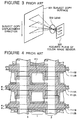
- each of the photocell arrays senses a different position on the same subject copy, as will be apparent from Figure 3 illustrating an optical path diagram in the case of using the color linear image sensor apparatus.
- a color signal processing needs a color signal for red, a color signal for green and a color signal for blue on the same position. Therefore, because of the difference between the positions sensed by the photocell arrays, it was necessary to externally store the color signals of the amount in proportion to the distances "L" between the photocell arrays.
- SRAM static random access memory
- FIG. 2 there is shown an enlarged layout pattern diagram of a portion "A" in Figure 1.
- the CCD register 2R-2 and the CCD register 2G-1 are located between two photocell arrays 1R and 1G, each of which is formed by arranging a number of photodiodes PD (isolated from each other by a channel stopper 6) in a single line.
- Tile CCD register 2R-2 and the CCD register 2G-1 have a first transfer gate electrode 11-1 (formed of a first level polysilicon film) and a second transfer gate electrode 11-2 (formed of a second level polysilicon film), which are common to the CCD register 2R-2 and the CCD register 2G-1.
- the CCD register 2R-2 and the CCD register 2G-1 are isolated from each other by a channel stopper 6A.
- a transfer gate electrode 12-2 (R-2) of the second level polysilicon film
- a transfer gate electrode 12-1 (3G-1) of the second level polysilicon film
- Clock signal wiring conductors 14( ⁇ 1) and 14( ⁇ 2) which also function as a light shield, are connected to the first transfer gate electrode 11-1 and the second transfer gate electrode 11-2 through contact holes C1 and C2, respectively.
- the channel stopper 6A has been required to have a sufficient width to form the contact holes C1 and C2 which connect the clock signal wiring conductors to the first and second gate electrodes, respectively.
- the channel stopper 6A are required to have the width of at least 10 ⁇ m, and preferably about 12 ⁇ m.
- this width of the channel stopper is at least 2 ⁇ m. Therefore, even if the above mentioned design is adopted, the existence of the clock signal wiring conductors is still hindrance in shortening tile distance "L" between the photocell arrays.
- Another object of the present invention is to provide a color linear image sensor apparatus which has a wiring conductor on a channel stopper of a photocell array and which can adopt a two-phase driving method which is the simplest driving method for the CCD register.
- a color linear image sensor apparatus including three linear image sensors which are integrated in parallel to each other on the same semiconductor chip and which have a color sensitivity different from each other, each of the linear image sensors including a photocell array composed of a plurality of photocells arranged in the form of a single array, and a CCD register receiving an electric charge form the photocell array and transferring the received electric charge therethrough, the CCD register being composed of a plurality of alternately located first and second transfer gate electrodes, characterized in that it comprises a wiring conductor formed through an insulating film on a channel stopper which isolates adjacent photocells of each of the linear image sensors from each other, the wiring conductor interconnecting the mutually corresponding first transfer gate electrodes of the three linear image sensors, the wiring conductor being formed of a conducting film of the same level as that of the first transfer gate electrode, and means for connecting each of the second transfer gate electrodes of each of the linear image sensors, to a corresponding first transfer
- first and second transfer gate electrodes are provided for each one of the photocells, the mutually corresponding first transfer gate electrodes of the first and second CCD registers are connected by one wiring conductor formed on each channel stopper region in each photocell array, so that a driving pulse can be applied to the transfer gate electrodes.
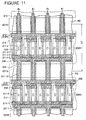
- Figure 5 there is diagrammatically shown an overall structure of a first embodiment of the color linear image sensor apparatus in accordance with the present invention.
- Figure 6 is a partial layout pattern diagram showing a detail of the portion "A" in Figure 5.
- Figure 7 is a sectional view taken along the ling A-A in Figure 6, and
- Figure 8 is a sectional view taken along the ling B-B in Figure 6.
- a linear image sensor for red which is composed of a photocell array 101R and a CCD register 102R-1, 102R-2 located at each side of the photocell array 101R through a transfer gate 103R-1, 103R-2, a linear image sensor for green having a similar arrangement (shown by the same Reference Numerals added with "G” in place of "R"), and a linear image sensor for blue having a similar arrangement (shown by the same Reference Numerals added with "B” in place of "R”).
- mutually corresponding elements between the linear image sensor for red, the linear image sensor for green and the linear image sensor for blue are given the same Reference Numerals suffixed with "R", "G” or "B” for distinction among red, green and blue.
- Reference Symbols VR1, VR2, ⁇ ⁇ ⁇ designate output signals
- Reference Symbols ⁇ 1 and ⁇ 2 indicate two-phase driving pulses for the CCD registers.
- Reference Symbols ⁇ TGR , ⁇ ⁇ ⁇ show pulses for driving the transfer gates 103R-1, ⁇ ⁇ ⁇ .
- One example of ⁇ 1, ⁇ 2 and ⁇ TG (which is a representative of ⁇ TGR , ⁇ TGG and ⁇ TGB ) is shown in the timing chart of Figure 9.
- each of the photocell arrays 101R, ⁇ ⁇ ⁇ is constituted of a number of photodiodes "PD" arranged in a single array.
- each of the photodiodes "PD" includes an N-type region 107-1 formed at a surface portion of a P-type region 105 formed at a principal surface of the N ⁇ silicon substrate 104, and a P+ region 108 formed at a surface of the N-type region 107-1. Adjacent photodiodes are isolated from each other by a P+ channel stopper 106.
- each of the CCD registers 102R-1, ⁇ ⁇ ⁇ comprises a number of first transfer gate electrodes 111-1 (formed of a first level polysilicon film) each formed through a first gate oxide film 110-1 on an N-type region 107-2, and a number of second transfer gate electrodes 111-2 (formed of a second level polysilicon film) each formed through a second gate oxide film 110-2.
- the second level polysilicon film is basically formed above the first level polysilicon film, and each of the second transfer gate electrodes 111-2 partially overrides the first transfer gate electrodes 111-1 positioned at each side of the second transfer gate electrodes 111-2.
- a P ⁇ region 109 is formed at the semiconductor substrate.
- each of the first transfer gate electrodes 111-1 and the second transfer gate electrodes 111-2 is formed to extend over both of the second CCD register (for example, 102R-2) of an upper side linear image sensor and the first CCD register (for example, 102G-1) of a lower side linear image sensor.
- the second CCD register for example, 102R-2
- the first CCD register for example, 102G-1
- the photodiodes of each photocell array are configured to alternately transfer their electric charge to an upper side CCD register and a lower side CCD register through an area that is not blocked by the channel stopper 106.
- Reference Numerals 112-1, 112-2, ⁇ ⁇ ⁇ designate a transfer gate electrode extending along and in parallel the photocell array and passing above the above mentioned areas not blocked by the channel stopper 106, for the purpose of controlling the transfer of the electric charge from the photocell array to the associated CCD register.
- These transfer gate electrodes 112-1, 112-2, ⁇ ⁇ ⁇ are formed of the second level polysilicon film.
- the mutually corresponding first transfer gate electrodes 111-1 of the respective CCD registers are interconnected through a first level polysilicon film 111-1A which is formed through the first gate oxide film 110-1 on the channel stopper of the photocell array.
- Each of the first transfer gate electrodes 111-1 has a portion 111-1B extending to the outside of the CCD registers 102R-1 and 102B-2. As shown in Figure 6, the extending portions 111-1B are alternately connected to wiring conductors 121 for supplying a driving pulse ⁇ 1 and wiring conductors 122 for supplying a driving pulse ⁇ 2.
- each of the first transfer gate electrodes 111-1 is connected through a contact hole "C" to the second transfer gate electrode 111-2 positioned at a right side of the first transfer gate electrode 111-1.
- a light shield is shown by a thick chain line for convenience and given with Reference Numeral 114.
- a width of the channel stopper 106A and a width of the channel stopper in each photocell array are about 2 ⁇ m (under the 2 ⁇ m rule), respectively, and a width of the second level polysilicon film 111-1A is also about 2 ⁇ m (the film 111-1A and the channel stopper 106 just below the film 111-1A are depicted to be different in width for convenience of the drawings, but they actually have substantially the same width).
- the color linear image sensor apparatus having the two-phase driven CCD registers has been constructed.
- the clock signal wiring conductors 14 are connected to the first level polysilicon film and the second level polysilicon film through the contact holes "C1" and "C2".
- the clock signal wiring conductors 14 are ordinarily formed of a metal film such as an aluminum film in order to reduce a wiring resistance.
- the metal permeates into the polysilicon film, and therefore, the polysilicon film in a contact portion and in the neighborhood thereof changes in its film quality. Accordingly, in order to ensure that even if the film quality in the contact hole and in its neighborhood changes, an adverse influence does not exert on the characteristics of the sensor, the P-type channel stopper is provided under the contact holes. In other words, the polysilicon film and the metal have to be contacted to each other on the channel stopper.
- a feature of the second embodiment differing from the first embodiment is that only at one side of each of photocell arrays 201R, ⁇ ⁇ ⁇ , a CCD register 202R, ⁇ ⁇ ⁇ is formed through a transfer gate 203R, ⁇ ⁇ ⁇ (single-channel type).
- first transfer gate electrodes 211-1 and second transfer gates 211-2 are provided for each photocell (photodiode PD) of tile photocell arrays.
- first transfer gate electrodes 211-1 cover through a first gate oxide film (not shown) a coupled portion between the photodiode PD and the CCD register 202R, ⁇ ⁇ ⁇ .
- one 211-11 of the two first transfer gate electrodes for each of one pair of photodiodes is coupled to each other so as to form a C-shaped pattern, and is also coupled to a first level polysilicon film 211-1A1 extending over the channel stopper region 206 in the photocell array 201R, so that a driving clock ⁇ 1 is applied to the first level polysilicon film 211-1A1.
- the other 211-12 of the two first transfer gate electrodes for each of one pair of photodiodes is connected to each other so as to form a C-shaped pattern, and also coupled to a first level polysilicon film 211-A2 extending over a different channel stopper region in the photocell array, so that a driving clock ⁇ 2 is applied to the first level polysilicon film 211-A2.
- the wiring conductors, which are supplied with the driving clocks ⁇ 1 and ⁇ 2 are formed of the first level polysilicon film, and alternately located on the channel stopper regions.
- Each first transfer gate electrode 211-1 is connected through a contact hole "C" to the second transfer gate electrode 211-2 which is paired with the first transfer gate electrode 211-1.
- a single wiring conductor of the first level polysilicon film formed on each channel stopper region can be branched into two wiring conductors within the territory of the CCD register.
- the present invention is characterized in that first transfer gate electrodes of a CCD register associated with each linear image sensor are mutually coupled by a conducting film passing over a channel stopper of a photocell array, and supplied with a corresponding driving clock pulse, and second transfer gate electrodes of the CCD register associated with each linear image sensor are connected to the corresponding first transfer gate electrode through a contact hole formed in a gate oxide film formed under the second transfer gate electrode.
Landscapes
- Solid State Image Pick-Up Elements (AREA)
Applications Claiming Priority (3)
| Application Number | Priority Date | Filing Date | Title |
|---|---|---|---|
| JP872793 | 1993-01-22 | ||
| JP5008727A JPH0785502B2 (ja) | 1993-01-22 | 1993-01-22 | カラーリニアイメージセンサ |
| JP8727/93 | 1993-01-22 |
Publications (2)
| Publication Number | Publication Date |
|---|---|
| EP0607996A1 true EP0607996A1 (fr) | 1994-07-27 |
| EP0607996B1 EP0607996B1 (fr) | 2002-05-15 |
Family
ID=11700987
Family Applications (1)
| Application Number | Title | Priority Date | Filing Date |
|---|---|---|---|
| EP94100999A Expired - Lifetime EP0607996B1 (fr) | 1993-01-22 | 1994-01-24 | Détecteur linéaire d'images couleurs ayant une distance réduite entre matrices de photocapteurs |
Country Status (4)
| Country | Link |
|---|---|
| US (2) | US5631702A (fr) |
| EP (1) | EP0607996B1 (fr) |
| JP (1) | JPH0785502B2 (fr) |
| DE (1) | DE69430600T2 (fr) |
Families Citing this family (13)
| Publication number | Priority date | Publication date | Assignee | Title |
|---|---|---|---|---|
| JP3102348B2 (ja) * | 1996-05-30 | 2000-10-23 | 日本電気株式会社 | カラーリニアイメージセンサおよびその駆動方法 |
| US6169576B1 (en) * | 1996-06-18 | 2001-01-02 | Kabushiki Kaisha Toshiba | Solid state image sensing device having variable resolution and color linear image sensor having variable resolution and control method thereof |
| US5956085A (en) * | 1996-11-07 | 1999-09-21 | Umax Data Systems Inc. | Apparatus for increasing the sample frequency of scanning |
| US6087685A (en) * | 1996-12-12 | 2000-07-11 | Sony Corporation | Solid-state imaging device |
| JP3297988B2 (ja) * | 1997-01-24 | 2002-07-02 | シャープ株式会社 | アクティブマトリクス基板 |
| US6072204A (en) * | 1997-06-23 | 2000-06-06 | Scientific Imaging Technologies, Inc. | Thinned CCD |
| JP3214428B2 (ja) * | 1998-01-05 | 2001-10-02 | 日本電気株式会社 | カラーリニアイメージセンサおよびその駆動方法 |
| US6960161B2 (en) * | 2001-12-28 | 2005-11-01 | Karl Storz Imaging Inc. | Unified electrical and illumination cable for endoscopic video imaging system |
| JP4587642B2 (ja) * | 2003-01-21 | 2010-11-24 | ルネサスエレクトロニクス株式会社 | リニアイメージセンサ |
| JP4454508B2 (ja) * | 2005-01-28 | 2010-04-21 | 三洋電機株式会社 | 固体撮像装置 |
| US8563331B2 (en) * | 2005-06-03 | 2013-10-22 | E. I. Du Pont De Nemours And Company | Process for fabricating and repairing an electronic device |
| TWI618232B (zh) | 2013-09-09 | 2018-03-11 | 應用材料股份有限公司 | 工程誘發的可調靜電效應 |
| JP7159090B2 (ja) * | 2019-03-20 | 2022-10-24 | 株式会社東芝 | 固体撮像装置及び固体撮像装置の制御方法 |
Citations (3)
| Publication number | Priority date | Publication date | Assignee | Title |
|---|---|---|---|---|
| EP0077003A2 (fr) * | 1981-10-09 | 1983-04-20 | Hitachi, Ltd. | Dispositif à l'état solide d'images en couleur |
| EP0435309A1 (fr) * | 1989-12-28 | 1991-07-03 | Kabushiki Kaisha Toshiba | Dispositif capteur d'images en technologie état solide et sa méthode de fabrication |
| EP0495503A2 (fr) * | 1991-01-17 | 1992-07-22 | Sony Corporation | Capteur d'images CCD |
Family Cites Families (7)
| Publication number | Priority date | Publication date | Assignee | Title |
|---|---|---|---|---|
| JPS5941351B2 (ja) * | 1976-09-13 | 1984-10-06 | 株式会社日立製作所 | カラ−用固体撮像素子 |
| JPS5875382A (ja) * | 1981-07-20 | 1983-05-07 | Sony Corp | 固体撮像装置 |
| US4689687A (en) * | 1984-11-13 | 1987-08-25 | Hitachi, Ltd. | Charge transfer type solid-state imaging device |
| JPH0719883B2 (ja) * | 1987-01-26 | 1995-03-06 | 富士写真フイルム株式会社 | 固体撮像装置及びその製造方法 |
| US4847692A (en) * | 1987-01-26 | 1989-07-11 | Fuji Photo Film Co., Ltd. | Solid-state image pickup device with CCDS in an interline transfer system and improved charge transfer electrode structure |
| JPS6434050A (en) * | 1987-07-29 | 1989-02-03 | Canon Kk | Line sensor for reading color |
| US5298777A (en) * | 1991-02-12 | 1994-03-29 | Gold Star Electron Co., Ltd. | CCD image sensor of interlaced scanning type |
-
1993
- 1993-01-22 JP JP5008727A patent/JPH0785502B2/ja not_active Expired - Fee Related
-
1994
- 1994-01-24 DE DE69430600T patent/DE69430600T2/de not_active Expired - Fee Related
- 1994-01-24 EP EP94100999A patent/EP0607996B1/fr not_active Expired - Lifetime
-
1995
- 1995-09-27 US US08/534,307 patent/US5631702A/en not_active Expired - Lifetime
-
1996
- 1996-10-28 US US08/739,041 patent/US5703640A/en not_active Expired - Lifetime
Patent Citations (3)
| Publication number | Priority date | Publication date | Assignee | Title |
|---|---|---|---|---|
| EP0077003A2 (fr) * | 1981-10-09 | 1983-04-20 | Hitachi, Ltd. | Dispositif à l'état solide d'images en couleur |
| EP0435309A1 (fr) * | 1989-12-28 | 1991-07-03 | Kabushiki Kaisha Toshiba | Dispositif capteur d'images en technologie état solide et sa méthode de fabrication |
| EP0495503A2 (fr) * | 1991-01-17 | 1992-07-22 | Sony Corporation | Capteur d'images CCD |
Non-Patent Citations (2)
| Title |
|---|
| H. GOTO: "ADVANCES INLINEAR IMAGE SENSORS", OPTOELECTRONICS DEVICES AND TECHNOLOGIES, vol. 6, no. 2, December 1991 (1991-12-01), TOKYO, JAPAN, pages 333 - 343, XP000264523 * |
| K. MIWADA ET AL.: "6-LINE-SPACE 5KBIT COLOR LINEAR IMAGE SENSOR", ITEJ TECHNICAL REPORT, vol. 15, no. 16, February 1991 (1991-02-01), pages 19 - 24 * |
Also Published As
| Publication number | Publication date |
|---|---|
| US5703640A (en) | 1997-12-30 |
| EP0607996B1 (fr) | 2002-05-15 |
| US5631702A (en) | 1997-05-20 |
| JPH06236982A (ja) | 1994-08-23 |
| JPH0785502B2 (ja) | 1995-09-13 |
| DE69430600D1 (de) | 2002-06-20 |
| DE69430600T2 (de) | 2003-01-16 |
Similar Documents
| Publication | Publication Date | Title |
|---|---|---|
| US5105264A (en) | Color image sensor having an optimum exposure time for each color | |
| US4438455A (en) | Solid-state color imager with three layer four story structure | |
| EP0607996A1 (fr) | Détecteur linéaire d'images couleurs ayant une distance réduite entre matrices de photocapteurs | |
| US6236434B1 (en) | Solid state image pickup device | |
| EP0693786A2 (fr) | Dispositif de prise d'images à l'état solide | |
| US4737833A (en) | Solid-state color image pickup device with accumulated-layer structure | |
| EP0148786B1 (fr) | Méthode de commande d'un capteur d'image à CCD | |
| CN113675228A (zh) | 双行选择结构的布局设计 | |
| US5345319A (en) | Linear color charge coupled device for image sensor and method of driving the same | |
| US4949183A (en) | Image sensor having multiple horizontal shift registers | |
| US4542409A (en) | Single gate line interlace solid-state color imager | |
| KR0186195B1 (ko) | 컬러선형 전하결합소자 및 이의 구동방법 | |
| US4884143A (en) | Lamination type solid image pick up apparatus for avoiding a narrow channel effect | |
| US5262850A (en) | Photoelectric converting device having reduced line sensor space | |
| EP0066767B1 (fr) | Capteur d'images à l'état solide | |
| US4720746A (en) | Frame transfer CCD area image sensor with improved horizontal resolution | |
| US4742239A (en) | Line photosensor with crosstalk suppression | |
| US5485207A (en) | CCD image sensor for normal and mirror images | |
| US4443813A (en) | Solid-state color imager with two layer three story structure | |
| JPH09321938A (ja) | カラーリニアイメージセンサおよびその駆動方法 | |
| JPH07235655A (ja) | 固体撮像装置 | |
| US5369434A (en) | Charge transfer device with high speed transfer rate | |
| JPH06342900A (ja) | 一次元カラーイメージセンサ | |
| US5091922A (en) | Charge transfer device type solid state image sensor having constant saturation level | |
| JPH0211193B2 (fr) |
Legal Events
| Date | Code | Title | Description |
|---|---|---|---|
| PUAI | Public reference made under article 153(3) epc to a published international application that has entered the european phase |
Free format text: ORIGINAL CODE: 0009012 |
|
| 17P | Request for examination filed |
Effective date: 19940421 |
|
| AK | Designated contracting states |
Kind code of ref document: A1 Designated state(s): DE FR GB NL |
|
| 17Q | First examination report despatched |
Effective date: 19970207 |
|
| GRAG | Despatch of communication of intention to grant |
Free format text: ORIGINAL CODE: EPIDOS AGRA |
|
| GRAG | Despatch of communication of intention to grant |
Free format text: ORIGINAL CODE: EPIDOS AGRA |
|
| GRAH | Despatch of communication of intention to grant a patent |
Free format text: ORIGINAL CODE: EPIDOS IGRA |
|
| GRAH | Despatch of communication of intention to grant a patent |
Free format text: ORIGINAL CODE: EPIDOS IGRA |
|
| GRAA | (expected) grant |
Free format text: ORIGINAL CODE: 0009210 |
|
| AK | Designated contracting states |
Kind code of ref document: B1 Designated state(s): DE FR GB NL |
|
| REG | Reference to a national code |
Ref country code: GB Ref legal event code: FG4D |
|
| REF | Corresponds to: |
Ref document number: 69430600 Country of ref document: DE Date of ref document: 20020620 |
|
| ET | Fr: translation filed | ||
| PLBE | No opposition filed within time limit |
Free format text: ORIGINAL CODE: 0009261 |
|
| STAA | Information on the status of an ep patent application or granted ep patent |
Free format text: STATUS: NO OPPOSITION FILED WITHIN TIME LIMIT |
|
| RAP2 | Party data changed (patent owner data changed or rights of a patent transferred) |
Owner name: NEC ELECTRONICS CORPORATION |
|
| 26N | No opposition filed |
Effective date: 20030218 |
|
| NLT2 | Nl: modifications (of names), taken from the european patent patent bulletin |
Owner name: NEC ELECTRONICS CORPORATION |
|
| REG | Reference to a national code |
Ref country code: GB Ref legal event code: 732E |
|
| NLS | Nl: assignments of ep-patents |
Owner name: NEC ELECTRONICS CORPORATION |
|
| REG | Reference to a national code |
Ref country code: FR Ref legal event code: TP |
|
| PGFP | Annual fee paid to national office [announced via postgrant information from national office to epo] |
Ref country code: GB Payment date: 20040121 Year of fee payment: 11 |
|
| PGFP | Annual fee paid to national office [announced via postgrant information from national office to epo] |
Ref country code: FR Payment date: 20040123 Year of fee payment: 11 |
|
| PGFP | Annual fee paid to national office [announced via postgrant information from national office to epo] |
Ref country code: NL Payment date: 20040128 Year of fee payment: 11 |
|
| PGFP | Annual fee paid to national office [announced via postgrant information from national office to epo] |
Ref country code: DE Payment date: 20040325 Year of fee payment: 11 |
|
| PG25 | Lapsed in a contracting state [announced via postgrant information from national office to epo] |
Ref country code: GB Free format text: LAPSE BECAUSE OF NON-PAYMENT OF DUE FEES Effective date: 20050124 |
|
| PG25 | Lapsed in a contracting state [announced via postgrant information from national office to epo] |
Ref country code: NL Free format text: LAPSE BECAUSE OF NON-PAYMENT OF DUE FEES Effective date: 20050801 |
|
| PG25 | Lapsed in a contracting state [announced via postgrant information from national office to epo] |
Ref country code: DE Free format text: LAPSE BECAUSE OF NON-PAYMENT OF DUE FEES Effective date: 20050802 |
|
| GBPC | Gb: european patent ceased through non-payment of renewal fee |
Effective date: 20050124 |
|
| PG25 | Lapsed in a contracting state [announced via postgrant information from national office to epo] |
Ref country code: FR Free format text: LAPSE BECAUSE OF NON-PAYMENT OF DUE FEES Effective date: 20050930 |
|
| NLV4 | Nl: lapsed or anulled due to non-payment of the annual fee |
Effective date: 20050801 |
|
| REG | Reference to a national code |
Ref country code: FR Ref legal event code: ST |