EP0608848B1 - Processeur pour codage cyclique et pour code de vérification de redondance cyclique - Google Patents
Processeur pour codage cyclique et pour code de vérification de redondance cyclique Download PDFInfo
- Publication number
- EP0608848B1 EP0608848B1 EP94101086A EP94101086A EP0608848B1 EP 0608848 B1 EP0608848 B1 EP 0608848B1 EP 94101086 A EP94101086 A EP 94101086A EP 94101086 A EP94101086 A EP 94101086A EP 0608848 B1 EP0608848 B1 EP 0608848B1
- Authority
- EP
- European Patent Office
- Prior art keywords
- data
- bits
- residue
- cyclic
- subjected
- Prior art date
- Legal status (The legal status is an assumption and is not a legal conclusion. Google has not performed a legal analysis and makes no representation as to the accuracy of the status listed.)
- Expired - Lifetime
Links
Images


Classifications
-
- H—ELECTRICITY
- H03—ELECTRONIC CIRCUITRY
- H03M—CODING; DECODING; CODE CONVERSION IN GENERAL
- H03M13/00—Coding, decoding or code conversion, for error detection or error correction; Coding theory basic assumptions; Coding bounds; Error probability evaluation methods; Channel models; Simulation or testing of codes
- H03M13/03—Error detection or forward error correction by redundancy in data representation, i.e. code words containing more digits than the source words
- H03M13/05—Error detection or forward error correction by redundancy in data representation, i.e. code words containing more digits than the source words using block codes, i.e. a predetermined number of check bits joined to a predetermined number of information bits
- H03M13/09—Error detection only, e.g. using cyclic redundancy check [CRC] codes or single parity bit
- H03M13/091—Parallel or block-wise CRC computation
Definitions
- the present invention relates to a processor for cyclic coding and cyclic redundancy code check (hereinafter referred to as "CRC"), and particularly relates to a cyclic coding and CRC processor for error detection and correction of the data received in digital communications.
- CRC cyclic redundancy code check
- Error detection and error correction are techniques at the receiver to accurately receive the data from the transmitter in digital signal communications. Cyclic coding is a process to generate check bits at the transmitter to facilitate such error detection or error correction at the receiver. It may be used for both error detection and error correction corresponding to the type of generator polynomial and available devices at the receiver.
- CRC is a process at the receiver to detect errors in the cyclic coded data as described above.
- the type of the computer, the degree of the generator polynomial and the number of data subjected to be cyclic coding are defined.
- the computer is an 8 bit microcomputer
- the number of data subjected to cyclic coding is 50 bits.
- the 50 bit data for cyclic coding are a 49 , a 48 , .... a 1 and a 0 from the most significant bit (MSB).
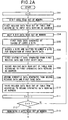
- a cyclic coding and CRC processor in a first conventional Example is effective only when the generator polynomial has a low degree and a small number of data are processed.
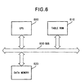
- Fig. 6 it comprises a central processing unit (CPU) 600 for operation, data processing and control with a unit of 8 bits, a data memory 620 which stores 50 bits of the data for cyclic coding in order and a table ROM 610 which stores a syndrome table, all of which are connected with a bus 630.
- CPU central processing unit
- data memory 620 which stores 50 bits of the data for cyclic coding in order
- a table ROM 610 which stores a syndrome table, all of which are connected with a bus 630.
- the table ROM 610 stores a syndrome table prepared in advance.
- the syndrome table substantially has a size of 3 bits ⁇ 50 (50 bytes for a memory of 8 bit units).
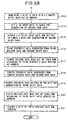
- Step 707 nothing is performed for it.
- Steps 715 to 721 the remaining two bits are also subjected to the same bit judgment.
- the lower 3 bits finally remained in the above parity register in Steps 722 to 724 are used as the parity bits.
- the number of execution states for the first conventional example is calculated to be a value from 1855 states at least to 2851 states at most, depending on whether the data is 1 or 0.
- cyclic coding can be made substantially for any number of data, provided that the degree of the generator polynomial is not more than twice the number of bits in the applicable general-purpose register.
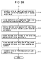
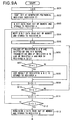
- a processor according to the present invention comprises a CPU 800 and a data memory 820, which are connected with a bus 830 each other, similarly to the first example.
- the CPU 800 sets the number of loops E to be 5 first (Step 901). Next, it sets the generator polynomial registers (two of the general-purpose registers) in the CPU 800 to have 60H (Step 902). Then, in Step 903, the CPU 800 reads out 8 bit data (a 49 to a 42, with a 49 being the MSB) from the data memory 820 and stores the data to register A (one of the general-purpose registers) inside.
- Step 905 the values of registers A and B are shifted by one bit and the MSB of register B is transmitted to the least significant bit (LSB) of register A and the MSB of register A to the carry register (CY).
- the CPU 800 performs the procedure of Steps 904 to 910 for the number of loops (for 48 bits). Then, in Steps 913 to 919, it performs similar bit judgment for the remaining 2 bits.
- the higher 3 bits of the value at register A upon completion of processing are the parity bits (Step 920).
- the number of execution states for the second conventional example is calculated to be a value from 1727 at least to 2095 at most, depending on whether the data is 1 or 0.
- the conventional cyclic coding and CRC processor as described above involves complicated and lengthy processing including judgment process and XOR operation for each bit of data. This limits the time available for other processing such as communication protocol control, and naturally results in an increased cost when a high speed computer is used to reduce time for such processing.
- a cyclic coding processor for a generator polynomial G(X) with a degree of m (m is an integer satisfying m ⁇ n/2) using a computer for data processing by units of n bits comprises residue table storage means which stores a residue table containing 2 n pieces of residue data having n/2 bits obtained by divisions of 2 n pieces of data having n bits by the generator polynomial, data read means which reads out the data having predetermined number of bits for cyclic coding by units of n bits, address generation means which generates addresses of the residue data to be read out from the residue table storage means, residue data read means which reads the residue data out of the residue table storage means according to the generated address, data save means which saves the data subjected to the cyclic coding, data shift means which shifts the data subjected to the cyclic coding and data synthesis means to synthesize the shifted and saved data and the residue data read out.
- the data save means generates save data by saving the lower n/2 bits of the data subjected to cyclic coding
- the data shift means generates the shift data by shifting the higher n/2 bits of the data subjected to the cyclic coding toward the lower n/2 bits
- the data synthesis means generates synthetic data by synthesizing the residue data and the shift data or the residue data and the save data.
- the address generation means uses, for the first address generation, n bit data subjected to cyclic coding read out by the data read means in order to generate the address for the residue table, and for the following address generations, the data obtained by synthesis of the residue data having n/2 bits previously read out and n/2 bits among the n bits subjected to the cyclic coding in order to generate the address for the residue table.
- the address generation means uses, for the first and following address generation processes, the data obtained by synthesis with treating the residue data of n/2 bits previously read out as the higher bits and n/2 bits of the n bits subjected to the cyclic coding as the lower bits in order to generate the address for the residue table.
- a cyclic redundancy check processor for a generator polynomial G(X) with a degree of m (m is an integer satisfying m ⁇ n/2) using a computer for data processing by units of n bits comprises residue table storage means which stores a residue table containing 2 n pieces of residue data having n/2 bits obtained by division of 2 n pieces of data having n bits by the generator polynomial, data read means which reads out the data having predetermined number of bits for cyclic redundancy check by units of n bits, address generation means which generates addresses of the residue data to be read out from the residue table storage means, residue data read means which reads the residue data out of the residue table storage means according to the generated address, data save means which saves the data subjected to the cyclic redundancy check, data shift means which shifts the data subjected to the cyclic redundancy check, data synthesis means to synthesize the shifted and saved data and the residue data read out and check means for parity check of
- the data save means generates save data by saving the lower n/2 bits of the data subjected to cyclic redundancy check
- the data shift means generates the shift data by shifting the higher n/2 bits of the data subjected to the cyclic redundancy check toward the lower n/2 bits
- the data synthesis means generates synthetic data by synthesizing the residue data and the shift data or the residue data and the save data.
- the address generation means uses, for the first address generation, n bit data subjected to cyclic redundancy check read out by the data read means in order to generate the address for the residue table, and for the following address generations, the data obtained by synthesis of the residue data having n/2 bits previously read out and n/2 bits among the n bits subjected to the cyclic redundancy check in order to generate the address for the residue table.
- the address generation means uses, for the first and following address generation processes, the data obtained by synthesis with treating the residue data of n/2 bits previously read out as the higher bits and n/2 bits of the n bits subjected to the cyclic redundancy check as the lower bits in order to generate the address for the residue table.
- Fig. 3 shows the entire configuration of a cyclic coding and CRC processor according to the present invention.
- the reference numeral 100 indicates a CPU for operation, data processing and control by a unit of 8 bits.
- the numeral 200 indicates a table ROM to store a residue table and 300 indicates a data memory to store the data to be changed into cyclic codes.
- the CPU 100, the table ROM 200 and the data memory 300 are connected by a bus 400.
- Fig. 1 is a block diagram to illustrate the function of the CPU 100.
- the CPU 100 comprises a data reader 101 to read out the data to be processed from the data memory 300, a reference address generator 102 to generate addresses for the residue data to be read out of the residue table TR in the table ROM 200, a residue table reader 103 to read out the residue data from the residue table TR in the table ROM 200, a save data generator 104 to save the data read out in the cyclic coding and CRC processing, a shift data generator 105 to shift the data read out in the cyclic coding and CRC processing, a synthetic data generator 106 for data synthesis in the cyclic coding and CRC processing, a repetition controller 107 to control repetition of the cyclic coding and CRC processing and registers 110 to be used for data operation in the cyclic coding and CRC processing.
- the data to be transformed into cyclic codes has 50 bits, which are, from the MSB, ⁇ a 49 , a 48 , ..., a 1 and a 0 ⁇ . These bits are stored in the data memory 300 in this order.
- the table ROM 200 has a residue table TR prepared in advance.
- the residue table TR of the present embodiment to execute cyclic coding for every 8 bits of data has the configuration as described below.
- a data polynomial D(X) is obtained by applying the formula (1) to the above data ⁇ Dk ⁇ except bit d 0 .
- This polynomial D(X) is subjected to division with modulo 2 by the generator polynomial G (X).
- bit d 0 of the data ⁇ Dk ⁇ is added so as to form a 4 bit data ⁇ d 0 , r 0 , r 1 , r 2 ⁇ .
- the residue table TR has 256 pieces of data ⁇ d 0 , r 0 , r 1 , r 2 ⁇ generated for each bit in the data ⁇ Dk ⁇ . Accordingly, the residue table TR in this case has a size of 4 bits ⁇ 256: 256 bytes for an 8 bit unit memory.
- the table ROM 200 of this embodiment which is an 8 bit unit memory, stores the residue table TR and residues are assigned to the higher 4 bits of the 8 bit data.
- the description above can be applied to computers for n-bit processing in general.
- a generator polynomial G(X) of degree m (m is an integer satisfying m ⁇ n/2) is used in cyclic coding and cyclic redundancy code check for predetermined number of data, or in other words, data bits in the data memory 300 are read out by units of n bits for the above processing.
- the residue table can be defined as follows.
- the residue table has 2 n pieces of residue data ⁇ r 0 , ...., r m-1 ⁇ each having a length of n/2 bits, which are generated by modulo 2 division of the data polynomial Da(X) (2) by the generator polynomial G(X).
- the residue table has 2 n pieces of data ⁇ d 0 , ..., d n/2-m+1 , r 0 , ..., r m-1 ⁇ each having a length of n/2 bits obtained by adding the remaining data ⁇ d 0 , ..., d n/2-m+1 ⁇ of the data Dk to the m bit residue data ⁇ r 0 , ..., r m-1 ⁇ as a result of modulo 2 division of the above data polynomial Da(X) by the generator polynomial G (X).
- the generator polynomial G(X) has a degree of "3" and n is 8, and it corresponds to the case where n/2 -m > 0.
- the reference address generator 102 of the CPU 100 uses the above input data to generate an address for the residue table.
- the residue table reader 103 reads out the first residue data (assigned to the higher 4 bits of the 8 bit data) corresponding to the reference address from the residue table TR and stores the data to register A (Step 203).
- the save data generator 104 saves the lower 4 bits of the input data to register B as the first save data (Step 205). Further, the shift data generator 105 of the CPU 100 shifts the higher 4 bits in register E to the lower 4 bits so as to form the first shift data (Step 206).
- the synthetic data generator 106 of the CPU 100 synthesizes the first residue data of register A and the first shift data of register E by OR operation to generate the first synthetic data to be stored in register E (Step 207).
- the reference address generator 102 uses the first synthetic data as the reference address for the residue table TR.
- the residue table reader 103 reads out the second residue data from the residue table TR according to the reference address and stores the data to register A (Step 208).
- the synthetic data generator 106 of the CPU 100 stores the second residue data of register A to register E and stores the first save data to register A. It further ORs the second residue data and the first save data to form the second synthetic data to be stored in register E (Step 209).
- the reference address generator 102 uses the second synthetic data as the reference address for the residue table TR.
- the residue table reader 103 reads out the third residue data from the residue table TR according to the reference address and stores the data to register A (Step 210).
- the CPU 100 continues the above procedure by units of 4 bits for the number of loops (or until the number of loops C becomes "0"). By repeating the procedure of Steps 204 to 210 until the number of loops C becomes "0", 48 bits among 50 bits are processed.
- Step 212 the CPU 100 has its data reader 101 read out the remaining 2 bits of the data among 50 bits from the data memory 300 and store them to register E (Step 213).
- register E the higher two bits are provided with the bits read out of the above data memory 300. In other words, an input data having valid bits at the higher 2 bits among 8 bits is stored.
- the shift data generator 105 shifts the higher 4 bits of the input data to the lower 4 bits so as to generate the second shift data (Step 214).
- the lower two bits of the second shift data is provided with "0".
- the higher 2 bits are provided with the 2 bit data read out of the above data memory 300 and the lower 2 bits are provided with "O".
- the synthetic data generator 106 of the CPU 100 synthesizes the third residue data of register A and the second shift data of register E by OR operation to generate the third synthetic data to be stored in register E (Step 215).
- the reference address generator 102 uses the third synthetic data as a reference address for the residue address TR. According to such reference address, the residue table reader 103 reads out the fourth residue data from the residue table TR to be stored in register A (Step 216).
- the shift data generator 105 of the CPU 100 shifts the fourth residue data by two bits toward lower bit direction and thereby obtains the third shift data (Step 217).
- the higher 2 bits and the lower 2 bits of the third shift data have "0".
- the reference address generator 102 uses the third shift data as the reference address for the residue table TR and the residue table reader 103, according to such reference address, reads out the fifth residue data from the residue table TR (Step 218).
- the higher 3 bits of the fifth residue data are the desired parity bits (Step 219).
- the number of execution states determined from the coding example of Table 3 is found to be 651 states.
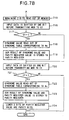
- Fig. 4 shows the configuration of a CRC processor according to a second embodiment of the present invention.
- This processor has a CPU 100a with the same configuration as the CPU 100 of Fig. 1 except addition of a parity checker 120 to check the parity to judge whether the data has any error or not.
- CRC processing is described below.
- the cyclic coding and CRC processing basically follow the same procedure.
- the data transmitter transmits the data in cyclic codes (information bits + parity bits) and the receiver performs CRC processing (error detection with parity check).
- CRC processing error detection with parity check
- 53 bits of data to be subjected to the CRC processing are supposed to be stored in the data memory 300 in appropriate order. These 53 bits comprise 50 bits of cyclic coded data and three parity bits.
- a residue table TR similar to the one described for the first embodiment is prepared in advance and stored in the table ROM 200.
- Steps 501 to 510 the same procedure as the one in Steps 201 to 210 of Fig. 2 is performed and explanation therefor is omitted.
- the data of 53 bits has 50 information bits and three parity bits. Therefore, upon completion of processing in Step 512 (upon completion of data processing for 48 bit data), there remains 5 bits of data. Specifically, the remaining two information bits and three parity bits.
- Step 513 is the number of loops C is "0" in Step 512, the data reader 101 of the CPU 100 reads out the remaining five bits in 53 bit data from the data memory 300 and stores them to register E as input data (Step 513).
- the eight bits are provided with bit numbers from the higher bits in descending order so that the MSB has the bit number 7 and the LSB has the bit number 0 among the eight bits. In other words, among the eight bits of the input data, the higher five bits are provided with the data read out of the data memory 300 (the higher five bits are valid).
- the save data generator 104 saves the third bit in the input data (Bit 3) and treats it as the second save data (Step 514). In this second save data, the third bit in the eight bits (Bit 3) is valid.
- the shift data generator 105 of the CPU 100 shifts the higher four bits of the input data to the lower four bits and treats it as the second shift data (Step 515).
- the synthetic data generator 106 of the CPU 100 synthesizes the third residue data and the second shift data by means of logical OR operation to generate the third synthetic data (Step 516).
- the reference address generator 102 generates third synthetic data as the reference address of the residue table TR and the residue table reader 103 reads out the fourth residue data from the residue table TR according to the reference address (Step 517).
- the synthetic data generator 106 of the CPU 100 synthesizes the fourth residue data and the second save data by means of logical OR operation to generate the fourth synthetic data (Step 518).
- the shift data generator 105 shifts the fourth synthetic data by two bits to the lower bit direction so as to generate the third shift data (Step 519). At this time the higher two bits of the third shift data are set to "0".
- the reference address generator 102 of the CPU 100 generates the third shift data as the reference address of the residue table TR and the residue table reader 103 reads out the fifth residue data from the residue table TR according to the reference address (Step 520). Then, the parity checker 120 checks the higher three bits of the read out fifth residue data (Step 521). If the higher three bits of the fifth residue data are all "0", the system judges that the 53 bit data has no error, and judges that there is an error when even one of the higher three bits is "0".
- the cyclic coding and CRC processing device enables shifting and data synthesis for every n/2 bits because it stores a residue table of 2 n pieces in advance. This reduces the time required for cyclic coding and CRC processing, so that the computer can be effectively utilized for other processing including communication protocol control. Reduction of the time required for cyclic coding and CRC processing also eliminates the need of high speed computers, which reduces the cost of the system.
Landscapes
- Engineering & Computer Science (AREA)
- Computing Systems (AREA)
- Physics & Mathematics (AREA)
- Probability & Statistics with Applications (AREA)
- Theoretical Computer Science (AREA)
- Detection And Correction Of Errors (AREA)
- Error Detection And Correction (AREA)
- Detection And Prevention Of Errors In Transmission (AREA)
Claims (10)
- Processeur de codage cyclique pour un polynôme générateur G(X) avec un degré de m (m étant un nombre entier satisfaisant à la condition m ≤ n/2), au moyen d'un ordinateur pour un traitement de données par unités de n bits, comprenant :caractérisé en ce que lesdits moyens de sauvegarde de données (104) produisent des données de sauvegarde en sauvegardant les n/2 bits inférieurs des données soumises au codage cyclique ;des moyens de mémorisation de table de restes (200), servant à mémoriser une table de restes contenant 2n tronçons de données de restes ayant n/2 bits, obtenus par des divisions de 2n tronçons de données, ayant n bits, par ledit polynôme générateur ;des moyens de lecture de données (101) servant à extraire les données, ayant un nombre prédéterminé de bits, pour un codage cyclique par unités de n bits ;des moyens générateurs d'adresses (102), prévus pour produire des adresses desdites données de restes à extraire desdits moyens de mémorisation de table de restes (200) ;des moyens de lecture de données de restes (103), servant à lire lesdites données de restes à partir desdits moyens de mémorisation de table de restes en fonction de l'adresse produite ;des moyens de sauvegarde de données (104), destinés à sauvegarder les données soumises audit codage cyclique ;des moyens de décalage de données (105) prévus pour décaler les données soumises audit codage cyclique ; etdes moyens de synthèse de données (106) servant à synthétiser lesdites données décalées et sauvegardées et lesdites données de restes extraites ;
lesdits moyens de décalage de données (105) produisent les données à décalage en décalant les n/2 bits supérieurs des données soumises audit codage cyclique vers les n/2 bits inférieurs ; et en ce que
lesdits moyens de synthèse de données (106) produisent des données synthétiques en synthétisant lesdites données de restes et lesdites données à décalage ou lesdites données de restes et lesdites données de sauvegarde. - Processeur de codage cyclique selon la revendication 1, dans lequel lesdits moyens générateurs d'adresses (102) utilisent, pour la production de la première adresse, des données de n bits soumises au codage cyclique et extraites par lesdits moyens de lecture de données (101), afin de produire l'adresse pour ladite table de restes et, pour les générations des adresses suivantes, les données obtenues par la synthèse des données de restes ayant n/2 bits, précédemment extraites, et n/2 bits parmi les n bits soumis audit codage cyclique, pour produire l'adresse pour ladite table de restes.
- Processeur de codage cyclique selon la revendication 2, dans lequel lesdits moyens générateurs d'adresses (102) utilisent, pour les opérations de production de la première adresse et des adresses suivantes, les données obtenues par synthèse en traitant les données de restes de n/2 bits, précédemment extraites, en tant que bits supérieurs, et n/2 bits des n bits soumis au codage cyclique en tant que bits inférieurs afin de produire l'adresse pour ladite table de restes.
- Processeur de codage cyclique selon la revendication 1, dans lequel ladite table de restes comporte 2n tronçons de données de restes, ayant chacun une longueur de n/2 bits obtenue par des divisions modulo 2, par ledit polynôme générateur G(X), des polynômes de donnéespour 2n tronçons de données ayant des groupes de n bits {Dk} (Dk = (d0, ..., di, ..., dn-1) où di est 0 ou 1, i est un nombre entier satisfaisant à la condition 0 ≤ i ≤ n - 1 et k est un nombre entier satisfaisant à la condition 0 ≤ k < 2n.

- Processeur de codage cyclique selon la revendication 4, dans lequel ladite table de restes a, si n/2 - m = 0, 2n tronçons de données de restes {r0, ..., rm-1} ayant chacun une longueur de n/2 bits, obtenus par des divisions modulo 2, par ledit polynôme générateur G(X), des polynômes de donnéespour lesdites données {Dk} et,

si n/2 - m > 0, des données de n/2 bits comprenant 2n tronçons de données de restes de m bits {r0, ..., rm-1} obtenus par des divisions modulo 2, par ledit polynôme générateur G(X), desdits polynômes de données et des données restantes de n/2 - m bits desdites données {Dk}, qui sont {d0, ..., dn/2-m+1}. - Processeur de contrôle de redondance cyclique pour un polynôme générateur G(X) avec un degré de m (m étant un nombre entier satisfaisant à la condition m ≤ n/2), au moyen d'un ordinateur pour un traitement de données par unités de n bits, comprenant :caractérisé en ce que lesdits moyens de sauvegarde de données (104) produisent des données de sauvegarde en sauvegardant les n/2 bits inférieurs des données soumises au contrôle de redondance cyclique ;des moyens de mémorisation de table de restes (200), servant à mémoriser une table de restes contenant 2n tronçons de données de restes ayant n/2 bits, obtenus par des divisions de 2n tronçons de données, ayant n bits, par ledit polynôme générateur ;des moyens de lecture de données (101) servant à extraire les données, ayant un nombre prédéterminé de bits, pour un contrôle de redondance cyclique par unités de n bits ;des moyens générateurs d'adresses, prévus pour produire des adresses desdites données de restes à extraire desdits moyens de mémorisation de table de restes ;des moyens de lecture de données de restes (103), servant à lire lesdites données de restes à partir desdits moyens de mémorisation de table de restes (200) en fonction de l'adresse produite ;des moyens de sauvegarde de données (104), destinés à sauvegarder les données soumises audit contrôle de redondance cyclique ;des moyens de décalage de données (105) prévus pour décaler les données soumises audit contrôle de redondance cyclique ;des moyens de synthèse de données (106) servant à synthétiser lesdites données décalées et sauvegardées et lesdites données de restes extraites ;des moyens de vérification (120) prévus pour un contrôle de parité des données soumises audit contrôle de redondance cyclique, en utilisant les données de restes extraites finalement ;
lesdits moyens de décalage de données (105) produisent les données à décalage en décalant les n/2 bits supérieurs des données soumises audit contrôle de redondance cyclique vers les n/2 bits inférieurs ; et en ce que
lesdits moyens de synthèse de données (106) produisent des données synthétiques en synthétisant lesdites données de restes et lesdites données à décalage ou lesdites données de restes et lesdites données de sauvegarde. - Processeur de contrôle de redondance cyclique selon la revendication 6, dans lequel lesdits moyens générateurs d'adresses (102) utilisent, pour la production de la première adresse, des données de n bits soumises au contrôle de redondance cyclique et extraites par lesdits moyens de lecture de données (101), afin de produire l'adresse pour ladite table de restes et, pour les générations des adresses suivantes, les données obtenues par la synthèse des données de restes ayant n/2 bits, précédemment extraites, et n/2 bits parmi les n bits soumis audit contrôle de redondance cyclique, pour produire l'adresse pour ladite table de restes.
- Processeur de contrôle de redondance cyclique selon la revendication 7, dans lequel lesdits moyens générateurs d'adresses (102) utilisent, pour les opérations de production de la première adresse et des adresses suivantes, les données obtenues par synthèse en traitant les données de restes de n/2 bits, précédemment extraites, en tant que bits supérieurs, et n/2 bits des n bits soumis audit contrôle de redondance cyclique en tant que bits inférieurs afin de produire l'adresse pour ladite table de restes.
- Processeur de contrôle de redondance cyclique selon la revendication 6, dans lequel ladite table de restes comporte 2n tronçons de données de restes, ayant chacun une longueur de n/2 bits, obtenus par des divisions modulo 2, par ledit polynôme générateur G(X), des polynômes de donnéespour 2n tronçons de données ayant des groupes de n bits {Dk} (Dk = (d0, ..., di, ..., dn-1) où di est 0 ou 1, i est un nombre entier satisfaisant à la condition 0 ≤ i ≤ n - 1 et k est un nombre entier satisfaisant à la condition 0 ≤ k ≤ 2n.

- Processeur de contrôle de redondance cyclique selon la revendication 9, dans lequel ladite table de restes a, si n/2 - m = 0, 2n tronçons de données de restes {r0, ..., rm-1} ayant chacun une longueur de n/2 bits, obtenus par des divisions modulo 2, par ledit polynôme générateur G(X), des polynômes de donnéespour lesdites données {Dk} et,

si n/2 - m > 0, des données de n/2 bits comprenant 2n tronçons de données de restes de m bits {r0, ..., rm-1} obtenus par des divisions modulo 2, par ledit polynôme générateur G(X), desdits polynômes de données et des données restantes de n/2 - m bits desdites données {Dk}, qui sont {d0, ..., dn/2-m+1}.
Applications Claiming Priority (3)
| Application Number | Priority Date | Filing Date | Title |
|---|---|---|---|
| JP9636/93 | 1993-01-25 | ||
| JP963693 | 1993-01-25 | ||
| JP5009636A JP3000811B2 (ja) | 1993-01-25 | 1993-01-25 | 巡回符号化およびcrc装置とその処理方法 |
Publications (3)
| Publication Number | Publication Date |
|---|---|
| EP0608848A2 EP0608848A2 (fr) | 1994-08-03 |
| EP0608848A3 EP0608848A3 (fr) | 1997-10-15 |
| EP0608848B1 true EP0608848B1 (fr) | 2002-07-24 |
Family
ID=11725724
Family Applications (1)
| Application Number | Title | Priority Date | Filing Date |
|---|---|---|---|
| EP94101086A Expired - Lifetime EP0608848B1 (fr) | 1993-01-25 | 1994-01-25 | Processeur pour codage cyclique et pour code de vérification de redondance cyclique |
Country Status (4)
| Country | Link |
|---|---|
| US (1) | US5517512A (fr) |
| EP (1) | EP0608848B1 (fr) |
| JP (1) | JP3000811B2 (fr) |
| DE (1) | DE69431008D1 (fr) |
Families Citing this family (12)
| Publication number | Priority date | Publication date | Assignee | Title |
|---|---|---|---|---|
| US5942002A (en) * | 1996-03-08 | 1999-08-24 | Neo-Lore | Method and apparatus for generating a transform |
| US6006354A (en) * | 1997-02-12 | 1999-12-21 | Stmicroelectronics, Inc. | Security device for a video digital to analog converter |
| GB2322526A (en) * | 1997-02-22 | 1998-08-26 | The Technology Partnership Plc | Encoding and decoding data |
| GB9803117D0 (en) * | 1998-02-13 | 1998-04-08 | Sgs Thomson Microelectronics | Cyclic redundancy check in a computer system |
| US6304991B1 (en) * | 1998-12-04 | 2001-10-16 | Qualcomm Incorporated | Turbo code interleaver using linear congruential sequence |
| KR100480286B1 (ko) * | 1999-04-02 | 2005-04-06 | 삼성전자주식회사 | 터보 인터리빙 어드레스 발생 장치 및 방법 |
| US6766490B1 (en) * | 2000-03-03 | 2004-07-20 | Palmone, Inc. | Reduced table size forward error correcting encoder |
| JP4756778B2 (ja) * | 2001-06-14 | 2011-08-24 | サンヨー・オートメディア・センディリアン・バハド | ラジオ・データ・システムの同期方法 |
| GB2377346B (en) * | 2001-07-02 | 2003-10-08 | Matsushita Comm Ind Uk Ltd | Error trapping and correction for cyclic codewords |
| TWI224735B (en) * | 2002-10-25 | 2004-12-01 | Via Tech Inc | Method for storing and accessing data in random bit range between different platforms |
| EP1427109A3 (fr) * | 2002-12-04 | 2004-07-14 | STMicroelectronics Asia Pacific Pte Ltd | Appareil et méthode de calcul de la valeur de redondance cyclique pour un mot de données d'entrée à bits multiples |
| US20060077750A1 (en) * | 2004-10-07 | 2006-04-13 | Dell Products L.P. | System and method for error detection in a redundant memory system |
Family Cites Families (8)
| Publication number | Priority date | Publication date | Assignee | Title |
|---|---|---|---|---|
| JPS63502948A (ja) * | 1986-03-28 | 1988-10-27 | アムペツクス コーポレーシヨン | ワードフレーミング誤差を含む誤差の検出機能を有するデジタルデータ伝送 |
| US4949342A (en) * | 1987-04-14 | 1990-08-14 | Matsushita Electric Industrial Co., Ltd. | Code error detecting method |
| US4964129A (en) * | 1988-12-21 | 1990-10-16 | Bull Hn Information Systems Inc. | Memory controller with error logging |
| US5099484A (en) * | 1989-06-09 | 1992-03-24 | Digital Equipment Corporation | Multiple bit error detection and correction system employing a modified Reed-Solomon code incorporating address parity and catastrophic failure detection |
| EP0431416A3 (en) * | 1989-12-04 | 1992-04-29 | National Semiconductor Corporation | Apparatus and method for accessing a cyclic redundancy error check code generated in parallel |
| CA2050123C (fr) * | 1990-10-11 | 1997-12-09 | Subrahmanyam Dravida | Dispositif et methode de generation parallele de codes de verification aredondance cyclique |
| JPH04365156A (ja) * | 1991-06-13 | 1992-12-17 | Toshiba Corp | データ伝送エラー検出回路 |
| US5359468A (en) * | 1991-08-06 | 1994-10-25 | R-Byte, Inc. | Digital data storage tape formatter |
-
1993
- 1993-01-25 JP JP5009636A patent/JP3000811B2/ja not_active Expired - Lifetime
-
1994
- 1994-01-25 EP EP94101086A patent/EP0608848B1/fr not_active Expired - Lifetime
- 1994-01-25 DE DE69431008T patent/DE69431008D1/de not_active Expired - Lifetime
- 1994-01-25 US US08/186,154 patent/US5517512A/en not_active Expired - Fee Related
Also Published As
| Publication number | Publication date |
|---|---|
| JP3000811B2 (ja) | 2000-01-17 |
| US5517512A (en) | 1996-05-14 |
| EP0608848A2 (fr) | 1994-08-03 |
| EP0608848A3 (fr) | 1997-10-15 |
| DE69431008D1 (de) | 2002-08-29 |
| JPH06224783A (ja) | 1994-08-12 |
Similar Documents
| Publication | Publication Date | Title |
|---|---|---|
| US8127208B2 (en) | Method and apparatus for error management | |
| US4539684A (en) | Automatic frame synchronization recovery utilizing a sequential decoder | |
| JP3234130B2 (ja) | 誤り訂正符号復号化方法およびこの方法を用いる回路 | |
| JP3959788B2 (ja) | 縦及び横のパリティコードを有するデータフレームにおけるエラーを修正するシステム | |
| EP0278383B1 (fr) | Méthode de correction d'erreur utilisant des codes reed-solomon | |
| EP0608848B1 (fr) | Processeur pour codage cyclique et pour code de vérification de redondance cyclique | |
| CN113110954A (zh) | 一种crc码并行计算方法、装置及其应用 | |
| US4570221A (en) | Apparatus for sorting data words on the basis of the values of associated parameters | |
| US4914660A (en) | Method and apparatus for decoding error correcting code | |
| JPS632370B2 (fr) | ||
| US7085988B1 (en) | Hashing system utilizing error correction coding techniques | |
| KR100525987B1 (ko) | 순환 리던던시 코드 서명 비교를 구비한 터보 디코더 | |
| CN101207467B (zh) | 循环冗余校验码的生成和数据序列发送、校验方法及装置 | |
| US5715258A (en) | Error detection code processing device | |
| EP0291961A2 (fr) | Méthode et appareil pour décoder des messages codés en bloc, affectés par des substitutions, des insertions et des suppressions de symboles | |
| US20020124220A1 (en) | Transmission data loss detection system | |
| US6301307B1 (en) | Methods and apparatuses for the transmission and receipt of digital data modulated using quadrature amplitude modulation, and communication devices utilizing such apparatuses and methods | |
| EP0851621B1 (fr) | Modulation codée pour constellations avec un nombre de bits par symbole inférieur à ceux requis par le procédé de codage | |
| JP2621582B2 (ja) | 逐次復号装置 | |
| KR0137354B1 (ko) | 무선 데이타 통신에서의 에러검출 및 정정방법 | |
| JPH08340260A (ja) | 符号誤り訂正回路 | |
| JP2500141B2 (ja) | 誤り訂正方法及び装置 | |
| KR0182007B1 (ko) | 병렬 순회 용장 부호 검사 장치 | |
| JPH0636286B2 (ja) | 誤り訂正方法及び装置 | |
| JP2534563B2 (ja) | 許容誤り逐次訂正回路 |
Legal Events
| Date | Code | Title | Description |
|---|---|---|---|
| PUAI | Public reference made under article 153(3) epc to a published international application that has entered the european phase |
Free format text: ORIGINAL CODE: 0009012 |
|
| AK | Designated contracting states |
Kind code of ref document: A2 Designated state(s): DE FR GB |
|
| PUAL | Search report despatched |
Free format text: ORIGINAL CODE: 0009013 |
|
| AK | Designated contracting states |
Kind code of ref document: A3 Designated state(s): DE FR GB |
|
| 17P | Request for examination filed |
Effective date: 19980122 |
|
| 17Q | First examination report despatched |
Effective date: 19990917 |
|
| GRAG | Despatch of communication of intention to grant |
Free format text: ORIGINAL CODE: EPIDOS AGRA |
|
| GRAG | Despatch of communication of intention to grant |
Free format text: ORIGINAL CODE: EPIDOS AGRA |
|
| GRAH | Despatch of communication of intention to grant a patent |
Free format text: ORIGINAL CODE: EPIDOS IGRA |
|
| GRAH | Despatch of communication of intention to grant a patent |
Free format text: ORIGINAL CODE: EPIDOS IGRA |
|
| GRAA | (expected) grant |
Free format text: ORIGINAL CODE: 0009210 |
|
| AK | Designated contracting states |
Kind code of ref document: B1 Designated state(s): DE FR GB |
|
| REG | Reference to a national code |
Ref country code: GB Ref legal event code: FG4D |
|
| REF | Corresponds to: |
Ref document number: 69431008 Country of ref document: DE Date of ref document: 20020829 |
|
| PG25 | Lapsed in a contracting state [announced via postgrant information from national office to epo] |
Ref country code: DE Free format text: LAPSE BECAUSE OF FAILURE TO SUBMIT A TRANSLATION OF THE DESCRIPTION OR TO PAY THE FEE WITHIN THE PRESCRIBED TIME-LIMIT Effective date: 20021025 |
|
| ET | Fr: translation filed | ||
| PG25 | Lapsed in a contracting state [announced via postgrant information from national office to epo] |
Ref country code: GB Free format text: LAPSE BECAUSE OF NON-PAYMENT OF DUE FEES Effective date: 20030125 |
|
| PLBE | No opposition filed within time limit |
Free format text: ORIGINAL CODE: 0009261 |
|
| STAA | Information on the status of an ep patent application or granted ep patent |
Free format text: STATUS: NO OPPOSITION FILED WITHIN TIME LIMIT |
|
| 26N | No opposition filed |
Effective date: 20030425 |
|
| GBPC | Gb: european patent ceased through non-payment of renewal fee | ||
| PG25 | Lapsed in a contracting state [announced via postgrant information from national office to epo] |
Ref country code: FR Free format text: LAPSE BECAUSE OF NON-PAYMENT OF DUE FEES Effective date: 20030930 |
|
| REG | Reference to a national code |
Ref country code: FR Ref legal event code: ST |