EP0609607A1 - Filtres colorés pour dispositif d'affichage à cristal liquide - Google Patents
Filtres colorés pour dispositif d'affichage à cristal liquide Download PDFInfo
- Publication number
- EP0609607A1 EP0609607A1 EP93307516A EP93307516A EP0609607A1 EP 0609607 A1 EP0609607 A1 EP 0609607A1 EP 93307516 A EP93307516 A EP 93307516A EP 93307516 A EP93307516 A EP 93307516A EP 0609607 A1 EP0609607 A1 EP 0609607A1
- Authority
- EP
- European Patent Office
- Prior art keywords
- film
- colour filter
- intermediate film
- transparent resin
- transparent
- Prior art date
- Legal status (The legal status is an assumption and is not a legal conclusion. Google has not performed a legal analysis and makes no representation as to the accuracy of the status listed.)
- Withdrawn
Links
Images
Classifications
-
- G—PHYSICS
- G02—OPTICS
- G02F—OPTICAL DEVICES OR ARRANGEMENTS FOR THE CONTROL OF LIGHT BY MODIFICATION OF THE OPTICAL PROPERTIES OF THE MEDIA OF THE ELEMENTS INVOLVED THEREIN; NON-LINEAR OPTICS; FREQUENCY-CHANGING OF LIGHT; OPTICAL LOGIC ELEMENTS; OPTICAL ANALOGUE/DIGITAL CONVERTERS
- G02F1/00—Devices or arrangements for the control of the intensity, colour, phase, polarisation or direction of light arriving from an independent light source, e.g. switching, gating or modulating; Non-linear optics
- G02F1/01—Devices or arrangements for the control of the intensity, colour, phase, polarisation or direction of light arriving from an independent light source, e.g. switching, gating or modulating; Non-linear optics for the control of the intensity, phase, polarisation or colour
- G02F1/13—Devices or arrangements for the control of the intensity, colour, phase, polarisation or direction of light arriving from an independent light source, e.g. switching, gating or modulating; Non-linear optics for the control of the intensity, phase, polarisation or colour based on liquid crystals, e.g. single liquid crystal display cells
- G02F1/133—Constructional arrangements; Operation of liquid crystal cells; Circuit arrangements
- G02F1/1333—Constructional arrangements; Manufacturing methods
- G02F1/133345—Insulating layers
-
- G—PHYSICS
- G02—OPTICS
- G02F—OPTICAL DEVICES OR ARRANGEMENTS FOR THE CONTROL OF LIGHT BY MODIFICATION OF THE OPTICAL PROPERTIES OF THE MEDIA OF THE ELEMENTS INVOLVED THEREIN; NON-LINEAR OPTICS; FREQUENCY-CHANGING OF LIGHT; OPTICAL LOGIC ELEMENTS; OPTICAL ANALOGUE/DIGITAL CONVERTERS
- G02F1/00—Devices or arrangements for the control of the intensity, colour, phase, polarisation or direction of light arriving from an independent light source, e.g. switching, gating or modulating; Non-linear optics
- G02F1/01—Devices or arrangements for the control of the intensity, colour, phase, polarisation or direction of light arriving from an independent light source, e.g. switching, gating or modulating; Non-linear optics for the control of the intensity, phase, polarisation or colour
- G02F1/13—Devices or arrangements for the control of the intensity, colour, phase, polarisation or direction of light arriving from an independent light source, e.g. switching, gating or modulating; Non-linear optics for the control of the intensity, phase, polarisation or colour based on liquid crystals, e.g. single liquid crystal display cells
- G02F1/133—Constructional arrangements; Operation of liquid crystal cells; Circuit arrangements
- G02F1/1333—Constructional arrangements; Manufacturing methods
- G02F1/1335—Structural association of cells with optical devices, e.g. polarisers or reflectors
- G02F1/133509—Filters, e.g. light shielding masks
- G02F1/133514—Colour filters
- G02F1/133516—Methods for their manufacture, e.g. printing, electro-deposition or photolithography
-
- G—PHYSICS
- G02—OPTICS
- G02F—OPTICAL DEVICES OR ARRANGEMENTS FOR THE CONTROL OF LIGHT BY MODIFICATION OF THE OPTICAL PROPERTIES OF THE MEDIA OF THE ELEMENTS INVOLVED THEREIN; NON-LINEAR OPTICS; FREQUENCY-CHANGING OF LIGHT; OPTICAL LOGIC ELEMENTS; OPTICAL ANALOGUE/DIGITAL CONVERTERS
- G02F1/00—Devices or arrangements for the control of the intensity, colour, phase, polarisation or direction of light arriving from an independent light source, e.g. switching, gating or modulating; Non-linear optics
- G02F1/01—Devices or arrangements for the control of the intensity, colour, phase, polarisation or direction of light arriving from an independent light source, e.g. switching, gating or modulating; Non-linear optics for the control of the intensity, phase, polarisation or colour
- G02F1/13—Devices or arrangements for the control of the intensity, colour, phase, polarisation or direction of light arriving from an independent light source, e.g. switching, gating or modulating; Non-linear optics for the control of the intensity, phase, polarisation or colour based on liquid crystals, e.g. single liquid crystal display cells
- G02F1/133—Constructional arrangements; Operation of liquid crystal cells; Circuit arrangements
- G02F1/136—Liquid crystal cells structurally associated with a semi-conducting layer or substrate, e.g. cells forming part of an integrated circuit
- G02F1/1362—Active matrix addressed cells
- G02F1/136209—Light shielding layers, e.g. black matrix, incorporated in the active matrix substrate, e.g. structurally associated with the switching element
-
- G—PHYSICS
- G02—OPTICS
- G02F—OPTICAL DEVICES OR ARRANGEMENTS FOR THE CONTROL OF LIGHT BY MODIFICATION OF THE OPTICAL PROPERTIES OF THE MEDIA OF THE ELEMENTS INVOLVED THEREIN; NON-LINEAR OPTICS; FREQUENCY-CHANGING OF LIGHT; OPTICAL LOGIC ELEMENTS; OPTICAL ANALOGUE/DIGITAL CONVERTERS
- G02F1/00—Devices or arrangements for the control of the intensity, colour, phase, polarisation or direction of light arriving from an independent light source, e.g. switching, gating or modulating; Non-linear optics
- G02F1/01—Devices or arrangements for the control of the intensity, colour, phase, polarisation or direction of light arriving from an independent light source, e.g. switching, gating or modulating; Non-linear optics for the control of the intensity, phase, polarisation or colour
- G02F1/13—Devices or arrangements for the control of the intensity, colour, phase, polarisation or direction of light arriving from an independent light source, e.g. switching, gating or modulating; Non-linear optics for the control of the intensity, phase, polarisation or colour based on liquid crystals, e.g. single liquid crystal display cells
- G02F1/133—Constructional arrangements; Operation of liquid crystal cells; Circuit arrangements
- G02F1/1333—Constructional arrangements; Manufacturing methods
- G02F1/1335—Structural association of cells with optical devices, e.g. polarisers or reflectors
- G02F1/133509—Filters, e.g. light shielding masks
- G02F1/133514—Colour filters
- G02F1/133519—Overcoatings
Definitions
- the present invention relates to color filters for a liquid crystal display. More particularly, the present invention relates to color filters having an improved construction whereby a transparent organic resin film and an inorganic conductive film are formed in a manner which prevents foliation and pollution thereof.
- the resultant structure includes an intermediate film provided between the transparent organic resin film and the inorganic conductive film which together planarize and protect the surfaces of color filters.
- LCD liquid crystal displays
- EL electroluminescence
- PDP plasma display panels
- VFD vacuum fluorescence displays
- CRT cathode ray tubes
- LCDs Liquid crystal displays
- LCDs are particularly popular because they are light weight, are thinly manufactured and at a low cost, and have low power consumption. LCDs are widely used in displays for vehicle loading and color television imaging devices, as well as for lap top computers and pocket computers.
- Color LCDs are equally as powerful display mediums as are CRT's.
- Color LCDs are formed by active matrix LCD techniques in which semiconductor fabrication processes are used to form liquid crystal technology.
- thin film transistors constituting switching elements are associated respectively with hundreds and thousands of pixels arranged along a matrix.
- Each TFT operates as a switching element coupled to address wiring for selecting respective pixels and applying a voltage thereto.
- the thin film transistors form a liquid crystal display element and are made using an amorphous silicon or polycrystalline silicon material.
- Amorphous silicon provides stable adhesion onto a broad transparent glass substrate and is therefore preferred.
- An array of thin film transistors formed with amorphous silicon can result in a high picture quality liquid crystal display.
- FIG. 1A shows a sectional view of the structure of conventional color filters for a liquid crystal display.
- a chromium film capable of blocking light is formed over a glass substrate 1' of a liquid crystal display element which has been treated by processes such as cutting and polishing.
- a photoresist layer is subsequently coated over the chromium film and exposed to light. After the deposited chromium film is then etched and patterned to define a plurality of cells, a black matrix 2' is then formed, having a characteristic low ratio of transparency, and patterned in accordance with the etch pattern.
- a material having a select pigment scattered therein to optimize red spectroscopic properties is applied on the transparent glass substrate 1' and on portions of black matrix 2'.
- the result is a colored acrylic photosensitive resin layer formed over select portions of glass substrate 1' and the matrix pattern defined by black matrix 2'.
- This colored resin material is soft-baked for ninety seconds in a hot plate between 80°C to 110°C.
- a transparent resin film such as an anti-oxidation film is applied over the colored resin layer and dried in order to avoid oxidation prior to exposure to light.
- the resultant surface area is then exposed to ultraviolet rays.
- the resin film, impervious to oxygen, is foliated by deionized water for five minutes and the colored photoresist layer is developed using a developer for two or three minutes.
- the colored photoresist layer is rinsed with deionized water for ninety seconds and post-baked in a bake oven at 220°C for thirty minutes to form a first color filter layer (red pattern 3') having optimum red spectroscopic properties.
- a second color filter layer 4' is formed using a colored acrylic photosensitive resin layer having optimum green spectroscopic properties. Second color filter layer 4' is also formed on glass substrate 1' and at a predetermined distance from first color filter layer 3'.
- a third color filter layer 5' having optimum blue spectroscopic properties is formed on glass substrate 1' and at a distance from second color filter layer 4'.
- a transparent resin layer made of acrylic, polyimide, polyacrylate, or polyurethane having high surface solidity and excellent photo-transmittivity is formed to a thickness of 1.5 ⁇ m - 3 ⁇ m. The surface is then soft-baked for an hour in a bake oven at 200°C to form a protective film 6'.
- the upper substrate is completed after formation of a transparent electrode layer 7' formed, for example, from an ITO material, onto which a liquid crystal driving voltage is to be applied.
- Transparent electrode layer 7' is formed over protective film 6' to a thickness of 500 - 1300 angstroms.
- the upper substrate 1' is joined to a lower thin film transistor substrate ("TFT substrate") 10 by adhesive, which is depicted in detail in FIG. 1B.
- TFT substrate thin film transistor substrate
- FIG. 1B illustrates how thin film transistors (TFTs) 12 may be formed as switching elements in a matrix.
- Lower substrate 10 has driving electrodes 14 driving the thin film transistors.
- This lower substrate 10 is joined with upper glass substrate 1' and provided with a liquid crystal layer 16 interposed therebetween.
- the lower substrate 10 and upper glass substrate 1' are joined to each other by applying adhesive 18 to their respective edges.
- This adhesive 18 is applied directly to the protective film 6' or ITO film 7' formed during the steps for forming the color filters 3', 4' and 5'.
- transparent electrode layer 7' is applied to protective film 6' made of an organic transparent resin
- the transparent resin material of protective film 6' is subject to erosion by ion impact which may characteristically result from the excited ITO ion species during the Ar (or ion) sputtering.
- transparent electrode film 7' may combine with transparent resin film 6'.
- transparent electrode film 7' which serves as a signal electrode, will become uneven and polluted with the potential for short circuits (fractures in the ITO film) being formed which would adversely impact image quality.
- protective film 6' made of an organic transparent resin, does not characteristically adhere well to the inorganic transparent electrode film 7', the result is greater likelihood of foliation which can significantly reduce quality and reliability of a color filter region.
- the object of the present invention is to provide color filters for a liquid crystal display which overcome the problem of foliation between an organic transparent resin film and a conductive electrode film, as well as to reduce the likelihood of short circuits and pollution common in conventional devices. This is achieved by forming an intermediate film between the organic transparent resin film and the inorganic transparent conductive electrode film.
- the color filters in the liquid crystal display element formed in accordance with the present invention include: a glass substrate; a matrix defining a plurality of adjacent cells formed on the glass substrate, a pattern of said matrix being such that each cell is spaced a predetermined distance away from corresponding adjacent cells; a plurality of colour filter layers including first, second and third colour filter layers serially arranged and separated respectively by adjacent cells in said matrix; a transparent resin film formed over exposed portions of said matrix and over said plurality of colour filter layers to planarize and protect the surface thereunder; a transparent intermediate film formed on the transparent resin film; and a conductive film formed on the intermediate film.
- the intermediate film is selected so as to provide good adhesion with the transparent resin film and the conductive film, as well as on the basis of such characteristic properties as high photo-transmittivity and solidity so as not to be easily damaged by ion-impact when the conductive film is deposited, by sputtering, on the intermediate film.
- silicon nitride Si3N4 and silicon dioxide SiO2 are good materials for use as the intermediate film, silicon nitride is superior.
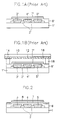
- FIG. 2 depicts a sectional view of color filters formed in a liquid crystal display element in accordance with the present invention.
- the color filters portion of a liquid crystal display of the present invention includes a black matrix 2 defining a plurality of pixels, these pixels are formed at predetermined distances apart and have a predetermined optimal width selected to avoid degradation of thin film transistor regions respectively associated therewith. Pixels are formed of TFT and ITO pixel electrodes.
- first, second and third color filter layers 3, 4, 5, respectively, are serially formed to be separated by adjacent cells in black matrix 2.
- Transparent resin film 6, which serves as a protective film, is then formed over black matrix 2 and color filter layers 3, 4, 5 to planarize and protect the color filter layers.
- An intermediate film 7 is subsequently formed on transparent resin film 6 and a transparent electrode film 8, made from a material such as ITO, is formed on intermediate film 7.
- a metal photoresist film 2 formed for example from chromium, is deposited on a glass substrate 1 by sputtering or by an electron-beam evaporation method.
- the resultant positive photoresist film is coated and soft-baked and then exposed to light for development and formation of a photosensitive pattern.
- the chromium photoresist film is wet-etched in accordance with a selected pattern, then stripped, to form black matrix 2.
- the chromium film should normally be applied to a thickness of 500 to 1500 angstroms.
- a red photoresist film is then coated on selected black matrix 2 to a thickness of 1 to 2 ⁇ m and then soft-baked to achieve wanted spectroscopic properties. Following coating with a transparent resin film of polyvinyl acetate, or polyvinyl alcohol to a thickness of 0.5 to 1 ⁇ m to avoid oxidation, the resultant surface is soft-baked and exposed to light. The resin film for antioxidation is removed and the colored photoresist film is developed and hardened to form a red filter pattern 3.
- green and blue filter layers 4, 5 are formed substantially in the same manner, and a transparent resin film 6, serving as a protective film and made for example from a polyimide, a polyacrylate, or a polyurethane, is coated to a thickness of 1 to 2.5 ⁇ m over black matrix 2 and color filter layers 3, 4, 5, and heated in a bake oven at 200°C for an hour.
- a transparent resin film 6 serving as a protective film and made for example from a polyimide, a polyacrylate, or a polyurethane
- Ammonia and silane gas are then resolved at 130°C to 250°C by a plasma chemical vapor deposition method.
- An intermediate film 7 of for example silicon nitride film is formed to a thickness of 300 to 700 angstroms on transparent resin film 6.
- a transparent electrode film 8 made from indium tin oxide is formed to a thickness of 500 to 2500 angstroms on the transparent resin film 6 by sputtering.
- a photosensitive material is applied to the electrode film 8 and the electrode film 8 is exposed to light and wet-etched. In this manner, a complete set of color filter layers can be appropriately formed.
- a transparent electrode film (normally an inorganic film layer) is formed on a transparent resin film (an organic film layer)
- the organic transparent resin film is eroded by ion impact. This is because when the transparent electrode film is formed on the resin film by sputtering, the resin film is damaged by excited electrode film ions. As a result, the inorganic transparent electrode film is more likely to adhere into the transparent resin film.
- an intermediate film 7 in the present invention made from for example silicon nitride, is formed between the organic transparent resin film 6 and the inorganic transparent electrode film 8 and found to prevent deterioration of LCD image quality that would otherwise result from unevenness or pollution of the overlying transparent electrode film.
- the use of an intermediate film 7 also solves the problem of foliation, common in conventional LCD elements and caused by the poor chemical affinity between adjacent organic and inorganic film layers used in those devices.
- intermediate film 7 is a silicon nitride film layer
- its thickness should not exceed 700 angstroms when the thickness of transparent conductive film 8 (an ITO film) is 500 to 2500 angstroms. This is because the silicon nitride film layer and the ITO film are susceptible to fracture during thermal treatment normally performed following the deposition of the ITO film. This heat treatment subjects the silicon nitride film layer to extreme thermal stress.
- the silicon nitride film is provided with a thickness of less than 300 angstroms, its intended blocking properties are overly degraded. A thickness of less than 300 angstroms is thus not recommended.
- the ideal thickness of a silicon nitride intermediate film layer is in the range of 300 to 700 angstroms; provided that the ITO film is provided with a thickness in the 500 to 2500 angstrom range.
- the optimum thickness of a silicon nitride intermediate film layer will also vary with the type of transparent resin film selected to be coupled therewith.
- Intermediate film 7 should be formed of a material providing good adhesion with both resin film 6 and conductive film 8. This material should provide high photo-transmittivity and solidity so as not to be easily damaged by ion-impact such as may result when conductive film 8 is deposited (by sputtering) thereon.
- silicon dioxide SiO2 can be substituted therefor; although silicon nitride is superior.
- intermediate film 7 is disclosed as being formed between transparent resin film 6 and transparent electrode film 8 so as to overcome the problem of foliation resulting from the poor chemical affinity between an organic resin film and an inorganic conductive film.
- the thickness of intermediate film 7 is disclosed as being important and also optimally selected on the basis of the thickness of the conductive film so as not to adversely influence the spectroscopic properties of the resulting color filter layers in the LCD.
Landscapes
- Physics & Mathematics (AREA)
- Nonlinear Science (AREA)
- Mathematical Physics (AREA)
- Chemical & Material Sciences (AREA)
- Crystallography & Structural Chemistry (AREA)
- General Physics & Mathematics (AREA)
- Optics & Photonics (AREA)
- Engineering & Computer Science (AREA)
- Liquid Crystal (AREA)
- Manufacturing & Machinery (AREA)
- Microelectronics & Electronic Packaging (AREA)
- Optical Filters (AREA)
Applications Claiming Priority (2)
| Application Number | Priority Date | Filing Date | Title |
|---|---|---|---|
| KR1019930001397A KR940020146A (ko) | 1993-02-02 | 1993-02-02 | 액정 디스플레이용 칼라필터 |
| KR931397 | 1993-02-02 |
Publications (1)
| Publication Number | Publication Date |
|---|---|
| EP0609607A1 true EP0609607A1 (fr) | 1994-08-10 |
Family
ID=19350307
Family Applications (1)
| Application Number | Title | Priority Date | Filing Date |
|---|---|---|---|
| EP93307516A Withdrawn EP0609607A1 (fr) | 1993-02-02 | 1993-09-22 | Filtres colorés pour dispositif d'affichage à cristal liquide |
Country Status (3)
| Country | Link |
|---|---|
| EP (1) | EP0609607A1 (fr) |
| JP (1) | JPH06242311A (fr) |
| KR (1) | KR940020146A (fr) |
Cited By (5)
| Publication number | Priority date | Publication date | Assignee | Title |
|---|---|---|---|---|
| EP1835331A1 (fr) * | 2006-03-13 | 2007-09-19 | Samsung Electronics Co., Ltd. | Substrat à filtre couleur et appareil d'affichage le comprenant |
| CN101153933B (zh) * | 2006-09-26 | 2011-08-17 | 奇美电子股份有限公司 | 彩色滤光基板及其制造方法、液晶显示面板与装置 |
| CN101393347B (zh) * | 2007-09-13 | 2014-01-08 | Nlt科技股份有限公司 | 颜色滤光片基板和利用该颜色滤光片基板的lcd装置 |
| WO2015074319A1 (fr) * | 2013-11-21 | 2015-05-28 | 京东方科技集团股份有限公司 | Substrat de film couleur, son procédé de fabrication, panneau tactile "in-cell" et appareil d'affichage |
| CN114424097A (zh) * | 2019-09-13 | 2022-04-29 | 爱色乐居 | 角度滤光器 |
Families Citing this family (4)
| Publication number | Priority date | Publication date | Assignee | Title |
|---|---|---|---|---|
| US6242140B1 (en) | 1997-05-23 | 2001-06-05 | Samsung Sdi Co., Ltd. | Method for manufacturing color filter |
| US7588795B2 (en) | 2000-08-24 | 2009-09-15 | Samsung Mobile Display Co., Ltd. | Manufacturing method of OLED display and apparatus for manufacturing the OLED display |
| JP3827587B2 (ja) * | 2002-02-07 | 2006-09-27 | Nec液晶テクノロジー株式会社 | 反射型又は半透過型液晶表示装置 |
| KR100590929B1 (ko) * | 2003-04-16 | 2006-06-19 | 비오이 하이디스 테크놀로지 주식회사 | 액정표시장치 및 그 제조 방법 |
Citations (5)
| Publication number | Priority date | Publication date | Assignee | Title |
|---|---|---|---|---|
| JPS62144103A (ja) * | 1985-12-18 | 1987-06-27 | Matsushita Electric Ind Co Ltd | カラ−フイルタ− |
| JPS63197903A (ja) * | 1987-02-12 | 1988-08-16 | Nippon Sheet Glass Co Ltd | 透明導電性カラ−フイルタ付基板 |
| US4929060A (en) * | 1987-05-06 | 1990-05-29 | Casio Computer Co., Ltd. | Color liquid crystal display device |
| EP0410387A2 (fr) * | 1989-07-25 | 1991-01-30 | Casio Computer Company Limited | Dispositif d'affichage à cristal liquide et sa méthode de fabrication |
| EP0448139A1 (fr) * | 1990-02-19 | 1991-09-25 | Koninklijke Philips Electronics N.V. | Dispositif à filtre chromatique |
Family Cites Families (1)
| Publication number | Priority date | Publication date | Assignee | Title |
|---|---|---|---|---|
| JPS6199121A (ja) * | 1984-10-22 | 1986-05-17 | Sharp Corp | ツイステツド・ネマテイツク電界効果型液晶表示素子 |
-
1993
- 1993-02-02 KR KR1019930001397A patent/KR940020146A/ko not_active Ceased
- 1993-06-15 JP JP14371093A patent/JPH06242311A/ja active Pending
- 1993-09-22 EP EP93307516A patent/EP0609607A1/fr not_active Withdrawn
Patent Citations (5)
| Publication number | Priority date | Publication date | Assignee | Title |
|---|---|---|---|---|
| JPS62144103A (ja) * | 1985-12-18 | 1987-06-27 | Matsushita Electric Ind Co Ltd | カラ−フイルタ− |
| JPS63197903A (ja) * | 1987-02-12 | 1988-08-16 | Nippon Sheet Glass Co Ltd | 透明導電性カラ−フイルタ付基板 |
| US4929060A (en) * | 1987-05-06 | 1990-05-29 | Casio Computer Co., Ltd. | Color liquid crystal display device |
| EP0410387A2 (fr) * | 1989-07-25 | 1991-01-30 | Casio Computer Company Limited | Dispositif d'affichage à cristal liquide et sa méthode de fabrication |
| EP0448139A1 (fr) * | 1990-02-19 | 1991-09-25 | Koninklijke Philips Electronics N.V. | Dispositif à filtre chromatique |
Non-Patent Citations (2)
| Title |
|---|
| PATENT ABSTRACTS OF JAPAN vol. 11, no. 373 (P - 643) * |
| PATENT ABSTRACTS OF JAPAN vol. 12, no. 483 (P - 802) * |
Cited By (5)
| Publication number | Priority date | Publication date | Assignee | Title |
|---|---|---|---|---|
| EP1835331A1 (fr) * | 2006-03-13 | 2007-09-19 | Samsung Electronics Co., Ltd. | Substrat à filtre couleur et appareil d'affichage le comprenant |
| CN101153933B (zh) * | 2006-09-26 | 2011-08-17 | 奇美电子股份有限公司 | 彩色滤光基板及其制造方法、液晶显示面板与装置 |
| CN101393347B (zh) * | 2007-09-13 | 2014-01-08 | Nlt科技股份有限公司 | 颜色滤光片基板和利用该颜色滤光片基板的lcd装置 |
| WO2015074319A1 (fr) * | 2013-11-21 | 2015-05-28 | 京东方科技集团股份有限公司 | Substrat de film couleur, son procédé de fabrication, panneau tactile "in-cell" et appareil d'affichage |
| CN114424097A (zh) * | 2019-09-13 | 2022-04-29 | 爱色乐居 | 角度滤光器 |
Also Published As
| Publication number | Publication date |
|---|---|
| KR940020146A (ko) | 1994-09-15 |
| JPH06242311A (ja) | 1994-09-02 |
Similar Documents
| Publication | Publication Date | Title |
|---|---|---|
| KR100920321B1 (ko) | 반도체 디바이스 | |
| EP0752121B1 (fr) | Procedes de fabrication d'electrodes de pixels pour affichages a matrice active | |
| US7087180B2 (en) | Method for manufacturing a microlens substrate and method for manufacturing a liquid crystal panel | |
| GB2329061A (en) | Liquid crystal display and method of manufacturing the same. | |
| US8310647B2 (en) | Image display device and manufacturing method of the same | |
| US5400157A (en) | Color filter substrate for a liquid crystal display with terminal portions having same height and same material as those of black matrixes | |
| US5210045A (en) | Dual dielectric field effect transistors for protected gate structures for improved yield and performance in thin film transistor matrix addressed liquid crystal displays | |
| KR100537020B1 (ko) | Ips모드박막트랜지스터용액정표시소자제조방법 | |
| US7145613B2 (en) | Electronic device and method for fabricating the same | |
| EP0609607A1 (fr) | Filtres colorés pour dispositif d'affichage à cristal liquide | |
| JPH0926601A (ja) | 液晶表示装置およびその製造方法 | |
| TW200404185A (en) | Liquid crystal display apparatus and manufacture method of same | |
| US5148248A (en) | Dual dielectric field effect transistors for protected gate structures for improved yield and performance in thin film transistor matrix addressed liquid crystal displays | |
| US20040125254A1 (en) | Liquid crystal display device and method of fabricating the same | |
| US6452210B2 (en) | Thin film transistor substrate and fabricating method thereof | |
| US20040141127A1 (en) | Liquid crystal display | |
| US20040131955A1 (en) | Method of fabricating black matrix | |
| JP2001337348A (ja) | アレイ基板およびその製造方法 | |
| KR101446300B1 (ko) | 전기 영동 표시 장치 및 이의 제조 방법 | |
| JP2838612B2 (ja) | 光弁装置とその製造方法 | |
| US20020151097A1 (en) | Flat panel display and method for forming the same | |
| US5916737A (en) | Method for fabricating liquid crystal display device | |
| KR0182019B1 (ko) | 액정셀 및그 제조 방법 | |
| KR0139348B1 (ko) | 액정표시판넬 제조방법 | |
| US6844901B2 (en) | Liquid crystal display device and method of manufacturing the same |
Legal Events
| Date | Code | Title | Description |
|---|---|---|---|
| PUAI | Public reference made under article 153(3) epc to a published international application that has entered the european phase |
Free format text: ORIGINAL CODE: 0009012 |
|
| AK | Designated contracting states |
Kind code of ref document: A1 Designated state(s): DE FR GB IT |
|
| 17P | Request for examination filed |
Effective date: 19941216 |
|
| STAA | Information on the status of an ep patent application or granted ep patent |
Free format text: STATUS: THE APPLICATION HAS BEEN WITHDRAWN |
|
| 18W | Application withdrawn |
Withdrawal date: 19950203 |