EP0610539B1 - Convertisseur avec un circuit de contrÔle que est alimenté de l'entrée et d'une boucle de rétro-action - Google Patents
Convertisseur avec un circuit de contrÔle que est alimenté de l'entrée et d'une boucle de rétro-action Download PDFInfo
- Publication number
- EP0610539B1 EP0610539B1 EP93102254A EP93102254A EP0610539B1 EP 0610539 B1 EP0610539 B1 EP 0610539B1 EP 93102254 A EP93102254 A EP 93102254A EP 93102254 A EP93102254 A EP 93102254A EP 0610539 B1 EP0610539 B1 EP 0610539B1
- Authority
- EP
- European Patent Office
- Prior art keywords
- output
- voltage
- input
- control circuit
- converter
- Prior art date
- Legal status (The legal status is an assumption and is not a legal conclusion. Google has not performed a legal analysis and makes no representation as to the accuracy of the status listed.)
- Expired - Lifetime
Links
- 230000001105 regulatory effect Effects 0.000 claims abstract description 7
- 238000004804 winding Methods 0.000 claims description 9
- 238000006243 chemical reaction Methods 0.000 abstract 1
- 230000007257 malfunction Effects 0.000 abstract 1
- 239000003990 capacitor Substances 0.000 description 15
- 230000001172 regenerating effect Effects 0.000 description 11
- 230000005669 field effect Effects 0.000 description 7
- 230000000903 blocking effect Effects 0.000 description 6
- 230000005540 biological transmission Effects 0.000 description 4
- 230000006378 damage Effects 0.000 description 2
- 230000002950 deficient Effects 0.000 description 1
- 238000002955 isolation Methods 0.000 description 1
- 230000004048 modification Effects 0.000 description 1
- 238000012986 modification Methods 0.000 description 1
- 238000012544 monitoring process Methods 0.000 description 1
Images

Classifications
-
- H—ELECTRICITY
- H02—GENERATION; CONVERSION OR DISTRIBUTION OF ELECTRIC POWER
- H02M—APPARATUS FOR CONVERSION BETWEEN AC AND AC, BETWEEN AC AND DC, OR BETWEEN DC AND DC, AND FOR USE WITH MAINS OR SIMILAR POWER SUPPLY SYSTEMS; CONVERSION OF DC OR AC INPUT POWER INTO SURGE OUTPUT POWER; CONTROL OR REGULATION THEREOF
- H02M3/00—Conversion of DC power input into DC power output
- H02M3/22—Conversion of DC power input into DC power output with intermediate conversion into AC
- H02M3/24—Conversion of DC power input into DC power output with intermediate conversion into AC by static converters
- H02M3/28—Conversion of DC power input into DC power output with intermediate conversion into AC by static converters using discharge tubes with control electrode or semiconductor devices with control electrode to produce the intermediate AC
- H02M3/325—Conversion of DC power input into DC power output with intermediate conversion into AC by static converters using discharge tubes with control electrode or semiconductor devices with control electrode to produce the intermediate AC using devices of a triode or a transistor type requiring continuous application of a control signal
- H02M3/335—Conversion of DC power input into DC power output with intermediate conversion into AC by static converters using discharge tubes with control electrode or semiconductor devices with control electrode to produce the intermediate AC using devices of a triode or a transistor type requiring continuous application of a control signal using semiconductor devices only
- H02M3/33507—Conversion of DC power input into DC power output with intermediate conversion into AC by static converters using discharge tubes with control electrode or semiconductor devices with control electrode to produce the intermediate AC using devices of a triode or a transistor type requiring continuous application of a control signal using semiconductor devices only with automatic control of the output voltage or current, e.g. flyback converters
Definitions
- the invention relates to a converter as specified in the preamble of claim 1 with a control circuit fed by the input and a feedback circuit.
- Such a converter is already known from DEZ Elektronik 16 / 5.8.1988, pages 44 to 48, in particular page 48, Figure 9 and from DEZ Elektronik 39 (1990) S 134-140.
- the known switching regulator contains a bootstrap circuit, which improves the efficiency when the switching regulator works with a comparatively high input voltage.
- the feed input of the control circuit is connected to the input voltage via a conductive transistor. If the soft start capacitor reaches a predetermined threshold, the transistor is blocked. The operating current of the control circuit is then generated by an additional bootstrap winding of the transformer.
- the regulator circuit arranged on the secondary side influences the duty cycle of switch-on pulses, with the aid of which an electronic switch arranged in the primary-side main circuit in the sense of a constant Output voltage is controlled.
- the control circuit which generates the switch-on pulses, is supplied to improve the efficiency after the start-up phase in normal operation from a regenerative winding of the transformer or, in the case of flow inverters, alternatively from the associated storage choke. If the regulator circuit or the associated transmission path fails, the output voltage and the regenerative voltage can reach impermissibly high values and destroy the connected consumer and / or the own control circuit.
- a monitoring circuit can be provided which monitors the output voltage with the aid of its own reference voltage and detects the excessive output voltage in the event of a fault and switches off the converter via an optocoupler and a primary-side holding circuit. In this way you can protect the consumer or the control circuit from damage or destruction.
- the measures mentioned are associated with a comparatively great effort.
- the object of the invention is to ensure in a converter of the type mentioned that in the event of a failure of the arrangement for regulation or an interruption in the associated transmission path, the output voltage or output voltages and the regenerative voltage are limited with as little effort as possible.
- the converter is designed to achieve the stated object in the manner specified in the characterizing part of patent claim 1.
- the measures according to the invention result in Advantage that the desired limitation of the voltages for applications of the converter, in which there are no particularly narrow limits for possible overvoltages for the output voltage or output voltages, the limitation can be achieved with particularly little additional components.
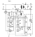
- the capacitor 11 is located at the input and the capacitor 22 at the output.
- the capacitor 11 is supplied with the input voltage U1 from a DC voltage source, not shown in the figure.
- the series circuit consisting of the primary winding 41, the drain-source path of the field effect transistor 13 and the current measuring resistor 12 is connected to the capacitor 11.
- a bipolar transistor can optionally be provided as the switching transistor.
- a variable load resistor can be connected to output b1, b2.
- the output b1, b2 is connected to the secondary winding 42 of the transformer 4 via the rectifier diode 21.
- the secondary circuit of the DC converter contains - starting from the secondary winding 42 - the rectifier diode 21 in a longitudinal branch and the capacitor 22 in a subsequent transverse branch.
- the control circuit 6 is used to control the field effect transistor 13.
- the field effect transistor 13 is connected with its control electrode to the control output e of the control circuit 6.
- the supply voltage input d of the control circuit 6 is connected via the actuator 5 to the terminal a1 of the input.
- the actuator 5 is controlled by the controller 63 contained in the control circuit.
- the actual value input of the controller 63 is connected to the feed input d of the control circuit 6.
- the regenerative winding 43 of the transformer 4 is used to generate a regenerative voltage.
- the series circuit consisting of the rectifier diode 31 and the capacitor 32 is parallel to the regenerative winding 43.
- the output c1, c2 for the regenerative voltage U3 of the flyback converter is connected to the capacitor 32.
- Controller 81 is connected to output b1, b2 of the blocking converter.
- the phototransistor 83 of the optocoupler is at the emitter side at the reference potential.
- the collector of the phototransistor 83 is connected via the resistor 80 to the terminal c1 of the output, which is connected to the reference potential the regenerative voltage U3 connected.
- the voltage divider consisting of resistors 84 and 85 is parallel to the emitter-collector path of phototransistor 83.
- the tap of the voltage divider 84, 85 is connected to the non-inverting input of the comparator 68 contained in the control circuit 6.
- the inverting input of the comparator 68 is located at the junction of the current measuring resistor 12 and the source electrode of the field effect transistor 13.
- the current measuring resistor 12 is connected to reference potential on the input voltage source a1, a
- the control circuit 6 also contains the clock generator 67, to the output of which an arrangement consisting of the logic arrangement 66 and the pulse duration modulator 65 is connected. This arrangement 65, 66 is controlled by the comparator 68. Between the output of the pulse duration modulator 65 and the gate electrode of the field effect transistor 13 is the driver 64, which emits switch-on pulses at its output e with variable duty cycle to the gate electrode of the field effect transistor 13.
- the control circuit 6 also contains the operational amplifier 61 and the reference voltage source 62.
- the output of the operational amplifier 61 is led to the inverting input of the operational amplifier 61 via the series circuit consisting of the capacitor 71 and the resistor 72.
- the non-inverting input of the operational amplifier 61 with an open collector output is connected to the reference voltage source 62.
- the inverting input of the operational amplifier 61 is at the tap of the voltage divider consisting of the resistors 33 and 34 and lying parallel to the capacitor 32.
- an operational amplifier with push-pull output can be used for the collector output.
- a decoupling diode must be inserted between the output of the operational amplifier and the connection point of the resistor 80 with the collector of the optocoupler.
- the output of the operational amplifier 61 is connected directly to the collector of the phototransistor 83.
- the output of the operational amplifier 61 and the output of the optocoupler 82, 83 are therefore directly connected to one another.
- This connection of the outputs has led via resistor 80 to connection c1 for the further output voltage U3 serving as auxiliary voltage.
- This arrangement forms an OR-type circuit.
- the voltage at the voltage divider 84, 85 is determined during normal operation by the output of the optocoupler 83 and in the event of a fault by the output of the operational amplifier 61.
- the voltage at the tap of the divider 84, 85 forms the setpoint for the subordinate current control.
- the regenerative voltage U3 also increases approximately proportionally to the output voltage U2.
- the regenerative voltage U3 is compared via the voltage divider 33, 34 in the integrated operational amplifier 61 of the control circuit with the reference voltage U Ref of the reference voltage transmitter 62, which is also contained in the control module.
- this control circuit replaces the defective voltage control and sets the pulse duty factor of the switch-on pulses by means of an EMF control so that a constant voltage U3 results.
- the output voltage U2 also remains regulated or limited to a value slightly higher than the regulation by the regulator 81.
- the RC element 71, 72 forms a negative feedback circuit, which gives the control loop a stable behavior. In this way, consumers and control circuit of the converter are effectively protected against overvoltages by only four additional passive components 33, 34, 71, 72.
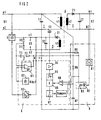
- the blocking converter shown in FIG. 2 differs from that according to FIG. 1 in that the inverting input of the comparator 68 is not connected to the terminal of the current measuring resistor 12 carrying voltage relative to the reference potential, but to another arrangement, the voltage pulses increasing with time Generated amplitude.
- This arrangement contains the series circuit consisting of the resistor 86 and the capacitor 87, connected to the input voltage U1, and the ramp generator 69.
- the inverting input of the comparator 68 is at the connection point of the resistor 86 and the capacitor 87 and thus to the terminal which leads to the reference potential voltage of the capacitor 87 connected.
- At the inverting input of the comparator 68 there is also the output of the ramp generator 69 controlled by the clock generator 67, which periodically discharges the capacitor 87.
- blocking inverters are shown in FIGS. 1 and 2. The same can be done for others Direct current converters, in particular flow converters, limit the output voltage.
- An integrated control module is preferably used as the control circuit.
- the pulse duty factor of the switch-on pulses is changed in each case in that the switch-on pulses of a predetermined repetition frequency are shortened in terms of their duration depending on the response of a comparator.
- An expedient modification of this regulation can consist in that the pulse duty factor is changed by changing the repetition frequency or both the repetition frequency and the pulse duration.
- An oscillator with a voltage-controlled frequency can be used to change the pulse repetition frequency.
- Fig. 3 shows two output characteristics of a flyback converter in comparison.
- the output characteristic curve A applies to a regulated output voltage.
- the output characteristic curve B shows the voltage curve if the output voltage is limited by EMF control. The limitation of the output voltage by the EMF control starts at a somewhat higher voltage value than it results from the control of the output voltage.
Landscapes
- Engineering & Computer Science (AREA)
- Power Engineering (AREA)
- Dc-Dc Converters (AREA)
- Input Circuits Of Receivers And Coupling Of Receivers And Audio Equipment (AREA)
- Transmitters (AREA)
Claims (6)
- Convertisseur statique de fréquence comportant un interrupteur (13) électronique, disposé en série avec un enroulement primaire (41) d'un transformateur (4) et pouvant être commandé par un circuit (6) de commande, au moins un circuit secondaire connecté à un enroulement (42) de sortie du transformateur et destiné à produire une tension de sortie, et un dispositif (8) de régulation de la tension (U2) de sortie par changement du taux d'impulsion des impulsions de branchement fournies par le circuit (6) de commande à l'interrupteur électronique (13), une entrée (d) de tension d'alimentation du circuit de commande étant connectée à la fois à un circuit (43,31,32) d'alimentation en retour du convertisseur statique de fréquence et, par l'intermédiaire d'un organe (5) de réglage, à l'entrée (a1) du convertisseur statique de fréquence, le dispositif (8) de réglage de la tension de sortie comportant un régulateur (81) ainsi qu'un optocoupleur (82,83) branché en aval du régulateur et à sortie à collecteur ouvert et un diviseur (33,34) de tension étant branché en parallèle avec la sortie du circuit (43,31,32) d'alimentation en retour,
caractérisé en ce queil est prévu dans le circuit (6) de commande un amplificateur opérationnel (61) de limitation de la tension en cas d'erreur, un circuit RC (71,72) étant prévu entre la sortie et l'entrée inverseuse de l'amplificateur opérationnel (61),l'entrée inverseuse est reliée à la prise médiane du diviseur (33,34) de tension,la sortie de l'amplificateur opérationnel (61) est reliée à la fois à la voie émetteur-collecteur (83) de l'optocoupleur et à l'entrée non inverseuse d'un comparateur (68) intégré au circuit de commande etl'entrée inverseuse du comparateur (68) est reliée à une voie de tension du côté primaire (41) du transformateur (4). - Convertisseur statique de fréquence suivant la revendication 1,
caractérisé en ce que
l'entrée non inverseuse de l'amplificateur (61) opérationnel est reliée dans le circuit (6) de commande à une source (62) de tension de référence et la sortie de l'amplificateur opérationnel (61) est reliée conjointement avec la sortie de l'optocoupleur (82,83) par l'intermédiaire d'une résistance commune (80) à la tension (U3) d'alimentation en retour. - Convertisseur statique de fréquence suivant l'une des revendications précédentes,
caractérisé en ce que
des impulsions de tension d'amplitude croissante en fonction du temps peuvent être appliquées à une entrée du comparateur (68), dont l'autre entrée est reliée à la sortie du montage (8) de régulation de la tension (U2) de sortie et à l'aide duquel les impulsions de branchement produites par une horloge (67) peuvent être écourtées dans le temps. - Convertisseur statique de fréquence suivant la revendication 3,
caractérisé en ce que
l'une des entrées du comparateur (68) est connectée à une résistance (12) de mesure du courant disposée dans le circuit primaire (1) du convertisseur statique de fréquence. - Convertisseur statique de fréquence suivant la revendication 4,
caractérisé en ce que
l'une des entrées du comparateur (68) est connectée à la sortie d'un générateur de rampes (69). - Convertisseur statique de fréquence suivant l'une des revendications précédentes,
caractérisé en ce que
un diviseur (84,85) de tension est disposé entre la sortie de l'optocoupleur (82,83) et un potentiel de référence et l'autre entrée du comparateur (68) est connectée à la prise du diviseur (84,85) de tension.
Priority Applications (3)
| Application Number | Priority Date | Filing Date | Title |
|---|---|---|---|
| DE59306398T DE59306398D1 (de) | 1993-02-12 | 1993-02-12 | Umrichter mit einer vom Eingang und einem Rückspeisekreis gespeisten Steuerschaltung |
| AT93102254T ATE152867T1 (de) | 1993-02-12 | 1993-02-12 | Umrichter mit einer vom eingang und einem rückspeisekreis gespeisten steuerschaltung |
| EP93102254A EP0610539B1 (fr) | 1993-02-12 | 1993-02-12 | Convertisseur avec un circuit de contrÔle que est alimenté de l'entrée et d'une boucle de rétro-action |
Applications Claiming Priority (1)
| Application Number | Priority Date | Filing Date | Title |
|---|---|---|---|
| EP93102254A EP0610539B1 (fr) | 1993-02-12 | 1993-02-12 | Convertisseur avec un circuit de contrÔle que est alimenté de l'entrée et d'une boucle de rétro-action |
Publications (2)
| Publication Number | Publication Date |
|---|---|
| EP0610539A1 EP0610539A1 (fr) | 1994-08-17 |
| EP0610539B1 true EP0610539B1 (fr) | 1997-05-07 |
Family
ID=8212601
Family Applications (1)
| Application Number | Title | Priority Date | Filing Date |
|---|---|---|---|
| EP93102254A Expired - Lifetime EP0610539B1 (fr) | 1993-02-12 | 1993-02-12 | Convertisseur avec un circuit de contrÔle que est alimenté de l'entrée et d'une boucle de rétro-action |
Country Status (3)
| Country | Link |
|---|---|
| EP (1) | EP0610539B1 (fr) |
| AT (1) | ATE152867T1 (fr) |
| DE (1) | DE59306398D1 (fr) |
Families Citing this family (1)
| Publication number | Priority date | Publication date | Assignee | Title |
|---|---|---|---|---|
| JP3391774B2 (ja) | 2000-10-20 | 2003-03-31 | Smk株式会社 | 間欠動作型スイッチング電源回路 |
-
1993
- 1993-02-12 DE DE59306398T patent/DE59306398D1/de not_active Expired - Fee Related
- 1993-02-12 EP EP93102254A patent/EP0610539B1/fr not_active Expired - Lifetime
- 1993-02-12 AT AT93102254T patent/ATE152867T1/de not_active IP Right Cessation
Also Published As
| Publication number | Publication date |
|---|---|
| ATE152867T1 (de) | 1997-05-15 |
| EP0610539A1 (fr) | 1994-08-17 |
| DE59306398D1 (de) | 1997-06-12 |
Similar Documents
| Publication | Publication Date | Title |
|---|---|---|
| DE69111738T2 (de) | Verlustfreier Dämpfungskreis. | |
| DE19537896B4 (de) | Kontroller für eine Schaltmodus-Leistungsversorgungseinrichtung und Schaltmodus-Leistungsversorgungseinrichtung unter Verwendung des Kontrollers | |
| EP0498917B1 (fr) | Convertisseur commandé par horloge avec limitation de courant | |
| DE10040413B4 (de) | Schaltungsanordnung zur Erzeugung eines Schaltsignals für ein stromgesteuertes Schaltnetzteil | |
| DE19745218C2 (de) | Steuerschaltung und Verfahren zur Steuerung des Schaltens von MOS-Gate-gesteuerten Leistungshalbleiterbauteilen | |
| DE10214190B4 (de) | Stromversorgung mit mehreren parallel geschalteten Schaltnetzteilen | |
| DE2935811A1 (de) | Geschalteter spannungswandler | |
| EP2157834A2 (fr) | Installation de commutation destinée au fonctionnement d'au moins une source lumineuse semi-conductrice | |
| DE60128995T2 (de) | Gate-Treiber für Thyristor | |
| EP2709257A2 (fr) | Circuit de convertisseur de courant et procédé de commande du circuit de convertisseur de courant | |
| EP0380033A2 (fr) | Disposition de circuit pour alimentation à découpage à récuperation à circuit résonnant | |
| DE60101694T2 (de) | Rückkopplungsschleife für Leistungsumwandler | |
| EP0696102A1 (fr) | Convertisseur direct avec une circuit de sortie auxiliaire | |
| EP0099596B1 (fr) | Circuit d'alimentation en courant électrique | |
| DE4421249A1 (de) | Schaltstromversorgungsgerät mit Snubber-Schaltung | |
| EP0590304A2 (fr) | Procédé pour la commande pilote d'une alimentation en courant commutée pour légalisation de la tension d'alimentation | |
| EP0727062A1 (fr) | Alimentation a decoupage | |
| DE102006038474A1 (de) | Stromrichter | |
| EP0024523B1 (fr) | Convertisseur de passage monophasé pour générer des tensions de sortie à courant continu électriquement séparées | |
| DE10339470A1 (de) | Steuerschaltung für ein Schaltnetzteil | |
| DE60013681T2 (de) | Ein Gleichspannungswandler mit mehrere Ausgängen, insbesondere zum Betrieb in Fahrzeugen | |
| EP0610539A1 (fr) | Convertisseur avec un circuit de contrôle que est alimenté de l'entrée et d'une boucle de rétro-action | |
| EP2555402B1 (fr) | Convertisseur | |
| DE3300285C2 (de) | Elektronisches Schaltnetzteil | |
| EP0302433B1 (fr) | Convertisseur à récupération |
Legal Events
| Date | Code | Title | Description |
|---|---|---|---|
| PUAI | Public reference made under article 153(3) epc to a published international application that has entered the european phase |
Free format text: ORIGINAL CODE: 0009012 |
|
| AK | Designated contracting states |
Kind code of ref document: A1 Designated state(s): AT BE CH DE DK ES FR GB IT LI |
|
| 17P | Request for examination filed |
Effective date: 19940915 |
|
| 17Q | First examination report despatched |
Effective date: 19950126 |
|
| GRAG | Despatch of communication of intention to grant |
Free format text: ORIGINAL CODE: EPIDOS AGRA |
|
| GRAH | Despatch of communication of intention to grant a patent |
Free format text: ORIGINAL CODE: EPIDOS IGRA |
|
| GRAH | Despatch of communication of intention to grant a patent |
Free format text: ORIGINAL CODE: EPIDOS IGRA |
|
| GRAH | Despatch of communication of intention to grant a patent |
Free format text: ORIGINAL CODE: EPIDOS IGRA |
|
| GRAA | (expected) grant |
Free format text: ORIGINAL CODE: 0009210 |
|
| AK | Designated contracting states |
Kind code of ref document: B1 Designated state(s): AT BE CH DE DK ES FR GB IT LI |
|
| PG25 | Lapsed in a contracting state [announced via postgrant information from national office to epo] |
Ref country code: IT Free format text: LAPSE BECAUSE OF FAILURE TO SUBMIT A TRANSLATION OF THE DESCRIPTION OR TO PAY THE FEE WITHIN THE PRESCRIBED TIME-LIMIT;WARNING: LAPSES OF ITALIAN PATENTS WITH EFFECTIVE DATE BEFORE 2007 MAY HAVE OCCURRED AT ANY TIME BEFORE 2007. THE CORRECT EFFECTIVE DATE MAY BE DIFFERENT FROM THE ONE RECORDED. Effective date: 19970507 Ref country code: GB Effective date: 19970507 Ref country code: FR Effective date: 19970507 Ref country code: ES Free format text: THE PATENT HAS BEEN ANNULLED BY A DECISION OF A NATIONAL AUTHORITY Effective date: 19970507 Ref country code: DK Effective date: 19970507 |
|
| REF | Corresponds to: |
Ref document number: 152867 Country of ref document: AT Date of ref document: 19970515 Kind code of ref document: T |
|
| REG | Reference to a national code |
Ref country code: CH Ref legal event code: NV Representative=s name: SIEMENS SCHWEIZ AG Ref country code: CH Ref legal event code: EP |
|
| REF | Corresponds to: |
Ref document number: 59306398 Country of ref document: DE Date of ref document: 19970612 |
|
| EN | Fr: translation not filed | ||
| GBV | Gb: ep patent (uk) treated as always having been void in accordance with gb section 77(7)/1977 [no translation filed] |
Effective date: 19970507 |
|
| PGFP | Annual fee paid to national office [announced via postgrant information from national office to epo] |
Ref country code: AT Payment date: 19980210 Year of fee payment: 6 |
|
| PG25 | Lapsed in a contracting state [announced via postgrant information from national office to epo] |
Ref country code: BE Free format text: LAPSE BECAUSE OF NON-PAYMENT OF DUE FEES Effective date: 19980228 |
|
| PLBE | No opposition filed within time limit |
Free format text: ORIGINAL CODE: 0009261 |
|
| STAA | Information on the status of an ep patent application or granted ep patent |
Free format text: STATUS: NO OPPOSITION FILED WITHIN TIME LIMIT |
|
| PGFP | Annual fee paid to national office [announced via postgrant information from national office to epo] |
Ref country code: DE Payment date: 19980420 Year of fee payment: 6 |
|
| 26N | No opposition filed | ||
| PGFP | Annual fee paid to national office [announced via postgrant information from national office to epo] |
Ref country code: CH Payment date: 19980515 Year of fee payment: 6 |
|
| BERE | Be: lapsed |
Owner name: SIEMENS A.G. Effective date: 19980228 |
|
| PG25 | Lapsed in a contracting state [announced via postgrant information from national office to epo] |
Ref country code: AT Free format text: LAPSE BECAUSE OF NON-PAYMENT OF DUE FEES Effective date: 19990212 |
|
| PG25 | Lapsed in a contracting state [announced via postgrant information from national office to epo] |
Ref country code: LI Free format text: LAPSE BECAUSE OF NON-PAYMENT OF DUE FEES Effective date: 19990228 Ref country code: CH Free format text: LAPSE BECAUSE OF NON-PAYMENT OF DUE FEES Effective date: 19990228 |
|
| REG | Reference to a national code |
Ref country code: CH Ref legal event code: PL |
|
| PG25 | Lapsed in a contracting state [announced via postgrant information from national office to epo] |
Ref country code: DE Free format text: LAPSE BECAUSE OF NON-PAYMENT OF DUE FEES Effective date: 19991201 |