EP0610621A2 - Verfahren mit Pull-down und Pull-up elementen und digitale logische Schaltung - Google Patents
Verfahren mit Pull-down und Pull-up elementen und digitale logische Schaltung Download PDFInfo
- Publication number
- EP0610621A2 EP0610621A2 EP93308894A EP93308894A EP0610621A2 EP 0610621 A2 EP0610621 A2 EP 0610621A2 EP 93308894 A EP93308894 A EP 93308894A EP 93308894 A EP93308894 A EP 93308894A EP 0610621 A2 EP0610621 A2 EP 0610621A2
- Authority
- EP
- European Patent Office
- Prior art keywords
- pull
- channel transistor
- coupled
- logic circuit
- digital logic
- Prior art date
- Legal status (The legal status is an assumption and is not a legal conclusion. Google has not performed a legal analysis and makes no representation as to the accuracy of the status listed.)
- Ceased
Links
Images
Classifications
-
- H—ELECTRICITY
- H03—ELECTRONIC CIRCUITRY
- H03K—PULSE TECHNIQUE
- H03K19/00—Logic circuits, i.e. having at least two inputs acting on one output; Inverting circuits
- H03K19/01—Modifications for accelerating switching
- H03K19/017—Modifications for accelerating switching in field-effect transistor circuits
- H03K19/01707—Modifications for accelerating switching in field-effect transistor circuits in asynchronous circuits
- H03K19/01721—Modifications for accelerating switching in field-effect transistor circuits in asynchronous circuits by means of a pull-up or down element
-
- H—ELECTRICITY
- H03—ELECTRONIC CIRCUITRY
- H03K—PULSE TECHNIQUE
- H03K19/00—Logic circuits, i.e. having at least two inputs acting on one output; Inverting circuits
- H03K19/20—Logic circuits, i.e. having at least two inputs acting on one output; Inverting circuits characterised by logic function, e.g. AND, OR, NOR, NOT circuits
Definitions
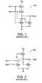
- NOR gate 100 The output line 103 of NOR gate 100 is typically connected to a CMOS buffer (not shown) which functions as a driver for NOR gate 100. Note that an inverter (also not shown) coupled to line 103 transforms NOR gate 100 into an OR gate. Thus, a NOR gate circuit is used to implement both OR or NOR logic functions.
Landscapes
- Physics & Mathematics (AREA)
- Engineering & Computer Science (AREA)
- Computer Hardware Design (AREA)
- Computing Systems (AREA)
- General Engineering & Computer Science (AREA)
- Mathematical Physics (AREA)
- Logic Circuits (AREA)
- Electronic Switches (AREA)
Applications Claiming Priority (2)
| Application Number | Priority Date | Filing Date | Title |
|---|---|---|---|
| US08/017,084 US5408145A (en) | 1993-02-12 | 1993-02-12 | Low power consumption and high speed NOR gate integrated circuit |
| US17084 | 1993-02-12 |
Publications (2)
| Publication Number | Publication Date |
|---|---|
| EP0610621A2 true EP0610621A2 (de) | 1994-08-17 |
| EP0610621A3 EP0610621A3 (en) | 1995-09-27 |
Family
ID=21780643
Family Applications (1)
| Application Number | Title | Priority Date | Filing Date |
|---|---|---|---|
| EP93308894A Ceased EP0610621A3 (en) | 1993-02-12 | 1993-11-08 | Digital logic circuit and method having pull-down and pull-up devices. |
Country Status (5)
| Country | Link |
|---|---|
| US (1) | US5408145A (de) |
| EP (1) | EP0610621A3 (de) |
| JP (1) | JPH06252740A (de) |
| KR (1) | KR940020690A (de) |
| TW (1) | TW245834B (de) |
Cited By (1)
| Publication number | Priority date | Publication date | Assignee | Title |
|---|---|---|---|---|
| DE10239813B4 (de) * | 2002-08-29 | 2005-09-29 | Advanced Micro Devices, Inc., Sunnyvale | Elektronische Schaltung mit verbesserter Stromstabilisierung |
Families Citing this family (7)
| Publication number | Priority date | Publication date | Assignee | Title |
|---|---|---|---|---|
| US5517133A (en) * | 1993-07-14 | 1996-05-14 | Sun Microsystems, Inc. | Multiple-input OR-gate employing a sense amplifier |
| US5945848A (en) * | 1996-11-19 | 1999-08-31 | Rockwell Semiconductor Systems, Inc. | Effectively differential, multiple input OR/NOR gate architecture |
| US6137313A (en) * | 1997-06-20 | 2000-10-24 | Altera Corporation | Resistive pull-up device for I/O pin |
| US6329851B1 (en) * | 2000-04-17 | 2001-12-11 | Lsi Logic Corporation | Power-on reset cell |
| US6259275B1 (en) | 2000-05-01 | 2001-07-10 | Rn2R, L.L.C. | Logic gate having reduced power dissipation and method of operation thereof |
| US7830179B2 (en) | 2007-11-22 | 2010-11-09 | Samsung Electronics Co., Ltd. | Multi-functional logic gate device and programmable integrated circuit device using the same |
| CN104658508B (zh) * | 2015-03-24 | 2017-06-09 | 京东方科技集团股份有限公司 | 一种移位寄存器单元、栅极驱动电路及显示装置 |
Family Cites Families (8)
| Publication number | Priority date | Publication date | Assignee | Title |
|---|---|---|---|---|
| US4797580A (en) * | 1987-10-29 | 1989-01-10 | Northern Telecom Limited | Current-mirror-biased pre-charged logic circuit |
| GB2226727B (en) * | 1988-10-15 | 1993-09-08 | Sony Corp | Address decoder circuits for non-volatile memories |
| EP0380095B1 (de) * | 1989-01-25 | 1995-11-08 | Hitachi, Ltd. | Logische Schaltung |
| US4972102A (en) * | 1989-05-08 | 1990-11-20 | Motorola, Inc. | Single-ended sense amplifier with dual feedback and a latching disable mode that saves power |
| US5117130A (en) * | 1990-06-01 | 1992-05-26 | At&T Bell Laboratories | Integrated circuits which compensate for local conditions |
| US5151622A (en) * | 1990-11-06 | 1992-09-29 | Vitelic Corporation | CMOS logic circuit with output coupled to multiple feedback paths and associated method |
| US5187394A (en) * | 1992-01-13 | 1993-02-16 | Motorola, Inc. | Configurable row decoder driver circuit |
| US5291076A (en) * | 1992-08-31 | 1994-03-01 | Motorola, Inc. | Decoder/comparator and method of operation |
-
1993
- 1993-02-12 US US08/017,084 patent/US5408145A/en not_active Expired - Fee Related
- 1993-08-17 TW TW082106581A patent/TW245834B/zh active
- 1993-11-08 EP EP93308894A patent/EP0610621A3/en not_active Ceased
- 1993-11-30 JP JP5299707A patent/JPH06252740A/ja not_active Withdrawn
- 1993-12-28 KR KR1019930030190A patent/KR940020690A/ko not_active Withdrawn
Cited By (2)
| Publication number | Priority date | Publication date | Assignee | Title |
|---|---|---|---|---|
| DE10239813B4 (de) * | 2002-08-29 | 2005-09-29 | Advanced Micro Devices, Inc., Sunnyvale | Elektronische Schaltung mit verbesserter Stromstabilisierung |
| US7020485B2 (en) | 2002-08-29 | 2006-03-28 | Advanced Micro Devices, Inc. | Electronic circuit with improved current stabilization |
Also Published As
| Publication number | Publication date |
|---|---|
| EP0610621A3 (en) | 1995-09-27 |
| TW245834B (en) | 1995-04-21 |
| JPH06252740A (ja) | 1994-09-09 |
| KR940020690A (ko) | 1994-09-16 |
| US5408145A (en) | 1995-04-18 |
Similar Documents
| Publication | Publication Date | Title |
|---|---|---|
| EP0223786B1 (de) | Ttl/cmos-eingangspuffer | |
| US5894238A (en) | Output buffer with static and transient pull-up and pull-down drivers | |
| KR100591520B1 (ko) | 감소된 전압 입출력의 3상태 버퍼 및 그 제조 방법 | |
| US4347447A (en) | Current limiting MOS transistor driver circuit | |
| US6911860B1 (en) | On/off reference voltage switch for multiple I/O standards | |
| US5097148A (en) | Integrated circuit buffer with improved drive capability | |
| EP0788235B1 (de) | Digitale Spannungspegelumsetzer und Systeme damit | |
| US6069515A (en) | High voltage input buffer circuit using low voltage transistors | |
| JP3759756B2 (ja) | 結合された論理ゲートおよびラッチ | |
| US6225838B1 (en) | Integrated circuit buffers having reduced power consumption requirements | |
| US5408145A (en) | Low power consumption and high speed NOR gate integrated circuit | |
| US6169432B1 (en) | High voltage switch for providing voltages higher than 2.5 volts with transistors made using a 2.5 volt process | |
| EP1537666B1 (de) | Rekonfigurierbare logikanordnung mit schaltungen zur modulation der betriebsspannung von mos transistoren | |
| US20020067189A1 (en) | Domino logic with low-threshold NMOS pull-up | |
| JP3742335B2 (ja) | 入出力バッファ回路 | |
| US5952850A (en) | Input/output circuit and a method for controlling an input/output signal | |
| US6268759B1 (en) | Low-power 5-volt input/output tolerant circuit with power-down control for a low voltage CMOS crossbar switch | |
| US5717355A (en) | Method and apparatus with active feedback for shifting the voltage level of a signal | |
| JP3221459B2 (ja) | 入力回路 | |
| US5898320A (en) | Programmable interconnect point having reduced crowbar current | |
| JP3583442B2 (ja) | 高速振幅制限プルアップ回路 | |
| KR950024211A (ko) | 반도체집적회로의 바이씨모오스 레벨변환회로 및 이를 이용한 데이타출력버퍼 | |
| KR930008658B1 (ko) | 전압레벨 검출회로 | |
| US6559678B1 (en) | Node predisposition circuit | |
| WO2008028012A1 (en) | Junction field effect transistor input buffer level shifting circuit |
Legal Events
| Date | Code | Title | Description |
|---|---|---|---|
| PUAI | Public reference made under article 153(3) epc to a published international application that has entered the european phase |
Free format text: ORIGINAL CODE: 0009012 |
|
| AK | Designated contracting states |
Kind code of ref document: A2 Designated state(s): BE DE DK ES FR GB GR IE IT LU NL PT SE |
|
| PUAL | Search report despatched |
Free format text: ORIGINAL CODE: 0009013 |
|
| AK | Designated contracting states |
Kind code of ref document: A3 Designated state(s): BE DE DK ES FR GB GR IE IT LU NL PT SE |
|
| 17P | Request for examination filed |
Effective date: 19960308 |
|
| 17Q | First examination report despatched |
Effective date: 19961223 |
|
| GRAG | Despatch of communication of intention to grant |
Free format text: ORIGINAL CODE: EPIDOS AGRA |
|
| 18R | Application refused |
Effective date: 19971206 |