EP0613180A2 - Halbleiteranordnung mit Verbindungselektroden - Google Patents
Halbleiteranordnung mit Verbindungselektroden Download PDFInfo
- Publication number
- EP0613180A2 EP0613180A2 EP94108007A EP94108007A EP0613180A2 EP 0613180 A2 EP0613180 A2 EP 0613180A2 EP 94108007 A EP94108007 A EP 94108007A EP 94108007 A EP94108007 A EP 94108007A EP 0613180 A2 EP0613180 A2 EP 0613180A2
- Authority
- EP
- European Patent Office
- Prior art keywords
- layer
- semiconductor element
- insulating film
- contact hole
- wiring
- Prior art date
- Legal status (The legal status is an assumption and is not a legal conclusion. Google has not performed a legal analysis and makes no representation as to the accuracy of the status listed.)
- Ceased
Links
Images


Classifications
-
- H—ELECTRICITY
- H10—SEMICONDUCTOR DEVICES; ELECTRIC SOLID-STATE DEVICES NOT OTHERWISE PROVIDED FOR
- H10W—GENERIC PACKAGES, INTERCONNECTIONS, CONNECTORS OR OTHER CONSTRUCTIONAL DETAILS OF DEVICES COVERED BY CLASS H10
- H10W20/00—Interconnections in chips, wafers or substrates
- H10W20/40—Interconnections external to wafers or substrates, e.g. back-end-of-line [BEOL] metallisations or vias connecting to gate electrodes
- H10W20/41—Interconnections external to wafers or substrates, e.g. back-end-of-line [BEOL] metallisations or vias connecting to gate electrodes characterised by their conductive parts
- H10W20/425—Barrier, adhesion or liner layers
-
- H—ELECTRICITY
- H10—SEMICONDUCTOR DEVICES; ELECTRIC SOLID-STATE DEVICES NOT OTHERWISE PROVIDED FOR
- H10D—INORGANIC ELECTRIC SEMICONDUCTOR DEVICES
- H10D64/00—Electrodes of devices having potential barriers
- H10D64/60—Electrodes characterised by their materials
- H10D64/62—Electrodes ohmically coupled to a semiconductor
Definitions
- the present invention relates to a semiconductor device having wiring electrodes and, more particularly, to a semiconductor device wired through contact holes.
- a MOS transistor has, for example, n-type diffusion regions in the surface area of a p-type silicon substrate. These regions are used as a source and drain.
- Contact holes are formed by patterning an insulating layer covering the substrate and diffusion layers. Wiring layers are formed, extending through the contact holes and contacting the diffusion layers.
- Al is deposited on the diffusion layer by sputtering, and alloyed with Si by annealing.
- the Al diffuses from the wiring layer into the silicon substrate, growing Al-Si spikes within the substrate.
- shallow diffusion layers are often formed with a use of BF2 and BCl2, and, in this case, the alloy spikes may grow deeper than the diffusion layer. If spikes penetrate the diffusion layer and reach the substrate, the pn junction between the substrate and the diffusion layer will break down.
- the contact resistance of the wiring layer undesirably increases due to the low conductivity.
- the narrow region of the wiring layer inside of the contact hole may be electrically separated from the diffusion region due to the precipitated Si.
- Al and Si may not always be deposited at a uniform ratio during sputtering. As a result, even if the Si amount is within the solid solubility of Al, Si will precipitate in a portion of the wiring layer.
- a barrier metal layer such as a TiN layer, is formed between the diffusion layer and the Al layer.
- the barrier metal is TiN
- the boron (B) contained in the diffusion layer diffuses into the TiN layer, making it impossible to obtain good ohmic contact.
- a semiconductor device comprising: a semiconductor element; an insulating film formed on the semiconductor element and having a contact hole which exposes a portion of this element; and a wiring electrode formed on the insulating film, extending through the contact hole, and contacting the semiconductor element, the electrode having a first layer of Ti formed on the insulating film and the exposed portion of the semiconductor element, a second layer of TiN formed on the first layer, and a third layer having Al as a major component and formed on the second layer.
- the first and second layers are provided between the third layer and semiconductor element.
- the second layer acts as a barrier metal to block Al diffusion along grain boundaries in the third layer, thus preventing occurrence of alloy spikes.
- the first layer maintains a low contact resistance between the wiring layer and the semiconductor element.
- the first and second layers, having high resistance to electromigration, will constitute a current path even if the third layer disappears due to electromigration.
- FIG. 1A to 1F show steps in the manufacture of a CMOS transistor.
- p-type silicon substrate 10 is prepared.
- p-type well 12 and n-type well 14 are formed in the surface area of substrate 10, as shown in Fig. 1A.
- Field oxide film 16 is formed to surround portions 12A and 14A of wells 12 and 14, which serve as element regions, as shown in Fig. 1A.
- the surfaces of element regions 12A and 14A are completely covered by gate oxide film 18, as shown in Fig. 1B.
- Channel implantation processing is then performed to set the threshold voltage of the transistor.
- a polycrystalline silicon layer (not shown) is formed on films 16 and 18 by deposition, doped with a predetermined amount of an impurity, and patterned. The remaining polycrystalline silicon constitutes gate electrodes 22A and 22B, as shown in Fig. 1B.
- An n-type impurity e.g., P or As
- a p-type impurity e.g., B, BF2, or BCl2 are ion-implanted in wells 12 and 14 in separate steps, using electrodes 22A and 22B as masks.
- Substrate 10 is then annealed, forming n+-type source and drain regions 24A and 26A in the surface area of well 12, and forming p+-type source and drain regions 24B and 26B in the surface area of well 14, as shown in Fig. 1C.
- Films 16 and 18 and electrodes 22A and 22B are covered by interlayer insulating film 28.
- Films 28 and 18 are patterned to form contact holes 30A and 30B, as shown in Fig. 1C.
- Contact holes 30A and 30B expose the corresponding portions of regions 24A and 24B.
- Ti layer 32 and TiN layer 34 shown in Fig. 1D are successively formed in the same vacuum chamber by sputtering.
- Ti is deposited to a thickness of 50 nm on film 28 and on the exposed surfaces of source regions 24A and 24B.
- TiN is then deposited to a thickness of 50 nm on top of the Ti.
- An RF bias is applied to substrate 10 during the deposition of TiN to provide good crystallinity in the portion of contact between Ti layer 32 and TiN layer 34 and good step coverage.
- pure aluminum is deposited on layer 34 in the same vacuum chamber, forming Al layer 36, as shown in Fig. 1D.
- the multi-layer structure of layers 36, 34, and 32 is patterned by photoetching and reactive ion etching, as shown in Fig. 1E.
- Remaining structures 38A and 38B are used as wiring electrodes for source regions 24A and 24B.
- a gas mixture of BCl3, Cl2 and He is used as the etchant.
- Wiring electrodes 38A and 38B and film 28 are completely covered by SiO2 layer 40.
- Layer 40 is formed by a low-temperature plasma CVD method, and is patterned to form contact hole 42 on layer 36, as shown in Fig. 1F.
- Al layer 44, also shown in Fig. 1F is formed by the same method and connected to layer 36. This completes the preparation of a CMOS transistor.
- electrodes 38A and 38B are used as a first-stage wiring layer, and layer 44 is used as a second-stage wiring layer.
- wiring of the drain and control gate is formed just as described above, and has hence been omitted for the sake of brevity.
- Ti and TiN layers 32 and 34 are provided between Al layer 36 and source regions 24A and 24B.
- TiN layer 34 acts as a barrier metal to block Al diffusion along grain boundaries in Al layer 36, thus preventing the growth of alloy spikes.
- the pn junctions between source region 24A and well 12 and between source region 24B and well 14 do not break down.
- Ti layer 32 in addition to preventing the boron in p+-type source region 24B from diffusing into layer 34, also maintains a low contact resistance between electrodes 38A and 38B and corresponding regions 24A and 24B.
- Ti and TiN layers 32 and 34 having high resistance to electromigration, will constitute a current path even if Al layer 36 disappears due to electromigration.
- TiN layer 34 has a thickness sufficient to prevent the growth of alloy spikes
- Al layer 36 need not contain Si. Thus, silicon does not precipitate in electrodes 38A and 38B, and the problem caused by Si precipitation in the portions of electrodes 38A and 38B inside of the contact holes can be avoided.
- Fig. 2 shows the relationship between contact resistance and contact hole size.
- Curves (A) and (B) in Fig. 2 show the case where TiN is connected by a conventional technique to p+-type and n+-type silicon, respectively.
- Curves (C) and (D) show the case where Ti is connected to p+-type and n+-type silicon, respectively, according to the embodiment described above.
- there is no drastic increase in contact resistance with the devices according to the embodiment even when contact hole size is reduced.
- Ti and p+-type silicon i.e., Ti layer 32 and source region 24B
- pure aluminum layer 36 is used.
- the present invention is not limited to this.
- the layer 36 can be replaced by one alloy selected from Al-Si, Al-Ti-Si, Al-Zr-Si, Al-Ti, and Al-Zr.
- Al-Si Al-Si
- Ti Al-Ti-Si
- Al-Zr-Si Al-Ti
- Al-Zr Al-Zr
- Al-Ti Al-Zr
- Al-Zr Al-Zr-Si
- the semiconductor structure is annealed at 600°C for 30 minutes in a nitrogen atmosphere. This insures the complete transformation to TiN of the Ti grains in layer 34.
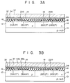
- Al-Si alloy layer 37 is formed on layer 34, as shown in Fig. 3A.
- Argon (Ar) for example, is then ion-implanted in the surface area of layer 37 at a dose of 5 x 1015 cm ⁇ 2 and an acceleration voltage of 30 keV. This causes the portion of layer 37 as extending to the dashed line (Fig. 3) to become amorphous.
- the remaining steps are the same as the steps above described.
- Ti in layer 34 becomes a nitride. This serves to control so that an Al-Si-Ti three-element alloy is not formed.
- Al-Si alloy layer 37 prevents alloy spikes, even if layer 34 has pinholes. Furthermore, since the surface crystal of layer 37 is broken through the Ar ion-implantation, the Al in layer 37 does not migrate along grain boundaries during the formation of layer 44. Thus, the generation of hillocks, electromigration, and thermal migration are prevented. With the device, the wiring is hardly be disconnected along Al grain boundaries. The amorphous portion of layer 37 absorbs stress when the layer 44 is formed.
- layer 37 may be replaced with Al layer 36.
- wiring electrodes 38A and 38B have a 3-layer structure of Al alloy layer 37 (or Al layer 36), TiN layer 34, and Ti layer 32.
- the electrodes may also have a Ti layer 50 between layers 37 and 34. With this structure, the Ti layer 50 prevents the diffusion of N from TiN layer 34 into Al alloy layer 37 (or Al layer 36). Ti diffuses from the Ti layer into layer 37 (or layer 36), thus preventing Al hillocks.
- Ar was ion-implanted in layer 37. It is also possible, however, to ion-implant As, BF2, or a mixture of the two.
- wiring electrodes 38A and 38B have a 3-layer structure formed of Al, TiN and Ti layers 36, 34, and 32.
- the electrodes 38A, 38B may have a 4-layer structure in which a TiSi layer 52 is further formed on top of Al layer 36 as shown in Fig. 5.
- the TiSi layer 52 blocks Al hillocks with the stress corresponding to their growth and allows diffusion of Ti into the Al or Al allow layer, thereby preventing hillocks. This Ti also plays a large role in the control of electromigration.
- the Ti, TiN, Al, and TiSi layers can all be deposited in the same vacuum.
Landscapes
- Internal Circuitry In Semiconductor Integrated Circuit Devices (AREA)
Applications Claiming Priority (5)
| Application Number | Priority Date | Filing Date | Title |
|---|---|---|---|
| JP100915/85 | 1985-05-13 | ||
| JP60100915A JPS61258452A (ja) | 1985-05-13 | 1985-05-13 | 半導体装置 |
| JP60196503A JPS6255929A (ja) | 1985-09-05 | 1985-09-05 | 半導体装置の製造方法 |
| JP196503/85 | 1985-09-05 | ||
| EP86106245A EP0209654B1 (de) | 1985-05-13 | 1986-05-07 | Halbleiteranordnung mit Verbindungselektroden |
Related Parent Applications (1)
| Application Number | Title | Priority Date | Filing Date |
|---|---|---|---|
| EP86106245.3 Division | 1986-05-07 |
Publications (2)
| Publication Number | Publication Date |
|---|---|
| EP0613180A2 true EP0613180A2 (de) | 1994-08-31 |
| EP0613180A3 EP0613180A3 (de) | 1994-10-19 |
Family
ID=26441855
Family Applications (2)
| Application Number | Title | Priority Date | Filing Date |
|---|---|---|---|
| EP9494108007A Ceased EP0613180A3 (de) | 1985-05-13 | 1986-05-07 | Halbleiteranordnung mit Verbindungselektroden. |
| EP86106245A Expired - Lifetime EP0209654B1 (de) | 1985-05-13 | 1986-05-07 | Halbleiteranordnung mit Verbindungselektroden |
Family Applications After (1)
| Application Number | Title | Priority Date | Filing Date |
|---|---|---|---|
| EP86106245A Expired - Lifetime EP0209654B1 (de) | 1985-05-13 | 1986-05-07 | Halbleiteranordnung mit Verbindungselektroden |
Country Status (2)
| Country | Link |
|---|---|
| EP (2) | EP0613180A3 (de) |
| DE (1) | DE3650170T2 (de) |
Families Citing this family (8)
| Publication number | Priority date | Publication date | Assignee | Title |
|---|---|---|---|---|
| NL8800359A (nl) * | 1988-02-15 | 1989-09-01 | Philips Nv | Werkwijze voor het vervaardigen van een halfgeleiderinrichting. |
| KR920005242A (ko) * | 1990-08-20 | 1992-03-28 | 김광호 | 게이트-절연체-반도체의 구조를 가지는 트랜지스터의 제조방법 |
| EP0517368B1 (de) * | 1991-05-03 | 1998-09-16 | STMicroelectronics, Inc. | Lokalverbindungen für integrierte Schaltungen |
| EP0514103A1 (de) * | 1991-05-14 | 1992-11-19 | STMicroelectronics, Inc. | Herstellungsverfahren von einer Metallbarriere für submikron Kontakte |
| JPH0730095A (ja) * | 1993-06-25 | 1995-01-31 | Mitsubishi Electric Corp | 半導体装置及びその製造方法 |
| KR0148325B1 (ko) * | 1995-03-04 | 1998-12-01 | 김주용 | 반도체 소자의 금속 배선 형성방법 |
| EP0732731A3 (de) * | 1995-03-13 | 1997-10-08 | Applied Materials Inc | Behandlung einer Titannitrid-Schicht zur Verbesserung der Beständigkeit gegen höhere Temperaturen |
| WO2018161100A1 (de) | 2017-03-07 | 2018-09-13 | Karl Angleitner | Lagerregal für Lagergüter und Regalbedieneinrichtung zum Ein- und Auslagern der Lagergüter |
Family Cites Families (2)
| Publication number | Priority date | Publication date | Assignee | Title |
|---|---|---|---|---|
| DE3217026A1 (de) * | 1981-05-06 | 1982-12-30 | Mitsubishi Denki K.K., Tokyo | Halbleitervorrichtung |
| JPS59231836A (ja) * | 1983-06-14 | 1984-12-26 | Toshiba Corp | 多層構造アルミニウム層の形成方法 |
-
1986
- 1986-05-07 EP EP9494108007A patent/EP0613180A3/de not_active Ceased
- 1986-05-07 EP EP86106245A patent/EP0209654B1/de not_active Expired - Lifetime
- 1986-05-07 DE DE3650170T patent/DE3650170T2/de not_active Expired - Lifetime
Also Published As
| Publication number | Publication date |
|---|---|
| EP0613180A3 (de) | 1994-10-19 |
| EP0209654A3 (en) | 1988-10-12 |
| EP0209654B1 (de) | 1994-12-14 |
| DE3650170T2 (de) | 1995-05-18 |
| DE3650170D1 (de) | 1995-01-26 |
| EP0209654A2 (de) | 1987-01-28 |
Similar Documents
| Publication | Publication Date | Title |
|---|---|---|
| US5278099A (en) | Method for manufacturing a semiconductor device having wiring electrodes | |
| US4551908A (en) | Process of forming electrodes and interconnections on silicon semiconductor devices | |
| EP0225920B1 (de) | Verfahren zur bildung von kontakten und gegenseitigen verbindungen für integrierte schaltungen | |
| US4392150A (en) | MOS Integrated circuit having refractory metal or metal silicide interconnect layer | |
| CA1204045A (en) | Cobalt silicide metallization for semiconductor transistors | |
| US5378652A (en) | Method of making a through hole in multi-layer insulating films | |
| US5217923A (en) | Method of fabricating a semiconductor device having silicided source/drain regions | |
| US5103272A (en) | Semiconductor device and a method for manufacturing the same | |
| JP3644983B2 (ja) | 半導体装置の低抵抗接触構造およびその形成方法 | |
| EP0174773A2 (de) | Halbleiteranordnung mit Verbindungsschichten | |
| US4663825A (en) | Method of manufacturing semiconductor device | |
| US4577396A (en) | Method of forming electrical contact to a semiconductor substrate via a metallic silicide or silicon alloy layer formed in the substrate | |
| JPH0750276A (ja) | 異なる導電型の領域の間の接合に低抵抗コンタクトを製造する方法 | |
| US5291058A (en) | Semiconductor device silicon via fill formed in multiple dielectric layers | |
| US4981816A (en) | MO/TI Contact to silicon | |
| US5413943A (en) | Semiconductor device and method of manufacturing the same | |
| EP0209654B1 (de) | Halbleiteranordnung mit Verbindungselektroden | |
| EP0769808A2 (de) | Nassätzverfahren mit hoher Selektivität zwischen Cu und Cu3Ge | |
| JPH0257707B2 (de) | ||
| US5521416A (en) | Semiconductor device having gate electrode and impurity diffusion layer different in conductivity type and method of manufacturing the same | |
| KR920009372B1 (ko) | 반도체장치의 제조방법 | |
| US6184098B1 (en) | Field effect transistor device and method of manufacturing the same | |
| US4954871A (en) | Semiconductor device with composite electrode | |
| JPH0653492A (ja) | 半導体装置及びその製造方法 | |
| JPH0697667B2 (ja) | 半導体装置の製造方法 |
Legal Events
| Date | Code | Title | Description |
|---|---|---|---|
| PUAI | Public reference made under article 153(3) epc to a published international application that has entered the european phase |
Free format text: ORIGINAL CODE: 0009012 |
|
| PUAL | Search report despatched |
Free format text: ORIGINAL CODE: 0009013 |
|
| 17P | Request for examination filed |
Effective date: 19940524 |
|
| AC | Divisional application: reference to earlier application |
Ref document number: 209654 Country of ref document: EP |
|
| AK | Designated contracting states |
Kind code of ref document: A2 Designated state(s): DE FR GB |
|
| RHK1 | Main classification (correction) |
Ipc: H01L 23/48 |
|
| AK | Designated contracting states |
Kind code of ref document: A3 Designated state(s): DE FR GB |
|
| 17Q | First examination report despatched |
Effective date: 19970820 |
|
| STAA | Information on the status of an ep patent application or granted ep patent |
Free format text: STATUS: THE APPLICATION HAS BEEN REFUSED |
|
| 18R | Application refused |
Effective date: 20000118 |