EP0613273A2 - Système de commutation de paquets - Google Patents
Système de commutation de paquets Download PDFInfo
- Publication number
- EP0613273A2 EP0613273A2 EP94301268A EP94301268A EP0613273A2 EP 0613273 A2 EP0613273 A2 EP 0613273A2 EP 94301268 A EP94301268 A EP 94301268A EP 94301268 A EP94301268 A EP 94301268A EP 0613273 A2 EP0613273 A2 EP 0613273A2
- Authority
- EP
- European Patent Office
- Prior art keywords
- packet
- arrival time
- time information
- packets
- accumulating
- Prior art date
- Legal status (The legal status is an assumption and is not a legal conclusion. Google has not performed a legal analysis and makes no representation as to the accuracy of the status listed.)
- Granted
Links
Images



Classifications
-
- H—ELECTRICITY
- H04—ELECTRIC COMMUNICATION TECHNIQUE
- H04Q—SELECTING
- H04Q11/00—Selecting arrangements for multiplex systems
- H04Q11/04—Selecting arrangements for multiplex systems for time-division multiplexing
- H04Q11/0428—Integrated services digital network, i.e. systems for transmission of different types of digitised signals, e.g. speech, data, telecentral, television signals
- H04Q11/0478—Provisions for broadband connections
-
- H—ELECTRICITY
- H04—ELECTRIC COMMUNICATION TECHNIQUE
- H04L—TRANSMISSION OF DIGITAL INFORMATION, e.g. TELEGRAPHIC COMMUNICATION
- H04L49/00—Packet switching elements
- H04L49/15—Interconnection of switching modules
- H04L49/1507—Distribute and route fabrics, e.g. sorting-routing or Batcher-Banyan
-
- H—ELECTRICITY
- H04—ELECTRIC COMMUNICATION TECHNIQUE
- H04L—TRANSMISSION OF DIGITAL INFORMATION, e.g. TELEGRAPHIC COMMUNICATION
- H04L49/00—Packet switching elements
- H04L49/30—Peripheral units, e.g. input or output ports
- H04L49/3018—Input queuing
-
- H—ELECTRICITY
- H04—ELECTRIC COMMUNICATION TECHNIQUE
- H04L—TRANSMISSION OF DIGITAL INFORMATION, e.g. TELEGRAPHIC COMMUNICATION
- H04L49/00—Packet switching elements
- H04L49/30—Peripheral units, e.g. input or output ports
- H04L49/3027—Output queuing
Definitions
- the present invention relates generally to a packet switching system. More specifically, the invention relates to a packet switching technology in a digital communication network employing a packet.
- the first stage packet switch does not perform a path selection for the input packet and the input packet is uniformly supplied to subsequent stages of packet switch regardless of its address information and path selection is performed in the subsequent stages of packet switch for simplification of a path selection control and for preventing an internal blocking (which means a condition wherein call cannot be connected due to blocking of an internal link despite of presence of vacant capacity in the incoming and outgoing channels).
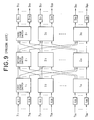
- Fig. 9 shows the block diagram of the conventional system.
- the switching system is constituted of three stages of switches, as shown in Fig. 9 . Eight each of input ports 711 ⁇ 788 are provided for each of the first stage switches and eight each of output ports 911 ⁇ 988 are provided for each of the third stage switches.
- Time stamping circuit 411 ⁇ 488 are provided for each of input ports and packet buffer circuit 511 ⁇ 588 are also provided for each of output ports.
- the time stamping circuit provides a time stamp representing input time information for each of packets input at an input port.
- Each of input packets is distributed to respective second stage switches 21 ⁇ 28 by the first stage switch regardless of address information, and then switched to desired destination per packet by the second stage switches 21 ⁇ 28 and third stage switches 31 ⁇ 38 . After having passed through switches, the packets are once stored in packet sorting circuits 511 ⁇ 588 which are provided at outlets of the third stage of switches 31 ⁇ 38 .
- Those stored packet are output to output ports 911 ⁇ 988 in accordance with the time information order of a period longer than a predetermined period of time (a possible maximum delay period required for passing through the first stage switches 11 ⁇ 18 to the third stage switches 31 ⁇ 38 ) and whereby each of the packets of the same cell is arranged in order.
- the delay period of the packet is inherently increased since the packet buffer circuits delay the packet for a period longer than the predetermined period of time.
- Another object of the invention is to provide a packet switching system which can simplify the hardware necessary for controlling the arrangement of the packets in order.
- a packet switching system comprises: a plurality of incoming channels, through which packets arrive; time information providing means for providing arrival time information for inclusion in headers of respective packets; copying means for copying said arrival time information in the headers of respective packets; arrival time information accumulating means for accumulating the copied arrival time information in order of the arrival time; packet accumulating means for accumulating said packets having time information in their headers in order of the arrival time; control means for outputting the packets accumulated in said packet accumulating means and having arrival time information consistent with the arrival time information accumulated at the leading end of said arrival time information accumulating means; first switching means for routing the packets output from said packet accumulating means according to destinations contained in the headers thereof; and a plurality of outgoing channels for feeding out the routed packets.
- the packet switching system further comprises second switching means for routing respective packets provided with the arrival time information depending upon the destinations contained in the header information thereof, and each packet routed by the second switching means is supplied to the packet accumulating means corresponding to the route.
- the control means may comprise: first detection means for detecting absence of input for each packet accumulating means corresponding to the route; second detection means for detecting the presence of one or more packets in each said packet accumulating means, and output control for each accumulated packet of said packet accumulating means is performed depending upon the results of detection by said first and second detection means.
- a packet switching system including a plurality of incoming channels, through which packets arrive, means for providing arrival time information for headers of respective packets, switching means for routing the packets according to destinations contained in the headers thereof, means for sorting the routed packets according to the order of arrival time information, and a plurality of outgoing channels for feeding out the packets sorted by said sorting means, said system comprising: copying means for copying respective of said arrival time information provided in headers of respective packets; and means for transferring the arrival time information copied by said copying means to said sorting means, said sorting means including: means for accumulating the transferred arrival time information in an order of the arrival time; means for outputting the packets having the arrival time information consistent with the arrival time information at the leading end of said accumulating means.
- the copying means includes means for counting the number of packets having the same arrival time information
- the transferring means includes means for transferring the counted number with the associated arrival time information
- the sorting means includes means for storing the counted number and establishing correspondence with the arrival time information and means for updating said number stored in said storage means by subtracting one on each outputting of a packet having a header containing said same arrival time information.
- Fig. 1 shows the block diagram of one embodiment of a packet switching system in accordance with the present invention.
- Fig. 1 there is provided 64 incoming channels 711 ⁇ 788 , through which packets arrive.
- incoming channels 711 ⁇ 788 For routing the packets, input through the incoming channels 711 ⁇ 788 , to respective destinations according to the header information of respective packets, crosslinked first stage switches 11 ⁇ 18 , second stage switches 21 ⁇ 28 and third stage switches 31 ⁇ 38 are provided in this order.
- the first stage switches 11 ⁇ 18 respective comprise time stamping portions 141 ⁇ 148 and packet distributing portions 611 ⁇ 618 .
- the time stamping portions provide arrival time information to the header information of respective input packets.
- Each packet distributing portion is a distributing switch to which input and output are connected in one-to-one relationship for varying states of connection.
- the second stage switches 21 ⁇ 28 comprise respectively address and time stamp detecting portions 81 ⁇ 88 and packet switching portions 621 ⁇ 628 .
- the address/time stamp detecting portions detect the arrival time information contained in the header information of respective packets and copy the detected information.
- Each packet switching portion switches each of packets without changing order of arrival.
- the third stage switch 31 ⁇ 38 comprise packet sorting portions 151 ⁇ 158 and packet switching portions 31 ⁇ 38 .
- the packet sorting portions arrange and store the arrival time information transferred from the second stage switches 21 ⁇ 28 in the order of the arrival time.
- the packet sorting portions perform rearrangement of the received packets with reference to the arrival time information, and output the packet, whose arrival time information in the header coincides with the arrival time information stored in the leading end of the packet storing portion, to the third packet switching portion 631.
- the packet switching portions 631 ⁇ 638 have the same construction and function as those of the packet switching portions 621 ⁇ 628 .
- Respective of the output packets of the third stage switch 31 ⁇ 38 are fed to the outgoing channels 911 ⁇ 988 .
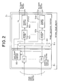
- FIG. 2 is a block diagram of the second stage switch 21 of the shown embodiment of the packet switching system of the invention.
- Fig. 3 is a block diagram of the third stage switch 31 of the shown embodiment of the invention.
- Figs. 4 and 5 are illustrations showing operation of the shown embodiment of the packet switching system of the invention.
- the time stamp, arrival time information is provided for the header information of the packet input through the incoming channels 711 ⁇ 718 by the time stamping portion 141 .
- the packets are distributed to eight output routes by the packet distributing portions 611 ⁇ 618 for outputting to the second stage switch 21 .
- address and time stamp detecting circuits 181 ⁇ 188 of the address and time stamp detecting portion 81 of the second stage switch 21 address and time stamp are copied from the header information of the input packet.
- the copied time stamp is transferred to one of the third stage switches 31 ⁇ 38 which accommodates one of outgoing channels 911 ⁇ 988 corresponding to the address by a time stamp feeding circuit 80 .
- the packet past through the address and time stamp detecting circuit 181 ⁇ 188 is temporarily stored in packet buffer 641 ⁇ 648 corresponding to the address in the header information which is detected by address filter 621 ⁇ 628 via a time division multiplexing bus 60 , and then output to respective third stage switches 31 ⁇ 38 .
- the packet buffer 641 ⁇ 648 are adapted to output empty packets to the third stage switch 31 ⁇ 38 when no packet is accumulated therein.
- the time stamps transferred from the second stage switches 21 ⁇ 28 are accumulated in a time stamp buffer 55 in the order of arrival.
- a time stamp detecting circuit 51 accumulates those time stamps as a single stamp in the time stamp buffer 55 . Since these time stamps do not pass any intermediate buffer, they are accumulated in the time stamp buffer 55 with maintaining the order of input.
- the packets transferred from the packet buffers 641 ⁇ 648 of the second stage switches 21 ⁇ 28 are accumulated in the packet sorting buffers 521 ⁇ 528 in the third stage switch 31 .
- the packets accumulated in the packet sorting buffers 521 ⁇ 528 are output to a multiplexing circuit 58 without destructing the order under the control of an empty packet detecting portions 501 ⁇ 508 , a buffer condition monitoring portion 54 and a time stamp comparing portion 56 .
- the empty packet detection portions 501 ⁇ 508 are provided corresponding to respective inputs of the packet sorting buffers 521 ⁇ 528 for detecting that the packets input from the second stage switches 21 ⁇ 28 are empty and to report to the buffer condition monitoring portion 54. Namely, each of the empty packet detecting portions 501 to 508 detects the fact that no packet is transferred from the packet buffers 641 ⁇ 648 of the second stage switch.
- the packet condition monitoring portion 54 monitors the packet accumulating condition of respective buffers 521 ⁇ 528 to output a comparison enabling signal to a time stamp comparing portion 56 according to the packet accumulating condition and the result of detection by the empty packet detecting portions 501 ⁇ 508 .
- the buffer condition monitoring portion 54 outputs the comparison enabling signal to the comparing portion 56 when the fact that no packet is present in the second stage switch corresponding to the empty packet sorting buffer is detected by the empty packet detecting portions 501 ⁇ 508 .
- the buffer condition monitoring portion 54 outputs the comparison enabling signal to the time stamp comparing portion 56 .
- the time stamp comparing portion 56 compares the time of the leading time stamp among those accumulated in the time stamp buffer 55 and the time of the time stamp given for the leading packet of the packet sorting buffers 521 ⁇ 528 to perform control for feeding the packet, time stamp of which matches with that of the leading time stamp in the time stamp buffer 55 , to the multiplexing circuit 58 .
- the leading time stamp of the time stamp buffer 55 is disposed and the next time stamp is shifted up to be the leading time stamp.
- the packets are transferred to the multiplexing circuit 58 .
- the output of the multiplexing circuit 58 is input to the packet switching portion 631 .
- the packets are distributed depending on destinations by the address filters 621 ⁇ 628 and then accumulated in the packet buffers 641 ⁇ 648 .
- the packets accumulated in the packet buffers 641 ⁇ 648 are fed out to the outgoing channels 911 ⁇ 918
- the operation of the third stage switch 31 is illustrated for better understanding in Figs.4 and 5 .
- the time of the leading time stamp of the time stamp buffer 55 is 4, and the time stamp provided for the leading packet of the packet sorting buffer 521 is also 4. Accordingly, the packet provided the time stamp 4 is output to the multiplexing circuit 58 .
- the packet having the time stamp consistent with the time 4 of the time stamp of the leading time stamp in the time stamp buffer 55 is not present any more in the packet sorting buffer 521 ⁇ 528 . Therefore, the time stamp having the time 4 is disposed.
- Fig. 6 is a block diagram of the second stage switch 21 in the second embodiment of the invention.
- Fig. 7 is a block diagram of the third stage switch 31 in the second embodiment of the invention.
- Fig. 8 is an illustration showing the operation of the second embodiment of the packet switching system according to the invention.
- the packets transferred from the first stage switches 11 ⁇ 18 are accumulated in the packet buffers 641 ⁇ 648 with distribution by the address filters 621 ⁇ 628 via the time division multiplexing bus 60 .
- the time stamps provided in the header information of the packets are copied by the address and time stamp detecting portion 81 .
- the packet number computing circuits 821 ⁇ 828 counts the number of time stamps of the same time. The time information of the time stamps and the number information of the time stamps having the same time are transferred to the third stage switches 31 ⁇ 3 8 .
- the time stamp comparing circuit 56 compares the time of the time stamps of the leading packets in the packets accumulated in the packet sorting buffer 521 ⁇ 528 and the time of the time stamp accumulated in the time stamp buffer 55 .
- Number of the leading time stamp of the time stamps of the time stamp buffer 55 is accumulated in the packet number buffer 59 corresponding to the leading time stamp.
- the consistent time stamp When the consistent time stamp is present, such packets are fed out from the packet sorting buffer 521 ⁇ 528 . Then, the number of the fed out packets is decremented from the value in the packet number buffer 59 by a packet decrementing circuit 57 . When the number of the leading time stamps accumulated at the leading portions becomes "0", the leading time stamp of the time stamp buffer 55 is disposed. Then, the next time stamp is shifted to be the leading time stamp for repeating the operation set forth above.
- the packet sorting buffers 521 ⁇ 528 send a notice to the second stage switch 21 to stop outputting of the packet when the packet sorting buffers 521 ⁇ 528 have no vacancy.
- the packet sorting portion 151 can detect the number of packets having the time stamps of the same arrival time. By this, it becomes possible to avoid occurrence of excluding a packet, which has the not yet arrived from packet sorting procedure even when packet sorting procedure is initiated before all packets arrive. Therefore, further higher speed packet switching system than the former, first embodiment can be realized.
- FIFO First in First out memory
- the internal blocking can be avoided by eliminating necessity of preliminary routing and a period required for sorting the packet-can be shortened.
- the control necessary for sorting the packet can be simplified.
Landscapes
- Engineering & Computer Science (AREA)
- Computer Networks & Wireless Communication (AREA)
- Signal Processing (AREA)
- Data Exchanges In Wide-Area Networks (AREA)
Applications Claiming Priority (3)
| Application Number | Priority Date | Filing Date | Title |
|---|---|---|---|
| JP3366393 | 1993-02-23 | ||
| JP33663/93 | 1993-02-23 | ||
| JP3366393A JPH0775353B2 (ja) | 1993-02-23 | 1993-02-23 | パケット交換方式 |
Publications (3)
| Publication Number | Publication Date |
|---|---|
| EP0613273A2 true EP0613273A2 (fr) | 1994-08-31 |
| EP0613273A3 EP0613273A3 (en) | 1996-08-07 |
| EP0613273B1 EP0613273B1 (fr) | 2002-06-19 |
Family
ID=12392699
Family Applications (1)
| Application Number | Title | Priority Date | Filing Date |
|---|---|---|---|
| EP94301268A Expired - Lifetime EP0613273B1 (fr) | 1993-02-23 | 1994-02-23 | Système de commutation de paquets |
Country Status (5)
| Country | Link |
|---|---|
| US (1) | US5402417A (fr) |
| EP (1) | EP0613273B1 (fr) |
| JP (1) | JPH0775353B2 (fr) |
| CA (1) | CA2116308C (fr) |
| DE (1) | DE69430828T2 (fr) |
Cited By (2)
| Publication number | Priority date | Publication date | Assignee | Title |
|---|---|---|---|---|
| EP0724344A3 (fr) * | 1995-01-30 | 1998-08-19 | McData Corporation | Système et procédé à haute performance de surveillance du temps de trame pour un commutateur à fibres optiques pour réseau à fibres optiques |
| EP0701348A3 (fr) * | 1994-09-09 | 1999-08-04 | Philips Patentverwaltung GmbH | Système de transmission de paquets |
Families Citing this family (12)
| Publication number | Priority date | Publication date | Assignee | Title |
|---|---|---|---|---|
| JP3544390B2 (ja) * | 1994-06-29 | 2004-07-21 | 富士通株式会社 | 並列計算機で用いられるメッセージ通信方法 |
| US5666348A (en) * | 1995-09-18 | 1997-09-09 | Telefonaktiebolaget L M Ericsson (Publ.) | Packet switched radio channel admission control in a cellular telecommunications system |
| US5689508A (en) * | 1995-12-21 | 1997-11-18 | Xerox Corporation | Reservation ring mechanism for providing fair queued access in a fast packet switch networks |
| US5878045A (en) * | 1996-04-26 | 1999-03-02 | Motorola, Inc. | Method and apparatus for converting data streams in a cell based communications system |
| US5867488A (en) * | 1996-06-30 | 1999-02-02 | Motorola, Inc. | Digital multi-channel simulcast system with centralized timestamping device |
| JP3589851B2 (ja) * | 1998-02-20 | 2004-11-17 | 株式会社日立製作所 | パケット通信システム及びパケット通信装置 |
| US6247058B1 (en) * | 1998-03-30 | 2001-06-12 | Hewlett-Packard Company | Method and apparatus for processing network packets using time stamps |
| CA2308184A1 (fr) * | 1998-06-11 | 1999-12-16 | Synchrodyne Inc. | Commutation de paquets avec reference de temps commune |
| EP0982970B1 (fr) | 1998-08-21 | 2006-10-04 | Nippon Telegraph and Telephone Corporation | Commutateur ATM |
| JP4294821B2 (ja) | 2000-01-26 | 2009-07-15 | 株式会社日立製作所 | ネットワーク中継装置 |
| US6757284B1 (en) * | 2000-03-07 | 2004-06-29 | Cisco Technology, Inc. | Method and apparatus for pipeline sorting of ordered streams of data items |
| US7336667B2 (en) * | 2002-11-21 | 2008-02-26 | International Business Machines Corporation | Apparatus, method and program product to generate and use CRC in communications network |
Family Cites Families (7)
| Publication number | Priority date | Publication date | Assignee | Title |
|---|---|---|---|---|
| US4551833A (en) * | 1983-08-10 | 1985-11-05 | At&T Bell Laboratories | Distributed monitoring of packet transmission delay |
| US4899335A (en) * | 1988-12-21 | 1990-02-06 | American Telephone And Telegraph Company, At&T Bell Laboratories | Self routing packet switching network architecture |
| WO1991002419A1 (fr) * | 1989-08-09 | 1991-02-21 | Alcatel N.V. | Systeme de remise en sequence pour n×ud de commutation |
| US4991171A (en) * | 1989-09-26 | 1991-02-05 | At&T Bell Laboratories | Broadcast packet switch network |
| IT1237302B (it) * | 1989-11-30 | 1993-05-27 | Vinicio Vercellone | Elemento base per la rete di connessione di un nodo di commutazione veloce di cella. |
| US5260935A (en) * | 1991-03-01 | 1993-11-09 | Washington University | Data packet resequencer for a high speed data switch |
| US5274642A (en) * | 1992-06-05 | 1993-12-28 | Indra Widjaja | Output buffered packet switch with a flexible buffer management scheme |
-
1993
- 1993-02-23 JP JP3366393A patent/JPH0775353B2/ja not_active Expired - Fee Related
-
1994
- 1994-02-18 US US08/198,266 patent/US5402417A/en not_active Expired - Lifetime
- 1994-02-22 CA CA002116308A patent/CA2116308C/fr not_active Expired - Fee Related
- 1994-02-23 EP EP94301268A patent/EP0613273B1/fr not_active Expired - Lifetime
- 1994-02-23 DE DE69430828T patent/DE69430828T2/de not_active Expired - Fee Related
Cited By (2)
| Publication number | Priority date | Publication date | Assignee | Title |
|---|---|---|---|---|
| EP0701348A3 (fr) * | 1994-09-09 | 1999-08-04 | Philips Patentverwaltung GmbH | Système de transmission de paquets |
| EP0724344A3 (fr) * | 1995-01-30 | 1998-08-19 | McData Corporation | Système et procédé à haute performance de surveillance du temps de trame pour un commutateur à fibres optiques pour réseau à fibres optiques |
Also Published As
| Publication number | Publication date |
|---|---|
| DE69430828T2 (de) | 2002-10-02 |
| JPH0775353B2 (ja) | 1995-08-09 |
| EP0613273B1 (fr) | 2002-06-19 |
| EP0613273A3 (en) | 1996-08-07 |
| US5402417A (en) | 1995-03-28 |
| CA2116308A1 (fr) | 1994-08-24 |
| CA2116308C (fr) | 1999-10-12 |
| DE69430828D1 (de) | 2002-07-25 |
| JPH06252948A (ja) | 1994-09-09 |
Similar Documents
| Publication | Publication Date | Title |
|---|---|---|
| AU675302B2 (en) | Output-buffer switch for asynchronous transfer mode | |
| US6907001B1 (en) | Packet switch for switching variable length packets in the form of ATM cells | |
| US5287535A (en) | Switching node in label multiplexing type switching network | |
| EP0494170B1 (fr) | Noeud de commutation pour reseau de commutation de communications | |
| US6259696B1 (en) | ATM switch and congestion control method | |
| US6011779A (en) | ATM switch queuing system | |
| US5663959A (en) | ATM cell switching apparatus having a control cell bypass route | |
| US6041038A (en) | Packet switching device and cell transfer control method | |
| US5200950A (en) | Method and circuit arrangement for reducing the loss of message packets that are transmitted via a packet switching equipment | |
| EP0613273B1 (fr) | Système de commutation de paquets | |
| US6052376A (en) | Distributed buffering system for ATM switches | |
| JPH07202942A (ja) | パケット交換機 | |
| US5398235A (en) | Cell exchanging apparatus | |
| JP3632229B2 (ja) | Atm交換装置 | |
| EP0339809B1 (fr) | Réseau à division temporelle asynchrone | |
| US20120224473A1 (en) | Header conversion technique | |
| EP0866632A2 (fr) | Système de multiplexage de lignes | |
| EP0612171A2 (fr) | Dispositif de file d'attente de données et commutateur de cellules ATM par décalage et recherche | |
| US6144642A (en) | Signal transfer device in a telecommunications network | |
| WO2000079739A1 (fr) | Dispositif et procede de mise en file d'attente de donnees | |
| GB2306076A (en) | ATM network switch | |
| CA2090101C (fr) | Appareil d'echange cellulaire | |
| US5818837A (en) | ATM cell switching network | |
| JP3011155B2 (ja) | パケットセル廃棄制御装置 | |
| JP2876859B2 (ja) | パケット交換方式 |
Legal Events
| Date | Code | Title | Description |
|---|---|---|---|
| PUAI | Public reference made under article 153(3) epc to a published international application that has entered the european phase |
Free format text: ORIGINAL CODE: 0009012 |
|
| AK | Designated contracting states |
Kind code of ref document: A2 Designated state(s): DE FR GB |
|
| PUAL | Search report despatched |
Free format text: ORIGINAL CODE: 0009013 |
|
| AK | Designated contracting states |
Kind code of ref document: A3 Designated state(s): DE FR GB |
|
| 17P | Request for examination filed |
Effective date: 19960703 |
|
| GRAG | Despatch of communication of intention to grant |
Free format text: ORIGINAL CODE: EPIDOS AGRA |
|
| 17Q | First examination report despatched |
Effective date: 20010924 |
|
| GRAG | Despatch of communication of intention to grant |
Free format text: ORIGINAL CODE: EPIDOS AGRA |
|
| GRAH | Despatch of communication of intention to grant a patent |
Free format text: ORIGINAL CODE: EPIDOS IGRA |
|
| GRAH | Despatch of communication of intention to grant a patent |
Free format text: ORIGINAL CODE: EPIDOS IGRA |
|
| GRAA | (expected) grant |
Free format text: ORIGINAL CODE: 0009210 |
|
| AK | Designated contracting states |
Kind code of ref document: B1 Designated state(s): DE FR GB |
|
| REG | Reference to a national code |
Ref country code: GB Ref legal event code: FG4D |
|
| REF | Corresponds to: |
Ref document number: 69430828 Country of ref document: DE Date of ref document: 20020725 |
|
| ET | Fr: translation filed | ||
| PLBE | No opposition filed within time limit |
Free format text: ORIGINAL CODE: 0009261 |
|
| STAA | Information on the status of an ep patent application or granted ep patent |
Free format text: STATUS: NO OPPOSITION FILED WITHIN TIME LIMIT |
|
| 26N | No opposition filed |
Effective date: 20030320 |
|
| PGFP | Annual fee paid to national office [announced via postgrant information from national office to epo] |
Ref country code: DE Payment date: 20070215 Year of fee payment: 14 |
|
| PGFP | Annual fee paid to national office [announced via postgrant information from national office to epo] |
Ref country code: GB Payment date: 20070221 Year of fee payment: 14 |
|
| PGFP | Annual fee paid to national office [announced via postgrant information from national office to epo] |
Ref country code: FR Payment date: 20070208 Year of fee payment: 14 |
|
| GBPC | Gb: european patent ceased through non-payment of renewal fee |
Effective date: 20080223 |
|
| REG | Reference to a national code |
Ref country code: FR Ref legal event code: ST Effective date: 20081031 |
|
| PG25 | Lapsed in a contracting state [announced via postgrant information from national office to epo] |
Ref country code: DE Free format text: LAPSE BECAUSE OF NON-PAYMENT OF DUE FEES Effective date: 20080902 |
|
| PG25 | Lapsed in a contracting state [announced via postgrant information from national office to epo] |
Ref country code: FR Free format text: LAPSE BECAUSE OF NON-PAYMENT OF DUE FEES Effective date: 20080229 |
|
| PG25 | Lapsed in a contracting state [announced via postgrant information from national office to epo] |
Ref country code: GB Free format text: LAPSE BECAUSE OF NON-PAYMENT OF DUE FEES Effective date: 20080223 |