EP0613574B1 - Additionneur numerique ayant un chemin de signaux de derivation de report a haute vitesse et faible capacitance - Google Patents
Additionneur numerique ayant un chemin de signaux de derivation de report a haute vitesse et faible capacitance Download PDFInfo
- Publication number
- EP0613574B1 EP0613574B1 EP92925283A EP92925283A EP0613574B1 EP 0613574 B1 EP0613574 B1 EP 0613574B1 EP 92925283 A EP92925283 A EP 92925283A EP 92925283 A EP92925283 A EP 92925283A EP 0613574 B1 EP0613574 B1 EP 0613574B1
- Authority
- EP
- European Patent Office
- Prior art keywords
- carry
- digital adder
- terminal
- thru
- transistor
- Prior art date
- Legal status (The legal status is an assumption and is not a legal conclusion. Google has not performed a legal analysis and makes no representation as to the accuracy of the status listed.)
- Expired - Lifetime
Links
Images


Classifications
-
- G—PHYSICS
- G06—COMPUTING OR CALCULATING; COUNTING
- G06F—ELECTRIC DIGITAL DATA PROCESSING
- G06F7/00—Methods or arrangements for processing data by operating upon the order or content of the data handled
- G06F7/38—Methods or arrangements for performing computations using exclusively denominational number representation, e.g. using binary, ternary, decimal representation
- G06F7/48—Methods or arrangements for performing computations using exclusively denominational number representation, e.g. using binary, ternary, decimal representation using non-contact-making devices, e.g. tube, solid state device; using unspecified devices
- G06F7/50—Adding; Subtracting
- G06F7/505—Adding; Subtracting in bit-parallel fashion, i.e. having a different digit-handling circuit for each denomination
- G06F7/506—Adding; Subtracting in bit-parallel fashion, i.e. having a different digit-handling circuit for each denomination with simultaneous carry generation for, or propagation over, two or more stages
-
- G—PHYSICS
- G06—COMPUTING OR CALCULATING; COUNTING
- G06F—ELECTRIC DIGITAL DATA PROCESSING
- G06F2207/00—Indexing scheme relating to methods or arrangements for processing data by operating upon the order or content of the data handled
- G06F2207/38—Indexing scheme relating to groups G06F7/38 - G06F7/575
- G06F2207/3804—Details
- G06F2207/386—Special constructional features
- G06F2207/3876—Alternation of true and inverted stages
Definitions
- This invention relates to the structure of digital circuits which add binary data bits; and more particularly, it relates to the structure of such adder circuits which operate at high speed.
- digital adder circuits have been widely used. For example, they are used in the arithmetic units of general purpose digital computers, and they are also used in special purpose arithmetic modules such as a multiplier. In many of these applications, the speed at which the adder circuit operates is of critical importance.
- FIG. 5 shows a circuit diagram of a digital adder in which the signal path from the carry-in signal for the least significant bits, to the carry-out terminal from the most significant bits, goes through one input inverter and the channels of several transistors and one output inverter. A separate transistor channel is included for each pair of data bits being added.
- This adder circuit avoids the time delay through a serial string of logic gates by replacing it with a shorter time delay through a serial string of transistor channels.
- Gotto's Fig. 3 embodiment includes three bypass circuits #1', #2', and #3'. In the case where each of those bypass circuits is active, the initial carry-in signal C 0 travels through a first carry circuit #1, then through bypass circuit #1', then through bypass circuit #2', and then through a last carry circuit #(L+2).
- the carry-in signal C 0 also travels through other circuits. Specifically, the carry-in signal C 0 travels through all of the carry circuits #2 - #m, then through bypass circuit #3', and then through carry circuits #1-#(m+2). Each of those circuits has an inherent capacitance associated with the channel of a transistor (labeled 1 in Fig. 4a), and the total capacitance from those transistors in all of the circuits #2-#m, #3', and #1-#(m+2) is coupled to the output terminal of circuit #1. Consequently, the propagation delay from circuit #1 to circuit #1' is slowed down.
- the bypass path for the carry-in signal C i-1 goes through the channel of a bypass transistor (labeled 2) and through an inverter (not labeled) to form the carry-out signal C
- the carry-in signal C i-1 also goes through the channel of an extra transistor (labeled 1) to the input of an extra inverter (not labeled); and, the output from the channel of the bypass transistor 2 goes to the channel of another extra transistor (labeled 1). All of these extra components add capacitance to the bypass path, and that slows down the speed at which signals propagate along the bypass path.
- Gotto's embodiments are incomplete in that they do not form any sum bits from the carry signals. To form those sum bits, EXCLUSIVE-OR gates need to be coupled to the channels of each of the transistors 1, and that adds even more capacitance to the bypass path. For example, in Gotto's Fig. 7B embodiment, one EXCLUSIVE-OR gate would be added to the input of the leftmost transistor 1 and another EXCLUSIVE-OR gate would be added to the input of the rightmost transistor 1.
- FIG. 1 An overall block diagram of the Robertson et al adder is shown in Fig. 1 as a set of 16 identical stages which are interconnected in series.
- Fig. 3 is a detailed circuit diagram of one of the stages which shows each stage operates on two data bits.
- a carry signal must always propagate in a serial fashion from the first stage all the way to the last stage. In other words, one intermediate stage in the series will not generate a carry on its own to the next stage; and that in turn makes the adder operate slowly.
- the Robertson et al adder in each stage, the carry-out terminal must be precharged to a high level before any data can be added. Consequently, the overall cycle time at which the Robertson et al adder can be used is long because that cycle time must include the time that it takes for all of the stages to perform an add plus the time that it takes to precharge those stages. Further, still another drawback of the Robertson et al adder is that the carry path which runs in a serial fashion through all of the stages includes a large number of components; and that in turn forces the delay of the carry path to be long. In particular, for each pair of stages (i.e.
- the carry path includes the channel of two transistors plus the capacitance which is associated with the source and/or drain of eight other transistors.
- a primary object of the invention is to provide a digital adder circuit which overcomes the above described prior art problems and which operates faster than the prior art adders.
- a digital adder module which uses the present invention as defined in claim 1, has data input terminals for receiving N pairs of data bit signals A 1 and B 1 thru A N and B N , a carry-in terminal for receiving a carry-in signal, sum output terminals on which N sum bits are generated, and a carry-out terminal.
- multiple modules are intercoupled in series with a respective inverter between the carry-out terminal and the carry-in terminal of successive modules.
- each module includes: a) a quasi carry circuit which generates a quasi carry-out signal that is valid only when the data bits of at least one of the N data bit pairs are equal, and which presents no load to the carry-in signal; b) a control circuit which generates a first control signal indicating when the data bits of at least one of the N data bit pairs are equal, which generates a second control signal that is the inverse of the first control signal, and which presents no load to the carry-in signal; c) a first transistor having a source connected to receive the quasi carry-out signal, a drain connected to the carry-out terminal, and a gate which receives the first control signal; d) a second transistor having a source connected to the carry-in terminal, a drain connected to the carry-out terminal, and a gate which receives the second control signal; and, e) a summing circuit which generates the sum bits from the data bits and the carry-in signal, and which presents a load of only a single invert
- C IN C CH + C DR , + C SUM + C LOAD + C WIRE .
- C CH is the channel capacitance of the second transistor
- C DR is the drain capacitance of the first transistor
- C SUM is the input capacitance of the single inverter in the summing circuit
- C LOAD is the capacitance of the inverter between two successive modules
- C WIRE is the capacitance of the interconnections between the identified components.
- the capacitance C IN is small, and thus signals propagate from the carry-in terminal to the carry-out terminal with a high speed.
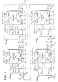
- the adder is a sixteen bit adder which is comprised of four modules M1, M2, M3, and M4.
- Modules M1 and M3 are identical in structure, and their internal circuits are shown in detail in Fig. 2.
- Modules M2 and M4 are also identical in structure, and their internal circuits are shown in detail in Fig. 3.
- Module M1 has data input terminals 10 and 11, and it has a carry-in terminal 12.
- Four data bit signals A 4 -A 1 are received on the input terminals 10;
- four data bit signals B 4 -B 1 are received on the input terminals 11; and
- a single carry-in signal CI 1 is received on the input terminal 12.
- a high voltage level e.g. - 5 volts
- a low voltage level e.g. - 0 volts
- Signals A1 and B1 are the least significant bits; signals A2 and B2 are the next least significant bits; etc.
- Module M1 further includes a quasi carry-out circuit 13, a control circuit 14, and a summing circuit 15.
- the quasi carry-out circuit 13 generates a quasi carry-out signal QCO 4 on a conductor 13a.
- Signal QCO 4 indicates the carry that is produced when just the data bits A 4 -A 1 and B 4 -B 1 are added (the carry-in signal on terminal 12 is ignored).
- Signal QCO 4 is valid only when at least one of the data bit pairs A 1 and B 1 , A 2 and B 2 , etc. are equal. For that case, a carry having a binary value of "1" is indicated by signal QCO 4 being a high voltage, and a binary value of "0" is indicated by a low voltage.
- Control circuit 14 generates two control signals CA 4 and CB 4 on conductors 14a and 14b respectively. These control signals are functions of just the data bits on terminals 10 and 11, and not the carry-in signal on terminal 12. Specifically, signal CA 4 is high whenever at least one of the data bit pairs A 1 and B 1 , A 2 and B 2 , etc. are equal, and control signal CB 4 is the inverse of control signal CA 4 .
- Summing circuit 15 operates on the data bits on terminals 10 and 11 as well as the carry-in signal on terminal 12 to generate sum bits S 4 thru S 1 .
- S 1 is the least significant sum bit;
- S 2 is the next least significant sum bit; etc.
- circuit 15 utilizes an inverter 15a as the only load that circuit 15 presents to the carry-in signal on terminal 12.
- Transistor T10 has a source connected to conductor 13a to receive signal QCO 4 , has a gate connected to conductor 14a to receive the control signal CA 4 , and has a drain connected to a carry-out conductor 16 from module M1.
- transistor T10 passes the quasi carry-out signal QCO 4 to the carry-out terminal 16 whenever at least one of the data bit pairs A 1 and B 1 , A 2 and B 2 , etc. are equal. For all other cases, transistor T10 decouples conductor 13a from the carry-out terminal 16.
- Transistor T11 has a source connected to the carry-in terminal 12, has a gate connected to conductor 14b to receive control signal CB 4 , and has a drain connected to the carry-out terminal 16. Thus transistor T11 passes the carry-in signal CI 1 to the carry-out terminal 16 whenever all of the data bit pairs are not equal. For all other cases, transistor T11 decouples the carry-in terminal 12 from the carry-out terminal 16.
- the signal path from the carry-in terminal 12 through transistor T10 to the carry-out terminal 16 has a very small capacitive loading.
- This capacitive loading is due solely to the single logic gate 15a, the channel of transistor T11, the drain of transistor T10, the input terminal of an inverter I1 that is connected to the output terminal 16, and any parasitic capacitance of the conductors which interconnect those components. Since that capacitive loading is small, signal CI 1 on the input terminal 12 propagates rapidly to the output terminal 16 as signal CO 4 whereupon it is available for use by the remainder of the Fig. 1 adder.
- module M2 it includes four data input terminals 20 which receive data bits A 8 - A 5 , four data input terminals 21 which receive data bits B 8 - B 5 , a carry-in terminal 22, a quasi carry-out circuit 23, a control circuit 24, a summing circuit 25, a pair of transistors T20 and T21, and a carry-out terminal 26. All of those components are interconnected as shown.
- Components 20 thru 26 of module M2 are similar to, but not the same as, the previously described components 10 thru 16 of module M1, and similar components have the same reference numeral minus ten.
- circuit 23 is similar to circuit 13
- circuit 25 is similar to circuit 15.
- module M2 the carry-in signal on input terminal 22 is low (rather than high) when the carry-in is a binary "1".
- This carry-in signal is labeled CI 4 .
- the carry-out signal CO 8 on output terminal 26 is low (rather than high) when the carry-out from module M2 is a binary "1”.
- the quasi carry-out signal on conductor 23a is low (rather than high) when a carry-out having a binary value of "1" is generated if just the data bits A 8 -A 5 and B 8 -B 5 are added.
- This quasi carry-out signal is labeled QCO 8 .
- the modules M2 and M1 are similar in that the signal path from the carry-in terminal 22 through transistor T21 to the carry-out terminal 26 has very small capacitive loading. Specifically, that capacitive loading is due solely to the single logic gate 25a, the channel of transistor T21, the drain of transistor T20, the input terminal of an inverter I2 which is connected to the carry-out terminal 26, and the conductive interconnections between those components. Due to this capacitive loading being small, the carry-in signal on conductor 22 propagates rapidly to the carry-out terminal 26 whereupon it is available for use by the remainder of the adder.
- modules M1, M2, and M3 have their carry-out terminal coupled thru respective inverters I1, I2, I3 to the carry-in terminal of the next succeeding module. Consequently, the total propagation delay from the carry-in terminal 12 of the first module M1 to the carry-in terminal 22 of the last module M4 is simply the delay thru the three inverters I1, I2, and I3 plus the above described delays through each of the modules M1, M2, and M3.
- the carry-in signal to the last module M4 becomes available quickly, and that in turn quickly enables the summing circuit 25 in the last module to begin to perform the last addition on the data bits A 13 - A 16 an B 13 -B 16 .
- C IN C CH + C SUM + C DR + C LOAD + C WIRE .
- C IN is the input capacitance of one carry-in terminal
- C CH is the channel capacitance of transistor T11
- C DR is the drain capacitance of transistor T10
- C SUM is the capacitance of inverter 15a in the summing circuit 15
- C LOAD is the capacitance of inverter I1
- C WIRE is the capacitance of the interconnections between the above components.
- An expression for the input capacitance of the carry-in terminal 22 of each of the modules M2 and M4 is similar.
- inverter 15a, 25a, I1, or I2 is a CMOS inverter
- the capacitance of that inverter is the gate capacitance of one P-channel transistor plus the gate capacitance of one N-channel transistor.
- Inverter 15a for example, is shown as a CMOS inverter in Fig. 2.
- inverter 15a,25a, I1, or I2 is a NMOS inverter
- the capacitance of that inverter is just the gate capacitance of one N-channel transistor.
- Inverter 25a for example, is shown as an NMOS inverter in Fig. 3.
- the quasi carry-out circuit 13 includes four nodes 30-1, 30-2, 30-3, and 30-4; and, those nodes are serially intercoupled through the channels of respective transistors 31-2, 31-3, and 31-4.
- Conductor 13a on which the quasi carry-out signal QCO 4 is generated, is connected to node 30-4.
- Circuit 13 further includes four transistors 32-1 thru 32-4, four AND gates 33-1 thru 33-4, four EXCLUSIVE-OR gates 34-1 thru 34-4, four transistors 35-1 thru 35-4, and four NOR gates 36-1 thru 36-4. All of these components are interconnected as illustrated.
- transistor 32-1 is turned ON by AND gate 33-1 when the data bits A 1 and B 1 both equal a binary "1"; and, that in turn causes node 30-1 to be charged to a high voltage.
- This high voltage represents a carry bit of "1” from the addition of bit A 1 to bit B 1 .
- transistor 35-1 is turned ON by NOR gate 36-1 when the A 1 and B 1 data bits are both a binary "0"; and that in turn discharges node 30-1 to a low voltage.
- This low voltage represents a carry of a binary "0” from the addition of the A 1 and B 1 data bits.
- Transistor 31-2 is turned ON by the exclusive OR gate 34-2 when the A 2 and B 2 data bits are not equal. In that case, the carry as represented by the voltage on node 30-1 is propagated to node 30-2. On the other hand, if the A 2 and B 2 data bits both are a "1", then transistor 32-2 is turned ON by AND gate 33-2; and that charges node 30-2 to a high voltage. Conversely, if the A 2 and B 2 data bits both are a binary "0", then NOR gate 36-2 turns on transistor 35-2, which in turn discharges node 30-2 to a low voltage.
- transistor 31-3 propagates the carry as represented by the voltage on node 30-2 to node 30-3 when the data bits A 3 and B 3 are not equal to each other.
- all of the components 31-4 thru 36-4 operate the same as components 31-2 thru 36-2.
- control circuit 14 includes a NAND gate 40 and an inverter 41 which are interconnected as illustrated.
- Control signal CA 4 on conductor 14a is generated by the NAND gate 40; and control signal CB 4 on conductor 14b is generated by the inverter 41.
- the summing circuit 15 includes four nodes 50-1, 50-2, 50-3, and 50-4 which are serially intercoupled through the channels of respective transistors 51-1, 51-2, and 51-3
- Node 50-1 is driven by transistors 51-1, 51-2, and 51-3.
- Node 50-1 is driven by the output of inverter 15a, and that inverter is the only logic gate load which the entire module M1 presents to the carry-in terminal 12.
- Further included in the summing circuit 15 are three transistors 52-1 thru 52-3, three additional transistors 53-1 thru 53-3, and four EXCLUSIVE-NOR gates 54-1 thru 54-4. All of those components are interconnected as shown.
- the inverter 15a In operation, the inverter 15a generates a low voltage on node 50-1 when the carry-in signal CI 1 on conductor 12 is a binary "1"; and vice versa. Then, the voltage on node 50-1 is propagated to node 50-2 by transistor 51-1 if the data bits A 1 and B 1 are not equal. On the other hand, if both of the data bits A 1 and B 1 are a binary "1", then transistor 53-1 turns ON and discharges node 50-2 to a low voltage. Conversely, if both of the data bits A 1 and B 1 are a binary "0", then transistor 52-1 turns ON and charges node 50-2 to a high voltage.
- transistors 51-2 thru 53-2 charge and discharge node 50-3.
- transistor 51-2 transfers the voltage on node 50-2 to node 50-3 when both of the data bits A 2 and B 2 are different from each other.
- transistors 51-3 thru 53-3 operate in response to the data bits A 3 and B 3 to charge and discharge node 50-4.
- the EXCLUSIVE-NOR gate 54-1 performs an EXCLUSIVE-NOR operation on the signal at node 50-1 and the output signal from logic gate 34-1.
- Each of the remaining sum bits S 2 , S 3 and S 4 are respectively formed by the exclusive NOR gates 54-2, 54-3, and 53-4 in the same manner.
- the sum bit S 3 is formed by an EXCLUSIVE-NOR operation on the signal on node 50-3 and the output signal from logic gate 34-3.
- module M1 An important feature that results from the above described structure of module M1 is that the capacitive loading on the quasi-carry circuit nodes 30-1 thru 30-4 is small; and thus, the signals propagate from one of those nodes to the next node quickly. As a result, the quasi-carry signal QCO 4 is generated quickly.
- This small capacitive loading occurs because the carry-in signal CI 1 is not coupled to the nodes 30-1 thru 30-4, and because those nodes are not used to form the sum bits S 1 - S 4 . That is, the nodes 30-1 thru 30-4 are decoupled from the exclusive-NOR gates 54-1 thru 54-4 in the summing circuit, and each such gate has an inherent input capacitance.
- module M2 is similar to module M1, but there are several subtle differences.
- the quasi carry-out circuit 23 includes four nodes 60-1, 60-2, 60-3, and 60-4; and, those nodes are serially intercoupled through the channels of respective transistors 61-2, 61-3, and 61-4.
- Conductor 23a, on which the quasi carry-out signal QCO 8 is generated, is connected to node 60-4.
- Circuit 23 further includes four transistors 62-1 thru 62-4, four NOR gates 63-1 thru 63-4, four EXCLUSIVE-OR gates 64-1 thru 64-4, four transistors 65-1 thru 65-4, and four AND gates 66-1 thru 66-4. All of these components are interconnected as illustrated.
- Transistor 62-1 is turned ON by NOR gate 63-1 when the data bits A 5 and B 5 both equal a binary "0"; and, that in turn causes node 60-1 to be charged to a high voltage. This high voltage represents a carry bit of "0" from the addition of bit A 5 to bit B 5 . Conversely, transistor 65-1 is turned ON by AND gate 66-1 when the A 5 and B 5 data bits are both a binary "1"; and that in turn discharges node 60-1 to a low voltage. This low voltage represents a carry of a binary "1" from the addition of the A 5 and B 5 data bits.
- Transistor 61-2 is turned ON by the exclusive OR gate 64-2 when the A 6 and B 6 data bits are not equal. In that case, the carry as represented by the voltage on node 60-1 is propagated to node 60-2. On the other hand, if the A 6 and B 6 data bits both are a "0", then transistor 62-2 is turned ON by NOR gate 63-2; and that charges node 60-2 to a high voltage. Conversely if the A 6 and B 6 data bits both are a binary "1", then AND gate 66-2 turns on transistor 65-2, which in turn discharges node 60-2 to a low voltage.
- transistor 61-3 propagates the carry as represented by the voltage on node 60-2 to node 60-3 when the data bits A7 and B7 are not equal to each other.
- all of the components 61-4 thru 66-4 operate the same as components 61-2 thru 66-2.
- control circuit 24 includes a NAND gate 70 and an inverter 71 which are interconnected as illustrated.
- Control signal CA 8 on conductor 24a is generated by the NAND gate 70; and control signal CB 8 on conductor 24b is generated by the inverter 71.
- NAND gate 70 performs a NAND operation on the output signals from the four exclusive OR gates 64-1 thru 64-4.
- the summing circuit 25 includes four nodes 80-1, 80-2, 80-3, and 80-4 which are serially intercoupled through the channels of respective transistors 81-1, 81-2, and 81-3.
- Node 80-1 is driven by the output of inverter 25a, and that inverter is the only logic gate load which the entire module M2 presents to the carry-in terminal 22.
- Further included in the summing circuit 25 are three transistors 82-1 thru 82-3, three additional transistors 83-1 thru 83-3, and four EXCLUSIVE-OR gates 84-1 thru 84-4. All of those components are interconnected as shown.
- the inverter 25a In operation, the inverter 25a generates a high voltage on node 80-1 when the carry-in signal on conductor 22 is a binary "1"; and vice versa. Then, the voltage on node 80-1 is propagated to node 80-2 by transistor 81-1 if the data bits A 5 and B 5 are not equal. On the other hand, if both of the data bits A 5 and B 5 are a binary "0", then transistor 83-1 turns ON and discharges node 80-2 to a low voltage. Conversely, if both of the data bits A 5 and B 5 are a binary "1", then transistor 82-1 turns ON and charges node 80-2 to a high voltage.
- transistors 81-2 thru 83-2 charge and discharge node 80-3.
- transistor 81-2 transfers the voltage on node 80-2 to node 80-3 when both of the data bits A 6 and B 6 are different from each other.
- transistors 81-3 thru 83-3 operate in the same fashion, but in response to the data bits A 7 and B 7 to charge and discharge node 80-4.
- the EXCLUSIVE-OR gate 84-1 performs an EXCLUSIVE-OR operation on the signal at node 80-1 and the output signal from logic gate 64-1.
- Each of the remaining sum bits S 6 , S 7 , and S 8 are respectively formed by the EXCLUSIVE-OR gates 84-2, 84-3, and 84-4 in a similar manner.
- the sum bit S 7 is formed by an EXCLUSIVE-OR operation on the signal on node 80-3 and the output signal from logic gate 64-3.
- the capacitive loading on the quasi-carry circuit nodes 60-1 thru 60-4 is small; and thus, the signals propagate from one of those nodes to the next node quickly.
- This small capacitive loading occurs because the carry-in signal on terminal 22 is not coupled to the nodes 60-1 thru 60-4, and because those nodes are not coupled to the EXCLUSIVE-OR gates 84-1 thru 84-4 in the summing circuit.
- the nodes 30-1, 30-2, etc. and their associated circuitry may be increased in number; and, they may also be decreased in number.
- the number of these nodes per module ranges from three to nine. With less than three nodes 30-1, 30-2, etc. per module, the increase in speed that is obtained via the bypass transistor T11 becomes too small; and with more than nine nodes 30-1, 30-2, etc. per module, the edge rate of the quasi carry-out signal QCO 4 becomes too slow.
- the number of nodes 50-1, 50-2, etc. and their associated circuitry per module preferably ranges from three to nine.
- the number of data bits which can be added together with the modules M1 and M2 is not limited to sixteen; any number of data bits can be added by simply using more modules.
Landscapes
- Physics & Mathematics (AREA)
- General Physics & Mathematics (AREA)
- Engineering & Computer Science (AREA)
- Computational Mathematics (AREA)
- Mathematical Analysis (AREA)
- Pure & Applied Mathematics (AREA)
- Theoretical Computer Science (AREA)
- Computing Systems (AREA)
- Mathematical Optimization (AREA)
- General Engineering & Computer Science (AREA)
- Logic Circuits (AREA)
Abstract
Claims (17)
- Module d'additionneur numérique (M1 ou M2) comprenant des bornes d'entrée de données (10, 11 ou 20, 21) pour recevoir N paires de signaux de bits de données AN et BN à A1 et B1, une borne d'entrée de report (12 ou 22) pour recevoir un signal d'entrée de report, un moyen de sommation (15 ou 25) pour produire des bits de somme (Si) depuis lesdits signaux de bits de données et depuis ledit signal d'entrée de report, une borne de sortie de report (16 ou 26) connectée à ladite borne d'entrée de report par l'intermédiaire du canal d'un premier transistor (T11 ou T21), et un circuit (13, 14, T10 ou 23, 24, T20) pour produire une tension sur ladite borne de sortie de report ; caractérisé en ce que :
ledit circuit pour produire une tension sur ladite borne de sortie de report comprend :un moyen de quasi-report (13 ou 23) pour produire un signal de sortie de quasi-report (QCO4 ou QCQ8) qui n'est valide que lorsque les bits de données d'au moins une desdites N paires sont égaux, et qui ne présente aucune charge vers ledit signal d'entrée de report ;un moyen de commande (14 ou 24) pour produire un premier signal de commande (CA4 ou CA8) indiquant lorsque les bits de données d'au moins une desdites N paires sont égaux, pour produire un second signal de commande (CB4 ou CB8) qui est l'inverse dudit premier signal de commande, et qui ne présente aucune charge vers ledit signal d'entrée de report ;un second transistor (T10 ou T20) ayant une source connectée pour recevoir ledit signal de sortie de quasi-report, un drain connecté à ladite borne de sortie de report, et une porte qui reçoit ledit premier signal de commande (CA4 ou CA8) ; et en ce que,ledit premier transistor a une porte qui reçoit ledit second signal de commande (CB4 ou CB8). - Module d'additionneur numérique (M1 ou M2) selon la revendication 1, dans lequel ledit moyen de quasi-report (13 ou 23) comprend : N noeuds N1 à NN qui sont interconnectés en série par l'intermédiaire de canaux respectifs de N-1 transistors T2 à TN, un moyen de propagation de tension pour rendre conducteur le transistor Ti lorsque Ai = Bi où i s'étend de 1 à N, et un moyen de génération de tension pour produire une haute tension sur le noeud Ni si Ai = Bi = 1 et pour produire une basse tension si Ai = Bi = 0 où i s'étend de 1 à N.
- Module d'additionneur numérique (M1 ou M2) selon la revendication 2, dans lequel ledit moyen de sommation (15 ou 25) comprend : N noeuds N1 à NN qui sont interconnectés en série par l'intermédiaire de canaux respectifs de N-1 transistors T1 à TN-1, un moyen de propagation de tension pour rendre conducteur le transistor Ti lorsque Ai = Bi où i s'étend de 1 à N-1, et un moyen de génération de tension pour produire une basse tension sur le noeud Ni si Ai = Bi = 1 et pour produire une haute tension si Ai = Bi = 0 où i s'étend de 1 à N et un moyen NON-OU EXCLUSIF, connecté auxdits noeuds dudit moyen de sommation et déconnecté desdits noeuds dudit moyen de quasi-report, qui produit lesdits bits de somme.
- Module d'additionneur numérique (M1 ou M2) selon la revendication 3, dans lequel ladite borne d'entrée de report (12 ou 22) est connectée audit noeud N1 dudit moyen de sommation (15 ou 25) par une porte logique unique (15a ou 25a).
- Module d'additionneur numérique (M1 ou M2) selon la revendication 4, dans lequel ladite porte logique unique (15a ou 25a) est un circuit inverseur NMOS.
- Module d'additionneur numérique (M1 ou M2) selon la revendication 4, dans lequel ladite porte logique unique (15a ou 25a) est un circuit inverseur CMOS.
- Module d'additionneur numérique (M1 ou M2) selon la revendication 4, dans lequel N s'étend de trois à neuf.
- Module d'additionneur numérique (M1 ou M2) selon la revendication 1, dans lequel ledit moyen de quasi-report (13 ou 23) comprend : N noeuds N1 à NN qui sont interconnectés en série par l'intermédiaire de canaux respectifs de N-1 transistors T2 à TN, un moyen de propagation de tension pour rendre conducteur le transistor Ti lorsque Ai = Bi où i s'étend de 1 à N et un moyen de génération de tension pour produire une haute tension sur le noeud Ni si Ai = Bi = 0 et pour produire une basse tension si Ai = Bi = 1 où i s'étend de 1 à N.
- Module d'additionneur numérique (M1 ou M2) selon la revendication 8, dans lequel ledit moyen de sommation (15 ou 25) comprend N noeuds N1 à NN qui sont interconnectés en série par l'intermédiaire de canaux respectifs de N-1 transistors T1 à TN-1, un moyen de propagation de tension pour rendre conducteur le transistor Ti lorsque Ai = Bi où i s'étend de 1 à N-1 et un moyen de génération de tension pour produire une haute tension sur le noeud Ni si Ai = Bi = 1 et pour produire une basse tension si Ai = Bi = 0 où i s'étend de 1 à N, et un moyen OU-EXCLUSIF connecté auxdits noeuds dudit moyen de sommation et déconnecté desdits noeuds dudit moyen de quasi-report, qui produit lesdits bits de somme.
- Module d'additionneur numérique (M1 ou M2) selon la revendication 9, dans lequel ladite borne d'entrée de report (12 ou 22) est connectée audit noeud N1 dudit moyen de sommation (15 ou 25) par une porte logique unique (15a ou 25a).
- Module d'additionneur numérique (M1 ou M2) selon la revendication 10, dans lequel ladite porte logique unique (15a ou 25a) est un circuit inverseur NMOS.
- Module d'additionneur numérique (M1 ou M2) selon la revendication 10, dans lequel ladite porte logique unique (15a ou 25a) est un circuit inverseur CMOS.
- Module d'additionneur numérique (M1 ou M2) selon la revendication 10, dans lequel N s'étend de trois à neuf.
- Module d'additionneur numérique (M1 ou M2) selon la revendication 1, en combinaison avec de multiples modules d'un autre additionneur numérique, chaque module étant structuré selon la revendication 1 ; et, tous lesdits modules étant agencés en série avec la borne de sortie de report de tous les modules à l'exception du dernier dans ladite série qui est connectée par l'intermédiaire d'un seul circuit inverseur respectif à la borne d'entrée de report du module suivant dans ladite série.
- Module d'additionneur numérique (M1 ou M2) en combinaison avec de multiples modules d'un autre additionneur numérique selon la revendication 14, dans lequel chaque cas d'une porte logique unique reliant ladite borne d'entrée de report (12 ou 22) à un noeud dudit moyen de sommation (15 ou 25) et chaque cas dudit circuit inverseur respectif est un circuit inverseur NMOS.
- Module d'additionneur numérique (M1 ou M2) en combinaison avec de multiples modules d'un autre additionneur numérique selon la revendication 14, dans lequel chaque cas d'une porte logique unique reliant ladite borne d'entrée de report (12 ou 22) à un noeud dudit moyen de sommation (15 ou 25) et chaque cas dudit circuit inverseur respectif est un circuit inverseur CMOS.
- Module d'additionneur numérique (M1 ou M2) en combinaison avec de multiples modules d'un autre additionneur numérique selon la revendication 14, dans lequel N dans chaque module s'étend de trois à neuf.
Applications Claiming Priority (3)
| Application Number | Priority Date | Filing Date | Title |
|---|---|---|---|
| US07/796,105 US5146424A (en) | 1991-11-21 | 1991-11-21 | Digital adder having a high-speed low-capacitance carry bypass signal path |
| US796105 | 1991-11-21 | ||
| PCT/US1992/009908 WO1993010491A1 (fr) | 1991-11-21 | 1992-11-19 | Additionneur numerique ayant un chemin de signaux de derivation de report a haute vitesse et faible capacitance |
Publications (2)
| Publication Number | Publication Date |
|---|---|
| EP0613574A1 EP0613574A1 (fr) | 1994-09-07 |
| EP0613574B1 true EP0613574B1 (fr) | 1996-08-21 |
Family
ID=25167310
Family Applications (1)
| Application Number | Title | Priority Date | Filing Date |
|---|---|---|---|
| EP92925283A Expired - Lifetime EP0613574B1 (fr) | 1991-11-21 | 1992-11-19 | Additionneur numerique ayant un chemin de signaux de derivation de report a haute vitesse et faible capacitance |
Country Status (5)
| Country | Link |
|---|---|
| US (1) | US5146424A (fr) |
| EP (1) | EP0613574B1 (fr) |
| JP (1) | JPH07501165A (fr) |
| DE (1) | DE69213026T2 (fr) |
| WO (1) | WO1993010491A1 (fr) |
Families Citing this family (6)
| Publication number | Priority date | Publication date | Assignee | Title |
|---|---|---|---|---|
| US5218564A (en) * | 1991-06-07 | 1993-06-08 | National Semiconductor Corporation | Layout efficient 32-bit shifter/register with 16-bit interface |
| US5337269A (en) * | 1993-03-05 | 1994-08-09 | Cyrix Corporation | Carry skip adder with independent carry-in and carry skip paths |
| KR950004225B1 (ko) * | 1993-04-16 | 1995-04-27 | 현대전자산업주식회사 | 고속 캐리 증가 가산기 |
| US7325025B2 (en) * | 2001-12-18 | 2008-01-29 | Intel Corporation | Look-ahead carry adder circuit |
| US6711633B2 (en) * | 2002-01-30 | 2004-03-23 | International Business Machines Corporation | 4:2 compressor circuit for use in an arithmetic unit |
| US8135768B2 (en) * | 2005-03-02 | 2012-03-13 | Mtekvision Co., Ltd. | Adder with reduced capacitance |
Family Cites Families (10)
| Publication number | Priority date | Publication date | Assignee | Title |
|---|---|---|---|---|
| US4031379A (en) * | 1976-02-23 | 1977-06-21 | Intel Corporation | Propagation line adder and method for binary addition |
| US4152775A (en) * | 1977-07-20 | 1979-05-01 | Intel Corporation | Single line propagation adder and method for binary addition |
| DE3035631A1 (de) * | 1980-09-20 | 1982-05-06 | Deutsche Itt Industries Gmbh, 7800 Freiburg | Binaerer mos-paralleladdierer |
| US4425623A (en) * | 1981-07-14 | 1984-01-10 | Rockwell International Corporation | Lookahead carry circuit apparatus |
| US4763295A (en) * | 1983-12-27 | 1988-08-09 | Nec Corporation | Carry circuit suitable for a high-speed arithmetic operation |
| US4764887A (en) * | 1985-08-02 | 1988-08-16 | Advanced Micro Devices, Inc. | Carry-bypass arithmetic logic unit |
| JPS62103732A (ja) * | 1985-10-30 | 1987-05-14 | Mitsubishi Electric Corp | Mosトランジスタ回路 |
| JP2513721B2 (ja) * | 1987-09-08 | 1996-07-03 | 株式会社リコー | 加算器 |
| GB2215496A (en) * | 1988-02-25 | 1989-09-20 | Texas Instruments Ltd | Multi-stage parallel binary adders and/or subtractors |
| JP2885402B2 (ja) * | 1988-06-15 | 1999-04-26 | 富士通株式会社 | 並列形全加算器の桁上げ伝搬回路 |
-
1991
- 1991-11-21 US US07/796,105 patent/US5146424A/en not_active Expired - Lifetime
-
1992
- 1992-11-19 DE DE69213026T patent/DE69213026T2/de not_active Expired - Fee Related
- 1992-11-19 EP EP92925283A patent/EP0613574B1/fr not_active Expired - Lifetime
- 1992-11-19 WO PCT/US1992/009908 patent/WO1993010491A1/fr not_active Ceased
- 1992-11-19 JP JP5509478A patent/JPH07501165A/ja active Pending
Also Published As
| Publication number | Publication date |
|---|---|
| EP0613574A1 (fr) | 1994-09-07 |
| DE69213026D1 (de) | 1996-09-26 |
| DE69213026T2 (de) | 1997-03-20 |
| WO1993010491A1 (fr) | 1993-05-27 |
| US5146424A (en) | 1992-09-08 |
| JPH07501165A (ja) | 1995-02-02 |
Similar Documents
| Publication | Publication Date | Title |
|---|---|---|
| US5040139A (en) | Transmission gate multiplexer (TGM) logic circuits and multiplier architectures | |
| US4887233A (en) | Pipeline arithmetic adder and multiplier | |
| EP0113391B1 (fr) | Multiplicateur numérique et méthode d'addition des produits partiels dans un multiplicateur numérique | |
| US4152775A (en) | Single line propagation adder and method for binary addition | |
| US4905180A (en) | MOS adder with minimum pass gates in carry line | |
| US4683548A (en) | Binary MOS ripple-carry parallel adder/subtracter and adder/subtracter stage suitable therefor | |
| US5136539A (en) | Adder with intermediate carry circuit | |
| EP0155019B1 (fr) | Circuit d'addition logique | |
| US3970833A (en) | High-speed adder | |
| Makino et al. | A 8.8-ns 54/spl times/54-bit multiplier using new redundant binary architecture | |
| US5636157A (en) | Modular 64-bit integer adder | |
| US5146424A (en) | Digital adder having a high-speed low-capacitance carry bypass signal path | |
| EP0347029A2 (fr) | Circuit binaire à retenue anticipée | |
| US5047974A (en) | Cell based adder with tree structured carry, inverting logic and balanced loading | |
| CA1282176C (fr) | Additionneur cmos rapide | |
| US4882698A (en) | Cell based ALU with tree structured carry, inverting logic and balanced loading | |
| US20030120694A1 (en) | Method and apparatus for use in booth-encoded multiplication | |
| Luk | A regular layout for parallel multiplier of 0 (log2N) time | |
| KR920006321B1 (ko) | 신경회로망을 이용한 부동소수점방식 곱셈기회로 | |
| US3125676A (en) | jeeves | |
| EP0610259B1 (fr) | Additionneur 1 bit | |
| US5909386A (en) | Digital adder | |
| US3506817A (en) | Binary arithmetic circuits employing threshold gates in which both the sum and carry are obtained in one gate delay interval | |
| US5608741A (en) | Fast parity generator using complement pass-transistor logic | |
| KR940010670B1 (ko) | 감산기 |
Legal Events
| Date | Code | Title | Description |
|---|---|---|---|
| PUAI | Public reference made under article 153(3) epc to a published international application that has entered the european phase |
Free format text: ORIGINAL CODE: 0009012 |
|
| 17P | Request for examination filed |
Effective date: 19940510 |
|
| AK | Designated contracting states |
Kind code of ref document: A1 Designated state(s): DE FR GB |
|
| 17Q | First examination report despatched |
Effective date: 19951120 |
|
| GRAH | Despatch of communication of intention to grant a patent |
Free format text: ORIGINAL CODE: EPIDOS IGRA |
|
| GRAH | Despatch of communication of intention to grant a patent |
Free format text: ORIGINAL CODE: EPIDOS IGRA |
|
| GRAA | (expected) grant |
Free format text: ORIGINAL CODE: 0009210 |
|
| AK | Designated contracting states |
Kind code of ref document: B1 Designated state(s): DE FR GB |
|
| ET | Fr: translation filed | ||
| REF | Corresponds to: |
Ref document number: 69213026 Country of ref document: DE Date of ref document: 19960926 |
|
| PLBE | No opposition filed within time limit |
Free format text: ORIGINAL CODE: 0009261 |
|
| STAA | Information on the status of an ep patent application or granted ep patent |
Free format text: STATUS: NO OPPOSITION FILED WITHIN TIME LIMIT |
|
| 26N | No opposition filed | ||
| PGFP | Annual fee paid to national office [announced via postgrant information from national office to epo] |
Ref country code: GB Payment date: 19991004 Year of fee payment: 8 |
|
| PGFP | Annual fee paid to national office [announced via postgrant information from national office to epo] |
Ref country code: FR Payment date: 19991103 Year of fee payment: 8 |
|
| PG25 | Lapsed in a contracting state [announced via postgrant information from national office to epo] |
Ref country code: GB Free format text: LAPSE BECAUSE OF NON-PAYMENT OF DUE FEES Effective date: 20001119 |
|
| PGFP | Annual fee paid to national office [announced via postgrant information from national office to epo] |
Ref country code: DE Payment date: 20001124 Year of fee payment: 9 |
|
| GBPC | Gb: european patent ceased through non-payment of renewal fee |
Effective date: 20001119 |
|
| PG25 | Lapsed in a contracting state [announced via postgrant information from national office to epo] |
Ref country code: FR Free format text: LAPSE BECAUSE OF NON-PAYMENT OF DUE FEES Effective date: 20010731 |
|
| REG | Reference to a national code |
Ref country code: FR Ref legal event code: ST |
|
| PG25 | Lapsed in a contracting state [announced via postgrant information from national office to epo] |
Ref country code: DE Free format text: LAPSE BECAUSE OF NON-PAYMENT OF DUE FEES Effective date: 20020702 |