EP0614293A2 - Multiplexeur - Google Patents
Multiplexeur Download PDFInfo
- Publication number
- EP0614293A2 EP0614293A2 EP94300558A EP94300558A EP0614293A2 EP 0614293 A2 EP0614293 A2 EP 0614293A2 EP 94300558 A EP94300558 A EP 94300558A EP 94300558 A EP94300558 A EP 94300558A EP 0614293 A2 EP0614293 A2 EP 0614293A2
- Authority
- EP
- European Patent Office
- Prior art keywords
- bus lines
- wide bus
- wide
- recited
- ordered
- Prior art date
- Legal status (The legal status is an assumption and is not a legal conclusion. Google has not performed a legal analysis and makes no representation as to the accuracy of the status listed.)
- Granted
Links
Images


Classifications
-
- G—PHYSICS
- G11—INFORMATION STORAGE
- G11C—STATIC STORES
- G11C7/00—Arrangements for writing information into, or reading information out from, a digital store
- G11C7/10—Input/output [I/O] data interface arrangements, e.g. I/O data control circuits, I/O data buffers
- G11C7/1006—Data managing, e.g. manipulating data before writing or reading out, data bus switches or control circuits therefor
-
- H—ELECTRICITY
- H03—ELECTRONIC CIRCUITRY
- H03K—PULSE TECHNIQUE
- H03K17/00—Electronic switching or gating, i.e. not by contact-making and –breaking
- H03K17/51—Electronic switching or gating, i.e. not by contact-making and –breaking characterised by the components used
- H03K17/56—Electronic switching or gating, i.e. not by contact-making and –breaking characterised by the components used by the use, as active elements, of semiconductor devices
- H03K17/687—Electronic switching or gating, i.e. not by contact-making and –breaking characterised by the components used by the use, as active elements, of semiconductor devices the devices being field-effect transistors
- H03K17/693—Switching arrangements with several input- or output-terminals, e.g. multiplexers, distributors
Definitions
- the present invention relates to multiplexers. More particularly, the present invention relates to apparatus and methods for improving she performance of wide multiplexer structures.
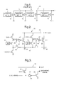
- FIG. 1 A structure to effect such a connection is shown in FIG. 1. Specifically, in FIG. 1 there is shown a structure (generally designated by reference numeral 10) for connecting an bus having "n" lines to a bus having only one line.
- the individual lines of the n line bus shown in FIG. 1 are designated X0, X1, X2... Xn-1.
- the line bus shown in FIG. 1 is simply designated Y.
- the structure 10 comprises n transistors (each designated by reference numeral 12), one each for each line of the n line bus.
- n transistors each designated by reference numeral 12
- a single bit of data effectively controls each of the n transistors 12.
- These bits are depicted in FIG. 1 in the form of memory bit boxes (each designated by reference numeral 14), each of which is connected to the gate of an associated transistor 12.
- Each of the bits in the "memory cells" 14 may be enabled, therefore allowing connection of the associated X and the Y line (e.g., enabling memory bit 0 allows connection of line XO and the Y line) and transmission of data on the relevant X line to the Y line (e.g., XO to Y in the example being presented).
- FIG. 1 has certain shortcomings, however. It is possible, for example, if any two of the memory cells are on and if they differ, line Y can be in an unknown state. More specifically, as an example, XO and X1 could differ. If, in such a case, both memory bits 0 and 1 were enabled, the value on line Y would be unknown. Further, there would exist a high current path between lines XO and X1 in such a case, assuming that both transistors TO and T1 were enabled and that the transistors were of relatively large values for speed.
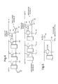
- FIG. 2 there is shown a schematic diagram of a circuit (generally designated by reference numeral 16) according to the teachings of the present invention.
- Circuit 16 may be seen in FIG. 2 to comprise a plurality of memory cell bits 18, two of which are shown in FIG. 2.
- memory cell bits 18 are EE memory cell bits.
- Memory call bits 18 could, for example, be EPROM bits or flash cell structures or even simply static RAM cells.
- memory cell bits 18 may be programmed “on” or “off”. If, for example, the left-most memory cell bit 18 in FIG. 2 were programmed "on”, Node A (designated by reference numeral 20) will be pulled low. Node A 20 being pulled low will, in turn, cause inverter 22 to go high, also pulling pass gate 1 ("P1 ") (designated by reference numeral 24) high. Pass gate 1 24 going high connects line XO 26 to line YOUT 28.
- P1 pass gate 1
- the ground line pass gate 30 when Node A 20 is low, the ground line pass gate 30 will also be low, eliminating the ground path 32 to the right-most portion of the circuit (the second "cell") shown in FIG. 2. Eliminating the ground path 32 causes Node B 34 to go high regardless of the programmed state of its associated memory cell bit (i.e., the right-most memory cell bit 18 depicted in FIG. 2).
- inverter 2 36 pulls pass gate 2 ("P2") 38 low. With pass gate 2 38 low, connection of line X1 40 and line YOUT 28 is not possible. Therefore, in operation of the circuit depicted in FIG. 2, there is no possibility that multiple cells will be selected on YOUT.
- bus lines x0 and x1 are shown in FIG. 2, those skilled in the art will readily appreciate that any number of such lines, with associated stage elements (i.e., memory cell bits, inverters, etc. ), could be connected to form an embodiment of the present invention.
- stage elements i.e., memory cell bits, inverters, etc.
- the only real limit on the number of "cells” or “stages” that could be so “stacked” is a requirement that the ground path 32 offer low enough resistance that each subsequent cell is pulled low, enabling the associated pass gates.
- Circuit 42 comprises a biasing mechanism (generally designated by reference numeral 44), an inverter 46, and a pass gate 48 which interact to effectively amplify the grounding signal and thereby allow a greater number of cells or stages to be stacked.
- the present invention provides an ordered method for considering whether to connect each one of a plurality of wide bus lines to a single bus line.
- the method of the present invention includes the step of disabling all possible subsequent connections once a connection is made. This latter step allows a very wide multiplexer to be created in which it is certain that multi-selection will not occur.
- the present invention provides an improved multiplexer system wherein a plurality of wide bus lines may be connected to a single bus line and wherein each of the plurality of wide bus lines is routed through an individual pass gate before connection to the single bus line.
- an improved system includes structure for imposing ordered consideration of each of the plurality of wide bus lines to determine whether it should be connected to the single bus line, structure for enabling connection of a first one of the plurality of wide bus lines to the single bus line, and structure for disabling possible connection of each of the plurality of wide bus lines subsequent to the first one of the plurality of wide bus lines.
- the apparatus of the present invention is very simple, and thus less expensive to make and more compact than more elaborate systems that could be constructed to perform the same function.
- the method of the present invention, employing grounding signal expansion also can be advantageously employed because it is not binary and because any width, or number of input signals, is possible.
- Such buffering could be provided by a circuit scheme such as that depicted in FIG. 4.
- This buffering circuit scheme comprises multiple stages terminating with a biasing mechanism 48, a tristate buffer 50, an inverter 52, and a grounding signal pass gate 54.
- FIG. 4 shows two such stages, both referenced identically. It such be appreciated, however, that any number of such stages could be included in an embodiment of the present invention, although the larger the number of such stages, the slower overall circuit performance would be.
- the absolute final stage would not require a tristate buffer or a final grounding amplifier. It would still be necessary, though, to make the final stage deselect (that is, pull high or low). This could be effected by the circuit scheme depicted in FIG. 5, which circuit scheme employs a buffer 56 and pass gate 58 disposed in the out line and the grounding line, respectively, as shown.
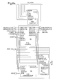
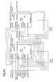
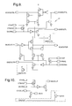
- FIGs 6-10 are included herewith to illustrate particular embodiments of the present invention that have heretofore been constructed and tested and been shown to operate very well.
- the circuits shown in FIGs 6-10 are presented here as examples only and are not, and should not in any way be construed to be, limiting as to details of practice of the present invention.
- FIG 6 depicts, in the form of a detailed circuit diagram, an apparatus according to the teachings of the present invention.
- the apparatus of FIG 6 is really quite simple and constructed of very few parts: two MUXOUT elements 60; virtually identical MUXROW and MUXROWR elements 62, 64; two INTMATENDCAP elements 66; two ROWPUMP elements 68; and an INTMAT-BUF element 70.
- FIG 7 depicts an even more detailed view of MUXROW element 62, which is shown therein to essentially comprise a BITXL element 72 and a BITXR element 74.
- MUXROW element 62 depicted in detail in FIG. 7, is virtually identical to MUXROWR element 64, depicted in FIG 6.
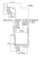
- FIG. 8 there is shown a detailed circuit diagram of the BITXR element 74, a higher level view of which is presented in FIG. 7.
- a transistor 78 that forms essentially the only difference between the BITXR element 74 and the BITXL element 72.
- FIG. 9 there is shown a detailed circuit diagram of a grounding signal amplifier 42, a higher level view of which is presented in FIG. 3.
- FIG. 10 depicts buffering and buffering termination schemes, shown and discussed previously in FIGs 4 and 5 and in the description accompanying those FIGs.
- the present invention broadly speaking, provides a method and apparatus for connecting a wide line bus to a single line bus, wherein the connecting of one of the wide bus lines triggers means for disabling possible connection of all other wide bus lines. Performing in this manner, the present invention allows a very wide multiplexer to be created, in which multiplexer it is certain that multi-selection of wide bus lines will not occur.
Landscapes
- Electronic Switches (AREA)
Applications Claiming Priority (2)
| Application Number | Priority Date | Filing Date | Title |
|---|---|---|---|
| US24521 | 1993-03-01 | ||
| US08/024,521 US5307352A (en) | 1993-03-01 | 1993-03-01 | Switch matrix multiplexers |
Publications (3)
| Publication Number | Publication Date |
|---|---|
| EP0614293A2 true EP0614293A2 (fr) | 1994-09-07 |
| EP0614293A3 EP0614293A3 (fr) | 1997-03-05 |
| EP0614293B1 EP0614293B1 (fr) | 2002-12-18 |
Family
ID=21821020
Family Applications (1)
| Application Number | Title | Priority Date | Filing Date |
|---|---|---|---|
| EP94300558A Expired - Lifetime EP0614293B1 (fr) | 1993-03-01 | 1994-01-26 | Multiplexeur |
Country Status (4)
| Country | Link |
|---|---|
| US (1) | US5307352A (fr) |
| EP (1) | EP0614293B1 (fr) |
| JP (1) | JP3644982B2 (fr) |
| DE (1) | DE69431892T2 (fr) |
Families Citing this family (2)
| Publication number | Priority date | Publication date | Assignee | Title |
|---|---|---|---|---|
| US6563730B1 (en) | 2002-04-09 | 2003-05-13 | National Semiconductor Corporation | Low power static RAM architecture |
| US6711051B1 (en) | 2002-09-05 | 2004-03-23 | National Semiconductor Corporation | Static RAM architecture with bit line partitioning |
Family Cites Families (9)
| Publication number | Priority date | Publication date | Assignee | Title |
|---|---|---|---|---|
| US4390988A (en) * | 1981-07-14 | 1983-06-28 | Rockwell International Corporation | Efficient means for implementing many-to-one multiplexing logic in CMOS/SOS |
| JPS58184822A (ja) * | 1982-03-31 | 1983-10-28 | Fujitsu Ltd | 入力回路 |
| JPS6030215A (ja) * | 1983-07-28 | 1985-02-15 | Toshiba Corp | Cmos論理回路 |
| JPS61263313A (ja) * | 1985-05-17 | 1986-11-21 | Matsushita Electric Ind Co Ltd | セレクタ付ラツチ回路 |
| JPS62165788A (ja) * | 1986-01-16 | 1987-07-22 | Sharp Corp | 半導体集積回路装置 |
| US4868413A (en) * | 1988-04-20 | 1989-09-19 | International Business Machines Corporation | Testable passgate logic circuits |
| US5001367A (en) * | 1989-04-14 | 1991-03-19 | Thunderbird Technologies, Inc. | High speed complementary field effect transistor logic circuits |
| JPH0834395B2 (ja) * | 1989-10-11 | 1996-03-29 | 株式会社東芝 | スイッチ付き増幅回路 |
| US5086427A (en) * | 1990-04-09 | 1992-02-04 | Unisys Corporation | Clocked logic circuitry preventing double driving on shared data bus |
-
1993
- 1993-03-01 US US08/024,521 patent/US5307352A/en not_active Expired - Lifetime
-
1994
- 1994-01-26 DE DE69431892T patent/DE69431892T2/de not_active Expired - Fee Related
- 1994-01-26 EP EP94300558A patent/EP0614293B1/fr not_active Expired - Lifetime
- 1994-02-28 JP JP02972294A patent/JP3644982B2/ja not_active Expired - Fee Related
Also Published As
| Publication number | Publication date |
|---|---|
| DE69431892D1 (de) | 2003-01-30 |
| JPH06324775A (ja) | 1994-11-25 |
| DE69431892T2 (de) | 2003-11-13 |
| EP0614293B1 (fr) | 2002-12-18 |
| JP3644982B2 (ja) | 2005-05-11 |
| US5307352A (en) | 1994-04-26 |
| EP0614293A3 (fr) | 1997-03-05 |
Similar Documents
| Publication | Publication Date | Title |
|---|---|---|
| JP2717111B2 (ja) | 送信ゲート直列マルチプレクサ | |
| US5396108A (en) | Latch controlled output driver | |
| NL8900795A (nl) | Informatie-uitgangsbufferschakeling voor byte-breed geheugen. | |
| EP0332077A3 (fr) | Circuit intégré semi-conducteur employant des transistors bipolaires et CMOS | |
| JPH0344890A (ja) | 半導体記憶装置のデータ出力制御回路 | |
| US5012126A (en) | High speed CMOS multiplexer having reduced propagation delay | |
| EP0235889B1 (fr) | Circuit de lecture des données pour un dispositif de mémoire à semi-conducteur | |
| US5982220A (en) | High speed multiplexer circuit | |
| US5307352A (en) | Switch matrix multiplexers | |
| US5515024A (en) | High performance dynamic compare circuit | |
| US5834949A (en) | Bus driver failure detection system | |
| US4885544A (en) | Determination circuit for data coincidence | |
| EP0096896A2 (fr) | Circuit de transmission pour signaux | |
| US6366520B1 (en) | Method and system for controlling the slew rate of signals generated by open drain driver circuits | |
| KR100400113B1 (ko) | 고성능의다이나믹비교회로및감지증폭기공통모드딥필터회로 | |
| US4931667A (en) | Circuit arrangement for a dual bus line | |
| US4808857A (en) | Sense amplifier circuit for switching plural inputs at low power | |
| US6172900B1 (en) | Compact, low voltage, noise-immune RAM cell | |
| EP0264933A2 (fr) | Système avec rétrocouplage négatif pour réduire le temps de réponse d'une cellule de mémoire | |
| US6154397A (en) | Semiconductor memory device having stabilization circuit for stable signal transmission | |
| JPH09261021A (ja) | 信号遷移検出回路 | |
| KR940008720B1 (ko) | 반도체메모리장치 | |
| US5691653A (en) | Product term based programmable logic array devices with reduced control memory requirements | |
| US5557581A (en) | Logic and memory circuit with reduced input-to-output signal propagation delay | |
| CN1204681C (zh) | 单端点感知放大器 |
Legal Events
| Date | Code | Title | Description |
|---|---|---|---|
| PUAI | Public reference made under article 153(3) epc to a published international application that has entered the european phase |
Free format text: ORIGINAL CODE: 0009012 |
|
| AK | Designated contracting states |
Kind code of ref document: A2 Designated state(s): BE DE DK ES FR GB GR IE IT LU NL PT SE |
|
| PUAL | Search report despatched |
Free format text: ORIGINAL CODE: 0009013 |
|
| AK | Designated contracting states |
Kind code of ref document: A3 Designated state(s): BE DE DK ES FR GB GR IE IT LU NL PT SE |
|
| 17P | Request for examination filed |
Effective date: 19970808 |
|
| 17Q | First examination report despatched |
Effective date: 20000731 |
|
| GRAG | Despatch of communication of intention to grant |
Free format text: ORIGINAL CODE: EPIDOS AGRA |
|
| RAP1 | Party data changed (applicant data changed or rights of an application transferred) |
Owner name: VANTIS CORPORATION |
|
| GRAG | Despatch of communication of intention to grant |
Free format text: ORIGINAL CODE: EPIDOS AGRA |
|
| GRAH | Despatch of communication of intention to grant a patent |
Free format text: ORIGINAL CODE: EPIDOS IGRA |
|
| RAP1 | Party data changed (applicant data changed or rights of an application transferred) |
Owner name: LATTICE SEMICONDUCTOR CORPORATION |
|
| GRAH | Despatch of communication of intention to grant a patent |
Free format text: ORIGINAL CODE: EPIDOS IGRA |
|
| GRAA | (expected) grant |
Free format text: ORIGINAL CODE: 0009210 |
|
| AK | Designated contracting states |
Kind code of ref document: B1 Designated state(s): BE DE DK ES FR GB GR IE IT LU NL PT SE |
|
| PG25 | Lapsed in a contracting state [announced via postgrant information from national office to epo] |
Ref country code: NL Free format text: LAPSE BECAUSE OF FAILURE TO SUBMIT A TRANSLATION OF THE DESCRIPTION OR TO PAY THE FEE WITHIN THE PRESCRIBED TIME-LIMIT Effective date: 20021218 Ref country code: IT Free format text: LAPSE BECAUSE OF FAILURE TO SUBMIT A TRANSLATION OF THE DESCRIPTION OR TO PAY THE FEE WITHIN THE PRESCRIBED TIME-LIMIT;WARNING: LAPSES OF ITALIAN PATENTS WITH EFFECTIVE DATE BEFORE 2007 MAY HAVE OCCURRED AT ANY TIME BEFORE 2007. THE CORRECT EFFECTIVE DATE MAY BE DIFFERENT FROM THE ONE RECORDED. Effective date: 20021218 Ref country code: GR Free format text: LAPSE BECAUSE OF FAILURE TO SUBMIT A TRANSLATION OF THE DESCRIPTION OR TO PAY THE FEE WITHIN THE PRESCRIBED TIME-LIMIT Effective date: 20021218 Ref country code: FR Free format text: LAPSE BECAUSE OF FAILURE TO SUBMIT A TRANSLATION OF THE DESCRIPTION OR TO PAY THE FEE WITHIN THE PRESCRIBED TIME-LIMIT Effective date: 20021218 Ref country code: BE Free format text: LAPSE BECAUSE OF FAILURE TO SUBMIT A TRANSLATION OF THE DESCRIPTION OR TO PAY THE FEE WITHIN THE PRESCRIBED TIME-LIMIT Effective date: 20021218 |
|
| REG | Reference to a national code |
Ref country code: GB Ref legal event code: FG4D |
|
| PGFP | Annual fee paid to national office [announced via postgrant information from national office to epo] |
Ref country code: SE Payment date: 20030107 Year of fee payment: 10 |
|
| PGFP | Annual fee paid to national office [announced via postgrant information from national office to epo] |
Ref country code: FR Payment date: 20030110 Year of fee payment: 10 |
|
| PGFP | Annual fee paid to national office [announced via postgrant information from national office to epo] |
Ref country code: IE Payment date: 20030117 Year of fee payment: 10 Ref country code: DK Payment date: 20030117 Year of fee payment: 10 |
|
| REG | Reference to a national code |
Ref country code: IE Ref legal event code: FG4D |
|
| PG25 | Lapsed in a contracting state [announced via postgrant information from national office to epo] |
Ref country code: LU Free format text: LAPSE BECAUSE OF NON-PAYMENT OF DUE FEES Effective date: 20030126 |
|
| PGFP | Annual fee paid to national office [announced via postgrant information from national office to epo] |
Ref country code: NL Payment date: 20030130 Year of fee payment: 10 Ref country code: GR Payment date: 20030130 Year of fee payment: 10 |
|
| REF | Corresponds to: |
Ref document number: 69431892 Country of ref document: DE Kind code of ref document: P Date of ref document: 20030130 |
|
| PGFP | Annual fee paid to national office [announced via postgrant information from national office to epo] |
Ref country code: ES Payment date: 20030218 Year of fee payment: 10 |
|
| PGFP | Annual fee paid to national office [announced via postgrant information from national office to epo] |
Ref country code: BE Payment date: 20030311 Year of fee payment: 10 |
|
| PG25 | Lapsed in a contracting state [announced via postgrant information from national office to epo] |
Ref country code: SE Free format text: LAPSE BECAUSE OF FAILURE TO SUBMIT A TRANSLATION OF THE DESCRIPTION OR TO PAY THE FEE WITHIN THE PRESCRIBED TIME-LIMIT Effective date: 20030318 Ref country code: PT Free format text: LAPSE BECAUSE OF FAILURE TO SUBMIT A TRANSLATION OF THE DESCRIPTION OR TO PAY THE FEE WITHIN THE PRESCRIBED TIME-LIMIT Effective date: 20030318 Ref country code: DK Free format text: LAPSE BECAUSE OF FAILURE TO SUBMIT A TRANSLATION OF THE DESCRIPTION OR TO PAY THE FEE WITHIN THE PRESCRIBED TIME-LIMIT Effective date: 20030318 |
|
| PG25 | Lapsed in a contracting state [announced via postgrant information from national office to epo] |
Ref country code: ES Free format text: LAPSE BECAUSE OF FAILURE TO SUBMIT A TRANSLATION OF THE DESCRIPTION OR TO PAY THE FEE WITHIN THE PRESCRIBED TIME-LIMIT Effective date: 20030627 |
|
| PLBE | No opposition filed within time limit |
Free format text: ORIGINAL CODE: 0009261 |
|
| STAA | Information on the status of an ep patent application or granted ep patent |
Free format text: STATUS: NO OPPOSITION FILED WITHIN TIME LIMIT |
|
| EN | Fr: translation not filed | ||
| 26N | No opposition filed |
Effective date: 20030919 |
|
| PG25 | Lapsed in a contracting state [announced via postgrant information from national office to epo] |
Ref country code: IE Free format text: LAPSE BECAUSE OF NON-PAYMENT OF DUE FEES Effective date: 20040126 |
|
| REG | Reference to a national code |
Ref country code: IE Ref legal event code: MM4A |
|
| PGFP | Annual fee paid to national office [announced via postgrant information from national office to epo] |
Ref country code: DE Payment date: 20070118 Year of fee payment: 14 |
|
| PGFP | Annual fee paid to national office [announced via postgrant information from national office to epo] |
Ref country code: GB Payment date: 20070124 Year of fee payment: 14 |
|
| GBPC | Gb: european patent ceased through non-payment of renewal fee |
Effective date: 20080126 |
|
| PG25 | Lapsed in a contracting state [announced via postgrant information from national office to epo] |
Ref country code: DE Free format text: LAPSE BECAUSE OF NON-PAYMENT OF DUE FEES Effective date: 20080801 |
|
| PG25 | Lapsed in a contracting state [announced via postgrant information from national office to epo] |
Ref country code: GB Free format text: LAPSE BECAUSE OF NON-PAYMENT OF DUE FEES Effective date: 20080126 |