EP0614329A1 - Verfahren zur Abdichtung eines Gehäuses, insbesondere für mikroelektronische Schaltungen, und so abgedichtetes Gehäuse - Google Patents
Verfahren zur Abdichtung eines Gehäuses, insbesondere für mikroelektronische Schaltungen, und so abgedichtetes Gehäuse Download PDFInfo
- Publication number
- EP0614329A1 EP0614329A1 EP94400468A EP94400468A EP0614329A1 EP 0614329 A1 EP0614329 A1 EP 0614329A1 EP 94400468 A EP94400468 A EP 94400468A EP 94400468 A EP94400468 A EP 94400468A EP 0614329 A1 EP0614329 A1 EP 0614329A1
- Authority
- EP
- European Patent Office
- Prior art keywords
- cover
- housing
- welding
- enclosure
- sealing
- Prior art date
- Legal status (The legal status is an assumption and is not a legal conclusion. Google has not performed a legal analysis and makes no representation as to the accuracy of the status listed.)
- Withdrawn
Links
Images

Classifications
-
- B—PERFORMING OPERATIONS; TRANSPORTING
- B23—MACHINE TOOLS; METAL-WORKING NOT OTHERWISE PROVIDED FOR
- B23K—SOLDERING OR UNSOLDERING; WELDING; CLADDING OR PLATING BY SOLDERING OR WELDING; CUTTING BY APPLYING HEAT LOCALLY, e.g. FLAME CUTTING; WORKING BY LASER BEAM
- B23K26/00—Working by laser beam, e.g. welding, cutting or boring
- B23K26/20—Bonding
- B23K26/21—Bonding by welding
- B23K26/24—Seam welding
-
- H—ELECTRICITY
- H05—ELECTRIC TECHNIQUES NOT OTHERWISE PROVIDED FOR
- H05K—PRINTED CIRCUITS; CASINGS OR CONSTRUCTIONAL DETAILS OF ELECTRIC APPARATUS; MANUFACTURE OF ASSEMBLAGES OF ELECTRICAL COMPONENTS
- H05K5/00—Casings, cabinets or drawers for electric apparatus
- H05K5/0091—Housing specially adapted for small components
- H05K5/0095—Housing specially adapted for small components hermetically-sealed
-
- H—ELECTRICITY
- H10—SEMICONDUCTOR DEVICES; ELECTRIC SOLID-STATE DEVICES NOT OTHERWISE PROVIDED FOR
- H10W—GENERIC PACKAGES, INTERCONNECTIONS, CONNECTORS OR OTHER CONSTRUCTIONAL DETAILS OF DEVICES COVERED BY CLASS H10
- H10W76/00—Containers; Fillings or auxiliary members therefor; Seals
- H10W76/60—Seals
-
- H—ELECTRICITY
- H10—SEMICONDUCTOR DEVICES; ELECTRIC SOLID-STATE DEVICES NOT OTHERWISE PROVIDED FOR
- H10W—GENERIC PACKAGES, INTERCONNECTIONS, CONNECTORS OR OTHER CONSTRUCTIONAL DETAILS OF DEVICES COVERED BY CLASS H10
- H10W95/00—Packaging processes not covered by the other groups of this subclass
Definitions
- the present invention relates to a method of hermetically closing an enclosure, in particular an enclosure containing microelectronic circuits, and to an enclosure thus obtained.
- micrometric characteristics of devices with components and connection circuits used in microelectronic technology require the packaging of these devices in enclosures in a neutral atmosphere to avoid any risk of corrosion initiation or short circuit, the development of which would be harmful to the operation of these devices. , given the very small dimensions of their components, their connecting tracks, etc.
- the airtightness of these enclosures must be of a very high level (leaks less than 1.10 ⁇ 2 Pa.cm3 / s).
- the enclosure is produced from a housing machined from a metal block in Kovar or Titanium. These materials have thermal expansion coefficients adapted to that of the substrates of microelectronic circuits.
- a cover is produced separately with the same material, and it is glued all around its periphery to the housing.
- a second type of closure starts from the same elements as those mentioned above.
- the cover is fixed to the housing by screws, ensuring the mechanical holding function.
- a groove is previously formed in the face of the housing which will be in contact with the cover, and it is filled with a silicone clogging product.
- a third type of closure which consists in welding the cover to the housing by laser beam, makes it possible to reduce the thickness of the wall of the housing.
- the laser welding must simultaneously secure the cover and seal the enclosure.
- the pressure changes due to variations in altitude strongly solder the lid, which can lead to losses of hermeticity after several cycles of pressure variations.
- welding by laser beam along the closure perimeter and on the internal partitions produces significant deformation of the casing in the form of warping (of the order of 1 to 2 mm for a casing the largest dimension of which is approximately 200 mm).
- warping is a very significant drawback when the enclosures are used in cooling structures with thermal slides which tolerate only a few tenths of a millimeter of warping.
- the subject of the present invention is a method of hermetically closing an enclosure, in particular an enclosure containing microelectronic equipment, making it possible to use an enclosure whose walls are as thin as possible and guaranteeing good mechanical strength as a function of constraints. mechanical and thermal, as well as good hermeticity, this device being easy to implement and as inexpensive as possible.
- the present invention also relates to an enclosure thus obtained.
- the closing process in accordance with the invention for a hermetic metal enclosure, of the type comprising a housing one side of which is open, and a cover closing this side, consists in producing, around the entire periphery of the cover, welded lines by laser and to seal the joint between the cover and the housing.
- the side wall of the housing is thinned before welding over its entire outer periphery near the face which will be in contact with the cover, and the throat is filled with sealing product, after welding. thus formed.
- slots are formed in the cover, before welding, along the welding line. which are then practiced the welding lines, and after welding the slots are filled with a sealing product.
- the enclosure according to the invention comprises a one-piece housing body on which a cover is welded by welded lines, and a sealing product ensuring the hermeticity of the closure.
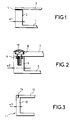
- the housing 1 essentially comprises a bottom 1 and a peripheral wall 2.
- This housing has for example a shape of a rectangular parallelepiped without its upper face.
- the bottom 1 and the wall 2 are machined, for example by milling, from a metal block (Kovar, Titanium, ).
- FIG. 2 shows another embodiment of the enclosure according to the prior art.
- the box similar to the box of FIG. 1, and machined in a similar way, comprises a bottom 5 and a peripheral wall 6.
- This wall 6 is a little thicker (thickness e2 of at least 4 mm) than the wall 2, to allow the fixing of the cover 7 using screws 8.
- a groove 9 is formed on the upper face of the wall 6 and is filled with a silicone sealing product. Clogging product 10 is also deposited on the heads of the screws 8.
- a housing 11 is machined whose walls 12 are thinner (thickness e3 of about 1.6 mm) than those of the previous embodiments, and the cover 13 over its entire periphery by welding 14 with a laser beam.
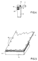
- the lateral wall 15 is thinned outwardly at its upper part, around its entire periphery.
- the thickness of the wall 15 is for example about 1.6 to 2 mm, and the thickness of its thinned upper part 16 is for example about 0.8 to 1 mm.
- the cover 17 is welded to the wall part 16 by welded lines 18 with a laser beam. These lines, regularly distributed along the welding path, for example have a length of 3 mm and are spaced from 25 to 30 mm. This minimizes the length of the welded parts, which prevents twisting of the housing.
- the sealing is then carried out by placing a polymerizable sealing product 19 in the groove 20 formed by the thinning of the upper part of the side wall.
- This clogging product is for example a silicone-based product.
- the side wall 21 of the housing is not thinned, but slots 22 are made in the cover 23, along the welding path. These slots 22 have for example a length of about 25 to 30 mm and are spaced about 3 mm apart. Their width is, of course, less than the thickness of the wall 21.
- Laser welds 24 are made between the slots, which means that the weld lines have the same length and spacing as in the case of FIGS. 4 and 5. Then a sealing product 25 is placed in the slots 22, being understood that the weld lines 24 extend to the edge of the slots which are respectively adjacent to them, and that these weld lines ensure airtightness over their entire length.
- the tank 26 containing the liquid plugging product 27 is placed in a vacuum chamber 28, and the casing (s) 29 are placed upside down in the tank 26.
- This step has for example a duration of approximately 30 minutes.
- a slight overpressure is applied (for example, a few tens of m Bar for a few tens of minutes) in the bell 28 to facilitate penetration of the clogging product into the bottom of the grooves 20 in the possible interstices between the cover 17 and the wall 16, or at the bottom of the slots 22 in the possible interstices between the cover 23 and the wall 21, without however penetrating inside the case.
- the cover can be welded to these partitions by laser welding lines having the same dimensions and spacing as the welding lines 18 of the embodiment of FIGS. 4 and 5.
Landscapes
- Engineering & Computer Science (AREA)
- Microelectronics & Electronic Packaging (AREA)
- Physics & Mathematics (AREA)
- Optics & Photonics (AREA)
- Plasma & Fusion (AREA)
- Mechanical Engineering (AREA)
- Casings For Electric Apparatus (AREA)
- Laser Beam Processing (AREA)
Applications Claiming Priority (2)
| Application Number | Priority Date | Filing Date | Title |
|---|---|---|---|
| FR9302588 | 1993-03-05 | ||
| FR9302588A FR2702329B1 (fr) | 1993-03-05 | 1993-03-05 | Procédé de fermeture hermétique d'enceinte en particulier d'enceinte contenant des circuits microélectroniques, et enceinte ainsi obtenue. |
Publications (1)
| Publication Number | Publication Date |
|---|---|
| EP0614329A1 true EP0614329A1 (de) | 1994-09-07 |
Family
ID=9444703
Family Applications (1)
| Application Number | Title | Priority Date | Filing Date |
|---|---|---|---|
| EP94400468A Withdrawn EP0614329A1 (de) | 1993-03-05 | 1994-03-04 | Verfahren zur Abdichtung eines Gehäuses, insbesondere für mikroelektronische Schaltungen, und so abgedichtetes Gehäuse |
Country Status (2)
| Country | Link |
|---|---|
| EP (1) | EP0614329A1 (de) |
| FR (1) | FR2702329B1 (de) |
Cited By (4)
| Publication number | Priority date | Publication date | Assignee | Title |
|---|---|---|---|---|
| EP1972407A1 (de) * | 2007-03-22 | 2008-09-24 | Karosseriewerke Dresden GmbH | Verfahren zur Herstellung durch Laser- oder Elektronstrahlschweissen eines Verbundkörpers ; Lehnen- und/oder Sitzstruktur |
| US8335050B2 (en) | 2007-04-03 | 2012-12-18 | Hitachi Global Storage Technologies, Netherlands B.V. | Disk drive with a solder preform hermetic seal |
| WO2013144693A3 (en) * | 2012-03-29 | 2013-12-05 | Gigaphoton Inc. | Laser apparatus and its manufacturing method, comprising frames joined together|with a bolt-based system |
| CN110961783A (zh) * | 2018-09-28 | 2020-04-07 | 大族激光科技产业集团股份有限公司 | 超薄不锈钢壳体的密封方法 |
Citations (3)
| Publication number | Priority date | Publication date | Assignee | Title |
|---|---|---|---|---|
| JPS6035540A (ja) * | 1983-08-08 | 1985-02-23 | Hitachi Ltd | 半導体装置 |
| US4521668A (en) * | 1983-11-08 | 1985-06-04 | Westinghouse Electric Corp. | Method of hermetically laser sealing electronic packages |
| JPS62261157A (ja) * | 1986-05-07 | 1987-11-13 | Nec Corp | 半導体装置用パツケ−ジ |
-
1993
- 1993-03-05 FR FR9302588A patent/FR2702329B1/fr not_active Expired - Fee Related
-
1994
- 1994-03-04 EP EP94400468A patent/EP0614329A1/de not_active Withdrawn
Patent Citations (3)
| Publication number | Priority date | Publication date | Assignee | Title |
|---|---|---|---|---|
| JPS6035540A (ja) * | 1983-08-08 | 1985-02-23 | Hitachi Ltd | 半導体装置 |
| US4521668A (en) * | 1983-11-08 | 1985-06-04 | Westinghouse Electric Corp. | Method of hermetically laser sealing electronic packages |
| JPS62261157A (ja) * | 1986-05-07 | 1987-11-13 | Nec Corp | 半導体装置用パツケ−ジ |
Non-Patent Citations (2)
| Title |
|---|
| PATENT ABSTRACTS OF JAPAN vol. 12, no. 135 (E - 604)<2982> 23 April 1988 (1988-04-23) * |
| PATENT ABSTRACTS OF JAPAN vol. 9, no. 154 (E - 325)<1877> 28 June 1985 (1985-06-28) * |
Cited By (6)
| Publication number | Priority date | Publication date | Assignee | Title |
|---|---|---|---|---|
| EP1972407A1 (de) * | 2007-03-22 | 2008-09-24 | Karosseriewerke Dresden GmbH | Verfahren zur Herstellung durch Laser- oder Elektronstrahlschweissen eines Verbundkörpers ; Lehnen- und/oder Sitzstruktur |
| US8335050B2 (en) | 2007-04-03 | 2012-12-18 | Hitachi Global Storage Technologies, Netherlands B.V. | Disk drive with a solder preform hermetic seal |
| US9412420B2 (en) | 2007-04-03 | 2016-08-09 | HGST Netherlands B.V. | Hermetically sealing a disk drive assembly |
| WO2013144693A3 (en) * | 2012-03-29 | 2013-12-05 | Gigaphoton Inc. | Laser apparatus and its manufacturing method, comprising frames joined together|with a bolt-based system |
| US9837779B2 (en) | 2012-03-29 | 2017-12-05 | Gigaphoton Inc. | Laser apparatus and laser apparatus manufacturing method |
| CN110961783A (zh) * | 2018-09-28 | 2020-04-07 | 大族激光科技产业集团股份有限公司 | 超薄不锈钢壳体的密封方法 |
Also Published As
| Publication number | Publication date |
|---|---|
| FR2702329B1 (fr) | 1995-04-07 |
| FR2702329A1 (fr) | 1994-09-09 |
Similar Documents
| Publication | Publication Date | Title |
|---|---|---|
| US6416831B1 (en) | Evacuated package and a method of producing the same | |
| EP2952471B1 (de) | Verkapselungsstruktur mit mehreren hohlräumen versehen mit zugangskanälen unterschiedlicher höhe | |
| CN101322242B (zh) | 气密密封用盖、电子器件收纳用封装体和气密密封用盖的制造方法 | |
| EP1093159A1 (de) | Verfahren zum Einkapseln von elektronischen Komponenten | |
| WO1999067818A1 (fr) | Dispositif et procede de formation d'un dispositif presentant une cavite a atmosphere controlee | |
| EP1041625A1 (de) | Elektrisches oder elektronisches Bauelement in einer versiegelten Verpackung und dessen Herstellungsverfahren | |
| EP3157050B1 (de) | Herstellungsverfahren einer mikroelektronischen vorrichtung und dadurch hergestellte mikroelektronische vorrichtung | |
| EP2507825B1 (de) | Verfahren zur montage und abdichtung eines gehäuses | |
| EP0629112B1 (de) | Hermetischer Schnellverschluss für einen Behälter | |
| EP0044755B1 (de) | Gegen hohe auswendige Drucke widerstandsfähiges Verkapselungsgehäuse für hybride Schaltung | |
| EP0614329A1 (de) | Verfahren zur Abdichtung eines Gehäuses, insbesondere für mikroelektronische Schaltungen, und so abgedichtetes Gehäuse | |
| EP3157057B1 (de) | Gehäuse für mikroelektronische bauteile | |
| CA2280937C (fr) | Boitier electronique ou optoelectronique a insert ceramique | |
| FR2466937A1 (fr) | Boitier de circuit electronique hybride | |
| FR2747005A1 (fr) | Boitier de micro-electronique avec systeme de refroidissement | |
| EP0531197B1 (de) | Verfahren zur Laserverpackung von elektronischen Schaltungen, insbesondere für Hybrid-Schaltungen zur Minimisierung von Spannungen | |
| EP1192592A1 (de) | Vorrichtung und hestellungsverfahren von vorrichtungen mit zumindest einer ic au | |
| WO2015071835A1 (fr) | Dispositif de traversée notamment pour système d'implant médical et procède de réalisation | |
| JP4089609B2 (ja) | 電子素子パッケージおよび電子素子パッケージの製造方法 | |
| EP1824779B1 (de) | Vorrichtung und verfahren zur hermetischen abdichtung eines hohlraums in einem elektronischen bauteil | |
| EP2778121A1 (de) | Einkapselungsverfahren einer Mikrovorrichtung durch anodisches Bonden | |
| FR2627875A1 (fr) | Boitier assurant la protection d'informations contenues dans un circuit electronique | |
| FR3163801A1 (fr) | Procédé d’assemblage d’un boîtier, système d’assemblage et boîtier associés | |
| WO2005114721A1 (fr) | Procede et dispositif d'encapsulation, notamment pour dispositifs micromecaniques | |
| FR2519471A1 (fr) | Procede de fabrication d'une embase pour circuit integre et embase ainsi realisee |
Legal Events
| Date | Code | Title | Description |
|---|---|---|---|
| PUAI | Public reference made under article 153(3) epc to a published international application that has entered the european phase |
Free format text: ORIGINAL CODE: 0009012 |
|
| AK | Designated contracting states |
Kind code of ref document: A1 Designated state(s): DE FR GB IT |
|
| STAA | Information on the status of an ep patent application or granted ep patent |
Free format text: STATUS: THE APPLICATION IS DEEMED TO BE WITHDRAWN |
|
| 18D | Application deemed to be withdrawn |
Effective date: 19950308 |