EP0615150A2 - Substrat pour panneau d'affichage à cristal liquide - Google Patents
Substrat pour panneau d'affichage à cristal liquide Download PDFInfo
- Publication number
- EP0615150A2 EP0615150A2 EP94102567A EP94102567A EP0615150A2 EP 0615150 A2 EP0615150 A2 EP 0615150A2 EP 94102567 A EP94102567 A EP 94102567A EP 94102567 A EP94102567 A EP 94102567A EP 0615150 A2 EP0615150 A2 EP 0615150A2
- Authority
- EP
- European Patent Office
- Prior art keywords
- cover glass
- glass
- accordance
- array
- microlens
- Prior art date
- Legal status (The legal status is an assumption and is not a legal conclusion. Google has not performed a legal analysis and makes no representation as to the accuracy of the status listed.)
- Withdrawn
Links
Images


Classifications
-
- G—PHYSICS
- G02—OPTICS
- G02B—OPTICAL ELEMENTS, SYSTEMS OR APPARATUS
- G02B5/00—Optical elements other than lenses
- G02B5/18—Diffraction gratings
- G02B5/1876—Diffractive Fresnel lenses; Zone plates; Kinoforms
-
- G—PHYSICS
- G02—OPTICS
- G02B—OPTICAL ELEMENTS, SYSTEMS OR APPARATUS
- G02B3/00—Simple or compound lenses
- G02B3/0006—Arrays
- G02B3/0037—Arrays characterized by the distribution or form of lenses
- G02B3/0056—Arrays characterized by the distribution or form of lenses arranged along two different directions in a plane, e.g. honeycomb arrangement of lenses
-
- G—PHYSICS
- G02—OPTICS
- G02B—OPTICAL ELEMENTS, SYSTEMS OR APPARATUS
- G02B5/00—Optical elements other than lenses
- G02B5/18—Diffraction gratings
- G02B5/1876—Diffractive Fresnel lenses; Zone plates; Kinoforms
- G02B5/188—Plurality of such optical elements formed in or on a supporting substrate
- G02B5/1885—Arranged as a periodic array
-
- G—PHYSICS
- G02—OPTICS
- G02F—OPTICAL DEVICES OR ARRANGEMENTS FOR THE CONTROL OF LIGHT BY MODIFICATION OF THE OPTICAL PROPERTIES OF THE MEDIA OF THE ELEMENTS INVOLVED THEREIN; NON-LINEAR OPTICS; FREQUENCY-CHANGING OF LIGHT; OPTICAL LOGIC ELEMENTS; OPTICAL ANALOGUE/DIGITAL CONVERTERS
- G02F1/00—Devices or arrangements for the control of the intensity, colour, phase, polarisation or direction of light arriving from an independent light source, e.g. switching, gating or modulating; Non-linear optics
- G02F1/01—Devices or arrangements for the control of the intensity, colour, phase, polarisation or direction of light arriving from an independent light source, e.g. switching, gating or modulating; Non-linear optics for the control of the intensity, phase, polarisation or colour
- G02F1/13—Devices or arrangements for the control of the intensity, colour, phase, polarisation or direction of light arriving from an independent light source, e.g. switching, gating or modulating; Non-linear optics for the control of the intensity, phase, polarisation or colour based on liquid crystals, e.g. single liquid crystal display cells
- G02F1/133—Constructional arrangements; Operation of liquid crystal cells; Circuit arrangements
- G02F1/1333—Constructional arrangements; Manufacturing methods
- G02F1/1335—Structural association of cells with optical devices, e.g. polarisers or reflectors
- G02F1/133526—Lenses, e.g. microlenses or Fresnel lenses
-
- G—PHYSICS
- G02—OPTICS
- G02B—OPTICAL ELEMENTS, SYSTEMS OR APPARATUS
- G02B3/00—Simple or compound lenses
- G02B3/0006—Arrays
- G02B3/0012—Arrays characterised by the manufacturing method
- G02B3/0018—Reflow, i.e. characterized by the step of melting microstructures to form curved surfaces, e.g. manufacturing of moulds and surfaces for transfer etching
-
- G—PHYSICS
- G02—OPTICS
- G02B—OPTICAL ELEMENTS, SYSTEMS OR APPARATUS
- G02B3/00—Simple or compound lenses
- G02B3/0087—Simple or compound lenses with index gradient
-
- G—PHYSICS
- G02—OPTICS
- G02B—OPTICAL ELEMENTS, SYSTEMS OR APPARATUS
- G02B3/00—Simple or compound lenses
- G02B3/02—Simple or compound lenses with non-spherical faces
- G02B3/08—Simple or compound lenses with non-spherical faces with discontinuous faces, e.g. Fresnel lens
-
- G—PHYSICS
- G02—OPTICS
- G02F—OPTICAL DEVICES OR ARRANGEMENTS FOR THE CONTROL OF LIGHT BY MODIFICATION OF THE OPTICAL PROPERTIES OF THE MEDIA OF THE ELEMENTS INVOLVED THEREIN; NON-LINEAR OPTICS; FREQUENCY-CHANGING OF LIGHT; OPTICAL LOGIC ELEMENTS; OPTICAL ANALOGUE/DIGITAL CONVERTERS
- G02F1/00—Devices or arrangements for the control of the intensity, colour, phase, polarisation or direction of light arriving from an independent light source, e.g. switching, gating or modulating; Non-linear optics
- G02F1/01—Devices or arrangements for the control of the intensity, colour, phase, polarisation or direction of light arriving from an independent light source, e.g. switching, gating or modulating; Non-linear optics for the control of the intensity, phase, polarisation or colour
- G02F1/13—Devices or arrangements for the control of the intensity, colour, phase, polarisation or direction of light arriving from an independent light source, e.g. switching, gating or modulating; Non-linear optics for the control of the intensity, phase, polarisation or colour based on liquid crystals, e.g. single liquid crystal display cells
- G02F1/133—Constructional arrangements; Operation of liquid crystal cells; Circuit arrangements
- G02F1/1333—Constructional arrangements; Manufacturing methods
- G02F1/133302—Rigid substrates, e.g. inorganic substrates
Definitions
- the invention relates to a cover glass for a liquid crystal display (LCD) panel embodying an array of microlenses, of particular use in TV applications.
- LCD liquid crystal display
- Lens arrays composed of a pattern of lenses formed on a surface of a substrate, are well known.
- An early technique for forming such an array involved forming a spherical surface on one end of each of a plurality of rods. The rods were then combined as by bundling and fusion sealing.
- Microlens arrays may also be made by developing a gradient refractive index (GRIN) in a glass body through ion exchange, as in United States Patent Nos. 3,658,407 and 3,667,832, or by impregnating a porous glass body with a photolyzable, organometallic compound and then exposing the impregnated body to photolyzing light, see United states Patent No. 4,501,468.
- GRIN gradient refractive index
- Basic purposes of our invention are to produce an improved cover glass for an LCD panel that embodies a microlens array, to simplify the alignment problems heretofore encountered, and to provide an LCD TV projector having enhanced brightness.
- our invention resides in an integral cover glass for an LCD panel having an array of microlenses integral with the outside of its front face, whereby light is focused by each microlens to enhance light output from the respective pixel with which it is aligned in the panel.
- the array of microlenses is composed of either diffractive gratings or spherical-shaped surfaces.
- the cover glass is capable of being treated to form a microlens array on its outer face.
- FIGURE 1 is a schematic side view illustrating the elements in a typical LCD panel.
- FIGURE 2 is a schematic side view of the LCD panel of FIGURE 1 associated with a lens array.
- FIGURE 3 is a schematic side view of a single pixel in an LCD panel illustrating the present invention.
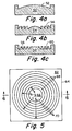
- FIGURES 4A, 4B and 4C are views in cross-section that illustrate the evolutionary development of a diffraction grating microlens for use in accordance with the invention.
- FIGURE 5 is a front view of a cover glass for a single pixel illustrating an alternative form of the invention.
- FIGURE 6 is a cross-section view along line 6-6 on FIGURE 5.
- FIGURE 7 is a view in cross-section of a fragment of FIGURE 6 showing a groove further modified.
- FIGURE 1 in the accompanying drawing is a schematic side view illustrating the elements in panel 10 for an LCD TV projector.
- Panel 10 comprises a first cover glass 12 positioned to receive light from a light source (not shown).
- Cover glass 12 typically has an electroconductive film 14 applied to its inside face 16.
- Film 14 may be a transparent conductor, for example, an indium oxide film doped with tin oxide (ITO).
- Film 14 may be continuous, or patterned.
- Panel 10 further comprises a second cover glass 18 on the inside face 20 of which is formed an x-y matrix of conducting lines. Transistors are placed at the intersections of said lines to form an array of transistors 22.
- Transistors 22 may, for example, be either amorphous silicon or polycrystalline silicon, as used in active matrix LCD devices (AMLCDs).
- AMLCDs active matrix LCD devices
- the amorphous silicon transistor requires a maximum processing temperature of 350-400°C, whereas the polycrystalline transistor requires a maximum processing temperature in the range of 600-650°C.
- liquid crystal material 24 is a liquid crystal material 24.
- suitable materials are well known and form no part of this invention.
- Transistors 22 and associated conductor lines occupy a substantial portion of the area on the face of cover glass 18. The amount is dependent on pixel size, and commonly amounts to 50-60% of the total area. Since both the transistors and the lines are essentially opaque, they necessarily limit the amount of light that can be transmitted by panel 10. It is important, then, to enhance the amount of light transmitted through the open areas to the extent possible.
- FIGURE 2 is a schematic side view showing a typical arrangement in which a lens array 26 is mounted adjacent to the front face of cover glass 12 of panel 10. The need for precise alignment of the lens array 26 with the open areas on cover glass 18 is readily apparent.
- the present invention eliminates the step of assembling the microlens array and the front cover by combining the lens array and the front cover glass of a panel into an integral body.
- the microlens array and the pixels must still be aligned, but this becomes part of the process of joining cover glasses 12 and 18 together. It avoids the separate step required in the FIGURE 2 assembly. Further, it brings the microlens array as close as possible to the pixels.
- FIGURE 3 a schematic side view of a single pixel in an LCD panel.
- the view is greatly exaggerated for illustration purposes. It will be appreciated that a typical panel may contain thousands of pixels.
- the microlens diameter may be on the order of 50-200 microns, consistent with the pixel size.
- FIGURE 3 shows a single pixel 30.
- Pixel 30 has a front cover glass 32 on the front face of which is formed one microlens 34 of a lens array.
- An electroconductive film 36 is applied, either directly to the inside face 48 of cover glass 32, or over a barrier layer 46 deposited on inside face 48.
- back cover glass 38 has transistors 40 formed thereon. This leaves open area 42 through which light may be transmitted.
- FIGURE 3 further illustrates the manner in which light is focused in accordance with the invention.
- light rays 44 are focused on open area 42 thereby enhancing the light available for open area 42.
- a microlens array may be produced on any glass having a lens forming capability. This may be a photosensitive glass as described in the Bellman et al. patents -611 and -026 mentioned earlier. Alternatively, such a microlens array may be produced by the ion exchange technique for producing a gradient refractive index in an ion exchangeable glass.
- Glasses known to have lens forming capabilities also may contain substantial quantities of alkali metal oxides.
- photosensitive glasses, as well as glasses used to form a microlens array by ion exchange may contain amounts of alkali metal oxide up to as much as 20% by weight.
- Migration of the alkali metal ions from the glass tends to occur during the heat treatment required to apply transparent electroconductive film 36.
- Typical heat treatment conditions to produce an ITO film are 300°C for one hour. The entry of such migrating alkali metal ions is detrimental to both film 36 and the liquid crystal material 24.
- a barrier layer 46 intermediate film 36 and the inside face 48 of front cover glass 32.
- This barrier layer may be chosen from transparent, colorless, refractory film materials, such as, silica, alumina, or silicon nitride. These and others are disclosed, for example, in pending application S.N. 07/853,587, filed March 18, 1992 in the name of F. P. Albertner.
- barrier films may be divided into two classes; chemical vapor deposition (CVD) and physical vapor deposition (PVD).
- CVD chemical vapor deposition
- PVD physical vapor deposition
- a barrier layer in controlling the movement of sodium out of a soda lime glass into a barrier layer of PVD silica was measured using secondary ion mass spectroscopy (SIMS).
- the barrier layers were profiled in depth. Ion counts for sodium and silicon were determined and the ratio of the two calculated.
- Such low-alkali glasses do not have the inherent capability of forming an array of microlenses.
- such glasses may be employed in the present invention by forming an array of diffraction grating microlenses on their surface. The method is to use a diffraction grating to focus the light.
- the wavefront produced by a spherical surface is expressed as, where ⁇ represents the phase as a function of the radial distance r away from the axis and f is the desired focal length of the lens at wavelength ⁇ .
- the wavelength is chosen to match the color to be transmitted by the pixel with which the lens is registered.
- FIGURE 4A a view in cross-section, illustrates an idealized microlens 50.
- This microlens would have a surface 52 adapted to produce a wavefront corresponding to the formula.
- a lens surface is impractical to produce.
- FIGURE 4B a view in cross-section, of an idealized, Fresnel-type microlens 54 having a typical Fresnel lens structure 56. Again this is impractical to produce.
- FIGURE 4C a view in cross-section, shows a microlens 58 with a single-step diffraction grating 60.
- FIGURE 4C also shows, in dashed lines, the Fresnel lens surface 56 that is collapsed to form diffraction grating 60.
- a wavelength step is chosen as one wave, or some fraction k of a wave.
- the depth of the step is k ⁇ /(n-1), where n is the refractive index of the glass.
- FIGURE 5 is a top plan view of an outer, plano face 62 on a front cover glass 64 showing a diffraction grating pattern 66 etched in plano surface 62.
- Each grating pattern 66 is composed of successive, spaced, annular surfaces 68 separated by annular elevations 70.
- Diffraction grating pattern 66 may, for example, be generated in outside plano surface 62, opposite to surface 72, which faces the liquid crystal material, by ion etching.
- pattern 66 well known photolithographic practice, as used in forming microcircuitry, is employed.
- a photoresist is first applied over plano surface 62.
- This photoresist is then covered with a grating photo mask in which the individual patterns are located to match the pixel pitch on the transistor plane of the LCD.
- the photoresist is then exposed through the photo mask to selectively develop the pattern of the mask in the photoresist layer. This exposes corresponding portions of underlying plano glass surface 62.
- the exposed portions of surface 62 are then etched, for example, by reactive ion etching to a desired depth to form annular surfaces 68. If one desires a more efficient grating, each step in the pattern is subdivided into smaller steps by additional photolithography and etching operations.
- FIGURE 7 is an enlarged, fragmented view in cross-section. It shows a single unit corresponding to a surface 68 and an adjoining elevation 70 of FIGURE 6. The unit is subdivided to form two steps, or surfaces, 74 and 76 and adjoining elevation 78, as produced by successive photolithographic and etching steps.
- the method described by Mersereau et al. contemplates applying a positive photoresist to a glass surface, exposing the photoresist-coated surface through a suitable mask and developing to provide an array of photoresist cylinders. The cylinders are then melted to form nearly spherical surfaces due to minimizing surface energy.
- the pattern is then transferred to the glass by reactive ion etching the total surface with a gas mixture balance designed to provide a 1:1 etch ratio of glass and photoresist. Once the photoresist is completely removed, the desired glass microlens array pattern remains.
- a barrier layer for alkali must be deposited on the surface of the glass which is coated with a transparent conductor. The barrier is placed between the glass surface and the transparent conducting film as described above and shown in FIGURE 3.
Landscapes
- Physics & Mathematics (AREA)
- General Physics & Mathematics (AREA)
- Optics & Photonics (AREA)
- Nonlinear Science (AREA)
- Mathematical Physics (AREA)
- Chemical & Material Sciences (AREA)
- Crystallography & Structural Chemistry (AREA)
- Liquid Crystal (AREA)
- Glass Compositions (AREA)
- Surface Treatment Of Glass (AREA)
Applications Claiming Priority (2)
| Application Number | Priority Date | Filing Date | Title |
|---|---|---|---|
| US2741293A | 1993-03-08 | 1993-03-08 | |
| US27412 | 1993-03-08 |
Publications (2)
| Publication Number | Publication Date |
|---|---|
| EP0615150A2 true EP0615150A2 (fr) | 1994-09-14 |
| EP0615150A3 EP0615150A3 (fr) | 1994-12-21 |
Family
ID=21837600
Family Applications (1)
| Application Number | Title | Priority Date | Filing Date |
|---|---|---|---|
| EP94102567A Withdrawn EP0615150A3 (fr) | 1993-03-08 | 1994-02-21 | Substrat pour panneau d'affichage à cristal liquide. |
Country Status (3)
| Country | Link |
|---|---|
| EP (1) | EP0615150A3 (fr) |
| JP (1) | JPH06294956A (fr) |
| TW (1) | TW297104B (fr) |
Cited By (10)
| Publication number | Priority date | Publication date | Assignee | Title |
|---|---|---|---|---|
| GB2318201A (en) * | 1996-10-09 | 1998-04-15 | Lg Electronics Inc | Liquid crystal displays |
| US5932342A (en) * | 1996-11-14 | 1999-08-03 | Nashua Corporation | Optical diffusers obtained by fluid phase mixing of incompatible materials |
| EP1008012A4 (fr) * | 1997-01-29 | 2000-06-14 | Corning Inc | Mosaique de lentilles sur panneau d'affichage a cristaux liquides et procede correspondant |
| US6570324B1 (en) | 2000-07-19 | 2003-05-27 | Eastman Kodak Company | Image display device with array of lens-lets |
| FR2836238A1 (fr) * | 2002-02-19 | 2003-08-22 | Kis | Procede pour transferer une image numerique en vue de sa restitution visuelle, et dispositif pour la mise en oeuvre de ce procede |
| US7241559B2 (en) | 2002-10-04 | 2007-07-10 | Corning Incorporated | Lens array and method for fabricating the lens array |
| EP1801636A4 (fr) * | 2004-09-10 | 2007-10-17 | Sumitomo Electric Industries | Ecran d'affichage translucide et procede de fabrication de celui-ci |
| EP1696248A4 (fr) * | 2003-12-19 | 2007-10-17 | Sumitomo Electric Industries | Micro-lentille de type a feuille plate et procede de production de celle-ci |
| CN104407444A (zh) * | 2014-10-17 | 2015-03-11 | 河北冀雅电子有限公司 | 一种用于液晶屏的全视角3d光栅结构 |
| DE102024128551A1 (de) * | 2024-10-02 | 2026-04-02 | Carl Zeiss Jena Gmbh | Verfahren zur Herstellung einer Anzeigevorrichtung und Anzeigevorrichtung |
Family Cites Families (5)
| Publication number | Priority date | Publication date | Assignee | Title |
|---|---|---|---|---|
| JPS5711320A (en) * | 1980-06-24 | 1982-01-21 | Sharp Corp | Liquid crystal display device |
| JPS60165621A (ja) * | 1984-02-08 | 1985-08-28 | Nec Corp | 透過型表示素子 |
| JPS60165624A (ja) * | 1984-02-08 | 1985-08-28 | Nec Corp | 透過型表示素子 |
| EP0450780A3 (en) * | 1990-04-05 | 1992-04-15 | Matsushita Electric Industrial Co., Ltd. | Optical microelement array and its production method |
| JP2849492B2 (ja) * | 1991-05-31 | 1999-01-20 | シャープ株式会社 | 投影型液晶表示装置 |
-
1994
- 1994-02-21 EP EP94102567A patent/EP0615150A3/fr not_active Withdrawn
- 1994-03-08 JP JP6036666A patent/JPH06294956A/ja not_active Withdrawn
- 1994-03-30 TW TW083102064A patent/TW297104B/zh active
Cited By (14)
| Publication number | Priority date | Publication date | Assignee | Title |
|---|---|---|---|---|
| GB2318201A (en) * | 1996-10-09 | 1998-04-15 | Lg Electronics Inc | Liquid crystal displays |
| GB2318201B (en) * | 1996-10-09 | 1999-05-05 | Lg Electronics Inc | Liquid crystal displays |
| US5932342A (en) * | 1996-11-14 | 1999-08-03 | Nashua Corporation | Optical diffusers obtained by fluid phase mixing of incompatible materials |
| EP1008012A4 (fr) * | 1997-01-29 | 2000-06-14 | Corning Inc | Mosaique de lentilles sur panneau d'affichage a cristaux liquides et procede correspondant |
| US6570324B1 (en) | 2000-07-19 | 2003-05-27 | Eastman Kodak Company | Image display device with array of lens-lets |
| WO2003071778A1 (fr) * | 2002-02-19 | 2003-08-28 | Kis | Procede pour transferer une image numerique en vue de sa restitution visuelle, et dispositif pour la mise en oeuvre de ce procede |
| FR2836238A1 (fr) * | 2002-02-19 | 2003-08-22 | Kis | Procede pour transferer une image numerique en vue de sa restitution visuelle, et dispositif pour la mise en oeuvre de ce procede |
| US6927837B2 (en) | 2002-02-19 | 2005-08-09 | Kis | Method for transferring a digital image so as to visually restore said digital image, and device for carrying out said method |
| US7241559B2 (en) | 2002-10-04 | 2007-07-10 | Corning Incorporated | Lens array and method for fabricating the lens array |
| EP1696248A4 (fr) * | 2003-12-19 | 2007-10-17 | Sumitomo Electric Industries | Micro-lentille de type a feuille plate et procede de production de celle-ci |
| EP1801636A4 (fr) * | 2004-09-10 | 2007-10-17 | Sumitomo Electric Industries | Ecran d'affichage translucide et procede de fabrication de celui-ci |
| CN104407444A (zh) * | 2014-10-17 | 2015-03-11 | 河北冀雅电子有限公司 | 一种用于液晶屏的全视角3d光栅结构 |
| CN104407444B (zh) * | 2014-10-17 | 2017-07-04 | 河北冀雅电子有限公司 | 一种用于液晶屏的全视角3d光栅结构 |
| DE102024128551A1 (de) * | 2024-10-02 | 2026-04-02 | Carl Zeiss Jena Gmbh | Verfahren zur Herstellung einer Anzeigevorrichtung und Anzeigevorrichtung |
Also Published As
| Publication number | Publication date |
|---|---|
| JPH06294956A (ja) | 1994-10-21 |
| TW297104B (fr) | 1997-02-01 |
| EP0615150A3 (fr) | 1994-12-21 |
Similar Documents
| Publication | Publication Date | Title |
|---|---|---|
| US6437918B1 (en) | Method of manufacturing flat plate microlens and flat plate microlens | |
| KR940006986B1 (ko) | 액정표시장치 | |
| EP0570176B1 (fr) | Panneau d'affichage à cristal liquide et son procédé de fabrication | |
| US5453876A (en) | Microlens array | |
| US6618200B2 (en) | System and method for providing a substrate having micro-lenses | |
| EP1801636B1 (fr) | Ecran d'affichage translucide et procede de fabrication de celui-ci | |
| CN101614920B (zh) | 一种制造液晶显示器件的方法 | |
| US20020118271A1 (en) | Exposure unit for image forming apparatus using electrophotographic system, electrophotographic image forming apparatus | |
| JP3535610B2 (ja) | 液晶プロジェクタ−用の液晶デバイスおよび液晶デバイス用の対向基板 | |
| US7052806B2 (en) | Exposure controlling photomask and production method therefor | |
| JPH06294956A (ja) | Lcdパネル用のカバーガラス | |
| US6917402B2 (en) | Opposite substrate for liquid crystal display panel with particular microlenses and layered light shields, and method of fabricating the same | |
| EP1008012B1 (fr) | Mosaique de lentilles sur panneau d'affichage a cristaux liquides et procede correspondant | |
| US20020149717A1 (en) | Lens array on LCD panel and method | |
| KR20050104337A (ko) | 액정 디스플레이 장치 제조 방법, 이 방법에 의해 제조된액정 디스플레이 장치 및 이 방법에 사용되는 마스크 | |
| KR20010002924A (ko) | 반사형 액정표시기의 제조방법 | |
| JPH0588161A (ja) | 液晶表示素子 | |
| JP4160682B2 (ja) | マイクロレンズ及びマイクロレンズアレイ | |
| JPH0886901A (ja) | 平板レンズアレイおよびそれを用いた液晶表示素子 | |
| JP4547078B2 (ja) | カラーフィルタ、およびその製造方法 | |
| KR940009137B1 (ko) | 액정표시판 및 그 제조방법 | |
| KR100943258B1 (ko) | 액정표시장치 및 이의 제조 방법 | |
| KR960007880B1 (ko) | 마이크로 렌즈의 제조방법 | |
| KR100512554B1 (ko) | 분포형 굴절률을 갖는 마이크로렌즈 어레이 제조 방법과 이를 포함하는 액정 디스플레이 패널 제조방법과 이로 제작된 마이크로렌즈 어레이 및 액정 디스플레이 패널 | |
| JPH02216963A (ja) | イメージセンサ |
Legal Events
| Date | Code | Title | Description |
|---|---|---|---|
| PUAI | Public reference made under article 153(3) epc to a published international application that has entered the european phase |
Free format text: ORIGINAL CODE: 0009012 |
|
| AK | Designated contracting states |
Kind code of ref document: A2 Designated state(s): DE FR GB NL |
|
| PUAL | Search report despatched |
Free format text: ORIGINAL CODE: 0009013 |
|
| AK | Designated contracting states |
Kind code of ref document: A3 Designated state(s): DE FR GB NL |
|
| 17P | Request for examination filed |
Effective date: 19950526 |
|
| 17Q | First examination report despatched |
Effective date: 19970318 |
|
| STAA | Information on the status of an ep patent application or granted ep patent |
Free format text: STATUS: THE APPLICATION IS DEEMED TO BE WITHDRAWN |
|
| 18D | Application deemed to be withdrawn |
Effective date: 19970729 |