EP0615172B1 - Appareil électrophotographique - Google Patents
Appareil électrophotographique Download PDFInfo
- Publication number
- EP0615172B1 EP0615172B1 EP94301656A EP94301656A EP0615172B1 EP 0615172 B1 EP0615172 B1 EP 0615172B1 EP 94301656 A EP94301656 A EP 94301656A EP 94301656 A EP94301656 A EP 94301656A EP 0615172 B1 EP0615172 B1 EP 0615172B1
- Authority
- EP
- European Patent Office
- Prior art keywords
- drum
- potential
- image
- electrophotographic apparatus
- photosensitive material
- Prior art date
- Legal status (The legal status is an assumption and is not a legal conclusion. Google has not performed a legal analysis and makes no representation as to the accuracy of the status listed.)
- Expired - Lifetime
Links
Images



Classifications
-
- G—PHYSICS
- G03—PHOTOGRAPHY; CINEMATOGRAPHY; ANALOGOUS TECHNIQUES USING WAVES OTHER THAN OPTICAL WAVES; ELECTROGRAPHY; HOLOGRAPHY
- G03G—ELECTROGRAPHY; ELECTROPHOTOGRAPHY; MAGNETOGRAPHY
- G03G5/00—Recording-members for original recording by exposure, e.g. to light, to heat or to electrons; Manufacture thereof; Selection of materials therefor
- G03G5/02—Charge-receiving layers
- G03G5/04—Photoconductive layers; Charge-generation layers or charge-transporting layers; Additives therefor; Binders therefor
- G03G5/06—Photoconductive layers; Charge-generation layers or charge-transporting layers; Additives therefor; Binders therefor characterised by the photoconductive material being organic
-
- G—PHYSICS
- G03—PHOTOGRAPHY; CINEMATOGRAPHY; ANALOGOUS TECHNIQUES USING WAVES OTHER THAN OPTICAL WAVES; ELECTROGRAPHY; HOLOGRAPHY
- G03G—ELECTROGRAPHY; ELECTROPHOTOGRAPHY; MAGNETOGRAPHY
- G03G15/00—Apparatus for electrographic processes using a charge pattern
- G03G15/75—Details relating to xerographic drum, band or plate, e.g. replacing, testing
- G03G15/751—Details relating to xerographic drum, band or plate, e.g. replacing, testing relating to drum
-
- G—PHYSICS
- G03—PHOTOGRAPHY; CINEMATOGRAPHY; ANALOGOUS TECHNIQUES USING WAVES OTHER THAN OPTICAL WAVES; ELECTROGRAPHY; HOLOGRAPHY
- G03G—ELECTROGRAPHY; ELECTROPHOTOGRAPHY; MAGNETOGRAPHY
- G03G15/00—Apparatus for electrographic processes using a charge pattern
- G03G15/04—Apparatus for electrographic processes using a charge pattern for exposing, i.e. imagewise exposure by optically projecting the original image on a photoconductive recording material
- G03G15/04036—Details of illuminating systems, e.g. lamps, reflectors
- G03G15/04045—Details of illuminating systems, e.g. lamps, reflectors for exposing image information provided otherwise than by directly projecting the original image onto the photoconductive recording material, e.g. digital copiers
-
- G—PHYSICS
- G03—PHOTOGRAPHY; CINEMATOGRAPHY; ANALOGOUS TECHNIQUES USING WAVES OTHER THAN OPTICAL WAVES; ELECTROGRAPHY; HOLOGRAPHY
- G03G—ELECTROGRAPHY; ELECTROPHOTOGRAPHY; MAGNETOGRAPHY
- G03G15/00—Apparatus for electrographic processes using a charge pattern
- G03G15/22—Apparatus for electrographic processes using a charge pattern involving the combination of more than one step according to groups G03G13/02 - G03G13/20
- G03G15/28—Apparatus for electrographic processes using a charge pattern involving the combination of more than one step according to groups G03G13/02 - G03G13/20 in which projection is obtained by line scanning
- G03G15/30—Apparatus for electrographic processes using a charge pattern involving the combination of more than one step according to groups G03G13/02 - G03G13/20 in which projection is obtained by line scanning in which projection is formed on a drum
- G03G15/307—Apparatus for electrographic processes using a charge pattern involving the combination of more than one step according to groups G03G13/02 - G03G13/20 in which projection is obtained by line scanning in which projection is formed on a drum with more than one photoconductor revolution for each copying cycle
-
- G—PHYSICS
- G03—PHOTOGRAPHY; CINEMATOGRAPHY; ANALOGOUS TECHNIQUES USING WAVES OTHER THAN OPTICAL WAVES; ELECTROGRAPHY; HOLOGRAPHY
- G03G—ELECTROGRAPHY; ELECTROPHOTOGRAPHY; MAGNETOGRAPHY
- G03G15/00—Apparatus for electrographic processes using a charge pattern
- G03G15/22—Apparatus for electrographic processes using a charge pattern involving the combination of more than one step according to groups G03G13/02 - G03G13/20
- G03G15/32—Apparatus for electrographic processes using a charge pattern involving the combination of more than one step according to groups G03G13/02 - G03G13/20 in which the charge pattern is formed dotwise, e.g. by a thermal head
- G03G15/326—Apparatus for electrographic processes using a charge pattern involving the combination of more than one step according to groups G03G13/02 - G03G13/20 in which the charge pattern is formed dotwise, e.g. by a thermal head by application of light, e.g. using a LED array
-
- G—PHYSICS
- G03—PHOTOGRAPHY; CINEMATOGRAPHY; ANALOGOUS TECHNIQUES USING WAVES OTHER THAN OPTICAL WAVES; ELECTROGRAPHY; HOLOGRAPHY
- G03G—ELECTROGRAPHY; ELECTROPHOTOGRAPHY; MAGNETOGRAPHY
- G03G21/00—Arrangements not provided for by groups G03G13/00 - G03G19/00, e.g. cleaning, elimination of residual charge
- G03G21/06—Eliminating residual charges from a reusable imaging member
- G03G21/08—Eliminating residual charges from a reusable imaging member using optical radiation
-
- G—PHYSICS
- G03—PHOTOGRAPHY; CINEMATOGRAPHY; ANALOGOUS TECHNIQUES USING WAVES OTHER THAN OPTICAL WAVES; ELECTROGRAPHY; HOLOGRAPHY
- G03G—ELECTROGRAPHY; ELECTROPHOTOGRAPHY; MAGNETOGRAPHY
- G03G5/00—Recording-members for original recording by exposure, e.g. to light, to heat or to electrons; Manufacture thereof; Selection of materials therefor
- G03G5/02—Charge-receiving layers
- G03G5/04—Photoconductive layers; Charge-generation layers or charge-transporting layers; Additives therefor; Binders therefor
- G03G5/06—Photoconductive layers; Charge-generation layers or charge-transporting layers; Additives therefor; Binders therefor characterised by the photoconductive material being organic
- G03G5/0664—Dyes
- G03G5/0675—Azo dyes
- G03G5/0679—Disazo dyes
- G03G5/0681—Disazo dyes containing hetero rings in the part of the molecule between the azo-groups
Definitions
- the present invention relates to an electrophotographic apparatus preferably one using an organic single-layer photosensitive drum. More specifically, the invention relates to an electrophotographic apparatus which is capable of forming an image of excellent quality by using a photosensitive drum of a small diameter.
- Photosensitive materials which are commercially used for the electrophotography include selenium photosensitive materials, amorphous silicon (a-Si) photosensitive materials, and organic photosensitive materials.
- the organic photosensitive materials are widely used for the applications of personal copiers and the like from the overall standpoint of sensitivity, cost, etc.
- the organic photosensitive materials are, in many cases, of the so-called function separation type, i.e., the laminated type in which a charge generating layer (CGL) and a charge transporting layer (CTL) are laminated one upon the other.
- CGL charge generating layer
- CTL charge transporting layer
- the size of the electrophotographic apparatus can be effectively decreased by decreasing the volume occupied by the photosensitive drum, i.e., by decreasing the size of the drum.
- a copy image is formed by revolving the drum many times; i.e., the steps of uniform charging, exposure to image, developing, transfer, cleaning and discharging which are necessary for forming the image must be carried out for many times of revolutions of the drum.
- the surface potential at the developing portion decreases considerably due to dark attenuation resulting in a great decrease in the image density.
- the object of the present invention is to provide an electrophotographic apparatus which uses a photosensitive drum of a small diameter and forms a copy image by revolving the drum many times, wherein the stepwise decrease in the image density that results from the number of revolutions of the drum is suppressed and, as a result, an image is obtained having uniform image density and image quality.
- Another object of the present invention is to provide an electrophotographic apparatus which (i) suppresses the drop of a surface potential due to an increase in the dark attenuation to a very low level even after the image-forming cycle has been repeated many times when using the above-mentioned photosensitive material, and (ii) exhibits excellent abrasion resistance.
- an electrophotographic apparatus for forming a copy image on a sheet, comprising a photosensitive drum, a main electrical charger for producing a charged surface potential on said drum, an optical image exposing mechanism for forming a latent image on said drum, a developer mechanism for developing said latent image and forming a toner image, a transfer mechanism for transferring said toner image to the sheet, a toner cleaning member, and a discharge means for discharging said drum;
- the photosensitive drum has an outer circumferential length shorter than 1/2 of a sheet size in the direction of drum rotation whereby a copy image is formed on a said sheet after said drum has revolved several times, characterized in that the extent of discharge performed by the discharge means in forming said copy image is such that, after the discharge of the first revolution, the residual potential is 10% or less of said charged surface potential, and that after the discharge of the last revolution the residual potential has increased by not more than 30%.
- the present inventors have discovered the fact that the image density that stepwisely decreases depending upon the number of revolutions of when a copy image is formed by revolving many times a photosensitive drum of a small diameter, results from the stepwise decrease in the potential on the surface of the drum.
- the inventors have further studied the case of the stepwise decrease in the potential on the drum surface that corresponds to the number of revolutions of the drums, and have discovered the fact that a decrease in the surface potential is closely related to the residual potential on the drum surface before it is charged.
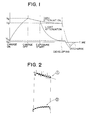
- Fig. 1 which schematically illustrates the state of voltages on the surface of the photosensitive material in electrophotographic processing
- the ordinate represents the potential on the surface of the photosensitive material
- the abscissa represents the time in relation to the processing steps.
- the potential on the surface of the photosensitive material reaches a saturation potential Vs and after the charge is turned OFF, the surface potential decreases due to dark attenuation.
- Vs saturation potential
- the surface potential suddenly decreases on a bright portion L depending upon the sensitivity characteristics of the photosensitive material but the surface potential on a dark portion D remains with dark attenuation.
- the steps of developing and cleaning are carried out.
- the surface potential V D on the dark portion at the time of developing has a relation to the image density, and a difference from the developing bias potential gives a predetermined contrast.
- the potential on the surface of the photosensitive material reaches a certain residual potential V R and, then, the aforementioned steps are repeated.
- the saturation potential V S is usually of the order of from 500 to 1000 V and the residual potential V R , on the other hand, is of the order of from 10 to 80 V, though they may vary depending upon the kind of the photosensitive material.
- the residual potential V R can, in principle, be brought to a value close to zero, it has been considered that as the quantity of light for discharging increases too much, troubles arise due to optical wear and generation of light carriers and there is, on the other hand, virtually no problem if the discharging is effected to a degree of the above-mentioned potential difference.
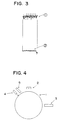
- FIGs. 2 and 3 are graphs illustrating relationships between the potential on the surface of the drum and the surface potential after the discharge by exposure using a positively charged-type organic photosensitive drum having a diameter of 30 mm (for details, refer to Comparative Exampie 1 and Example 1 appearing later) as measured by using a measuring device shown in Fig. 4, and wherein the ordinate represents the potential and the abscissa represents the time.
- curve (1) represents the potential on the surface of the drum
- curve (2) represents the residual potential after the discharge.
- the peaks of the curve (1) correspond to the revolutions of the drum 1.
- Fig. 2 illustrates an example according to the prior art wherein the potential on the surface of the drum is stepwisely decreasing depending upon the number of revolutions of the drum
- Fig. 3 illustrates an example of the present invention wherein the potential on the surface of the drum is prevented from stepwisely decreasing but stably remains stable at a given value irrespective of the number of revolutions.
- the measurement was taken by repeating the charge and discharge by exposure by rotating the positively charged-type organic photosensitive drum 1 which is surrounded as shown in Fig. 4 by a positive corona-charging mechanism, a probe 3 for detecting the surface potential, an exposure/discharge mechanism 4, and a probe 5 for detecting the residual potential after the discharge.
- the amount of discharge is so set that, in forming a copy image, the residual potential is 10% or less of the charged surface potential after the discharge of the first revolution, and an increase in the residual potential is not more than 30% after the discharge of the last revolution. Therefore, the surface potential is prevented from being stepwisely decreased by the number of revolutions, the density of a piece of image is prevented from stepwisely decreasing and, thus, the invention has succeeded in forming an image having uniform density and quality.
- the photosensitive drum has a small diameter with a circumferential length shorter than 1/2 of the image size in the rotating direction of the drum (for example, when a paper of A4 size is used by conveying it in the lengthwise direction of the paper, with a photosensitive drum having a diameter of 40 mm or less, especially 30 mm or less), and a copy image is formed by revolving the drum many times. Therefore, the apparatus, as a whole, can be markedly decreased in size, enabling the personal copying machine to be installed on a compact area or to be realized in a compact volume, lending itself well for being incorporated in a facsimile, a laser printer or a like apparatus.
- a corona charger 9 made up of a tungsten wire 7 and a shielding case 8 is disposed around a drum 6 made of an aluminum blank tube, a high-voltage generating device (HV) 10 is connected to the tungsten wire 7 via an ammeter A1, and the shielding case 8 is grounded via an ammeter A2.
- HV high-voltage generating device
- the drum 6 is connected to the positive side of a bias power source 11 and its negative side is grounded via an ammeter A3.
- a current Icc fed to the wire 7, a current Isc fed to the shielding case 8 and a current Ipc fed to the blank tube 6 were measured while changing the bias voltage.
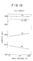
- Figs. 6 to 10 show results when Icc is changed.
- the residual potential, after the discharge is lowered to satisfy the above requirement by increasing the quantity of exposure at the time of discharge by exposure, which is the simplest method. It is, however, also possible to decrease the residual potential after the discharge in a contact manner by applying a bias voltage of a polarity opposite to that of the charged potential.
- an increase in dark attenuation by exposure discharge can be effectively prevented by using a source of monochromatic light of a spectral wavelength exhibited by the photosensitive material and by also effecting the discharge by exposure that the absorption of the light rays takes place on the surface of the photosensitive material.
- the potential on the surface of the drum is furthermore prevented from being stepwisely decreased irrespective of the number of revolutions of the drum, an increase in the dark attenuation is suppressed when the image-forming cycle is repeated many times, the potential of the electrostatic image used for the developing is maintained high, the image of a high density is formed, and abrasion resistance of the photosensitive material is strikingly increased.
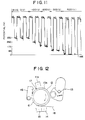
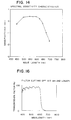
- FIG. 11 shows the measured results of the charged potential (upper side) and the residual potential (lower side) after the discharge using the positively charged-type organic single-layer photosensitive material while changing the applied bias voltage at the time of discharging using a brush, from which it will be understood that the residual potential is adjusted to a predetermined level by setting the bias potential.
- a corona charger 11a for main charging around the drum 6 equipped with a photosensitive layer 10a are arranged a corona charger 11a for main charging, an optical system 12 for exposing to image, a developer 13 using a one-component type developing agent or a two-component type developing agent, a charger 14 for transferring toner, a charger 15 for separating a copy paper sheet, a mechanism 16 for cleaning residual toner, and a source of light 17 for discharging.
- the image is formed according to a process shown in Fig. 1.
- a latent image of surface potential VD of the dark portion is developed with the toner which is charged into an opposite polarity, the toner image is transferred onto a copy paper sheet 18 in an electric field applied by the toner-transferring charger 14, and the copy paper sheet onto which the toner image is transferred is separated by the action of the charger 15 for separation and is sent to the subsequent processing zone such as of a thermally fixing roller (not shown).
- the toner remaining on the photosensitive layer 10 is removed by the cleaning mechanism 16 and is discharged by being exposed to light from the source of light 17.
- a positive image can be formed by effecting the reversal developing using the toner that is charged into the same polarity as the latent image.
- the photosensitive drum used in this invention is a small-diameter drum having a shorter circumferential length than 1/2 of the image size in the rotating direction of the drum (for example, an outer diameter of 40 mm or less, especially as short as 20 to 30 mm).
- the photosensitive drum and the image forming cycle are related to each other so that one image may be formed by many circumferential revolutions of the drum. Furthermore, the photosensitive drum and the image-forming cycle are so related to each other that a copy image is formed after the drum is revolved many times. For example, when the photosensitive drum has a diameter of 30 mm and an image of a size B4 is to be formed, a copy image is formed through four revolutions. When the size is A4R, a copy image is formed through six revolutions. That is, the effect of the present invention is distinctively exhibited when a copy image is to be formed through three or more revolutions.
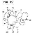
- Fig. 13 illustrates an electrophotographic apparatus according to another embodiment of the present invention.
- This apparatus is the same as the apparatus of Fig. 12 except for the provision of a contact-type discharging mechanism 20 instead of the source of light for discharging and a bias power source 19 for applying a bias voltage of a polarity opposite to that of the charged potential of the photosensitive material.
- An AC discharging may be employed as a discharging mechanism in addition to the above-mentioned discharging by exposure and the contact-type discharging using a brush or a roller.
- the photosensitive material any known photosensitive material can be used such as selenium photosensitive materials (amorphous-selenium type, selenium-tellurium alloy type, selenium-arsenic alloy type, etc.), amorphous silicon photosensitive materials and organic photosensitive materials.
- the organic photosensitive material there can be exemplified an organic laminated-type photosensitive material obtained by laminating a charge generating layer containing a charge generating substance and a charge transporting layer containing a charge transporting substance, and an organic single-layer type photosensitive material obtained by dispersing a charge generating substance in the charge transporting medium.
- the charge generating substance any organic photoconducting pigment that has been widely known can be used.
- the pigments it is desired to use a phthalocyanine type pigment, a perylene type pigment, a quinacridone type pigment, a pyranthrone type pigment, a dis-azo type pigment, a tris-azo type pigment and the like.
- the charge transporting medium the one obtained by dispersing a charge transporting substance in a resin medium is used.
- the charge transporting substance there can be used any widely known positive hole transporting substance or an electron transporting substance to meet the object of the present invention.
- Preferred examples of the positive hole transporting substance include a poly-N-vinyicarbazole, a phenanthrene, an N-ethylcarbazole, a 2,5-diphenyl-1,3,4-oxadiazole, a 2,5-bis(4-diethylaminophenyl)-1,3,4-oxadiazole, a bis-diethylaminophenyl-1,3,6-oxadiazole, a 4,4'-bis(diethylamino)-2,2'-dimethyltriphenylmethane, a 2,4,5-triaminophenylimidazole, a 2,5-bis(4-diethylaminophenyl)-1,3,4-triazo
- Preferred examples of the electron transporting substance include a 2-nitro-9-fluorenone, a 2,7-dinitro-9-fluorenone, a 2,4,7-trinitro-9-fluorenone, a 2,4,5,7-tetranitro-9-fluorenone, a 2-nitrobenzothiophene, a 2,4,8-trinitrothioxanthone, a dinitroanthracene, a dinitroacridine, and a dinitroanthraquinone.
- binder resins there can be exemplified a variety of polymers such as a styrene type polymer, a styrene-butadiene copolymer, a styrene-acrylonitrile copolymer, a styrene-maleic acid copolymer, an acrylic type polymer, a styrene-acrylic type copolymer, a styrene-vinyl acetate copolymer, a polyvinyl chloride, a polyvinyl chloride-vinyl acetate copolymer, a polyester, an alkyd resin, a polyamide, a polyurethane, an epoxy resin, a polycarbonate, a polyarylate, a polysulfone, a diallyl phthalate resin, a silicone resin, a ketone resin, a polyvinyl butyral resin, a polyether resin, a phenol resin, and photo-curing
- the charge generating substance should be contained in the photosensitive layer in an amount of from 0.1 to 50 parts by weight, and particularly from 0.5 to 30 parts by weight per 100 parts by weight of the binder resin.
- the charge transporting substance should be contained in an amount of from 20 to 500 parts by weight, and particularly from 30 to 200 parts by weight, per 100 parts by weight of the binder resin.
- the photosensitive layer should have a thickness of 10 to 40 ⁇ m, and particularly from 22 to 32 ⁇ m, from the standpoint of obtaining a high surface potential and good abrasion resistance and sensitivity.
- the organic photosensitive layer is formed by dissolving the above-mentioned resin in a solvent such as an amide-type solvent, e.g., an N,N-dimethylformamide or an N,N-dimethylacetamide; a cyclic ether such as a tetrahydrofurane or a dioxane; a dimethyl sulfoxide; an aromatic solvent such as a benzene, a toluene or a xylene; ketones such as a methyl ethyl ketone and the like; an N-methyl-2-pyrrolidone; or phenols such as a phenol, a cresol and the like, followed by dispersing a charge generating substance therein to obtain a coating composition.
- This composition is then applied onto the electrically conducting substrate to form the organic photosensitive layer.
- the present invention exhibits distinct advantages when use is made of a positively charged-type organic single-layer photosensitive material.
- the charge generating substance should be a perylene type pigment, an azo type pigment or a combination thereof
- the charge transporting substance should be a diphenoquinone derivative such as a 2,6-dimethyl-2',6'-di-tert-dibutyldiphenoquinone or the like, a diamine type compound such as a 3,3'-dimethyl-N,N,N',N'-tetrakis-4-methylphenyl(1,1'-biphenyl)-4,4'-diamine or the like, a fluorene type compound, or a hydrazone type compound.
- the main charging may be carried out relying upon the corona charging using a corotron or a scorotron, or by using the widely known contact-type charging apparatus with a charging brush, a charging roll or a charging blade.
- the main charging should be so effected that the saturation charged potential (Vs) is from 500 to 1000 V, and particularly from 700 to 850 V.
- the corona charger should apply a voltage of as high as from 4 to 7 KV.
- the charging device In the contact-type charging, on the other hand, the charging device should be impressed with a voltage which is about 1.5 to about 3 times as great as the charge start voltage of the photosensitive material.
- the exposure to image, developing, transfer, separation of copy paper, and cleaning are carried out by widely known means using widely known mechanisms.
- the quantity of light for discharging is 10 times or more, and particularly 20 times or more, as great as the half exposure quantity on the surface of the photosensitive material.
- the discharging lamp there can be used a source of visible light such as a halogen lamp, a fluorescent lamp, a cold cathode tube, a red or a green neon lamp, as well as a source of monochromatic light such as LED of red, yellow or green color.
- the intensity of illumination should be 20 lux ⁇ sec or higher, and preferably 40 lux ⁇ sec or higher, and more preferably from 100 to 300 lux ⁇ sec.
- the intensity of illumination exceeds 500 lux ⁇ sec, on the other hand, adverse effects result such as optical wear and the like.
- the optical wear such as an increase in the dark attenuation can be prevented even when the quantity of light for discharging is great.
- the contact-type discharging uses an electrically conducting brush, roll or blade, and the discharging is effected by bringing it in contact with the photosensitive material.
- the electrically conducting member should, generally, have a resistivity of from 10 1 to 10 8 ⁇ cm and will be made of a variety of resins or rubbers blended with carbon black, metal powder or electrically conducting particles such as Indium-Tin-Oxide or the like.
- the bias voltage applied to the electrically conducting contact member has a polarity opposite to that of the charged potential of the photosensitive material, and has a value of, generally, 50 to 125%, and particularly 60 to 90%, of an absolute value of the charged potential of the photosensitive material.
- the photosensitive material for use in the following Examples was prepared as described below.
- the following composition for a photosensitive layer was dispersed in a paint shaker for 2 hours to prepare a coating solution for forming a single-layer type photosensitive layer.
- the obtained coating solution was dip-applied onto the surface of an aluminum cylinder having an outer diameter of 30 mm, and was dried at 110°C for 30 minutes to form a 30 ⁇ m-thick single-layer type photosensitive layer thereby to obtain a positively charged-type single-layer electrophotosensitive material.
- Bis-azo pigment (following formula (I)) 10 parts by weight 3,3'-Dimethyl-N,N,N',N'-tetrakis-4-methylphenyl(1,1'-biphenyl)-4,4'-diamine 100 parts by weight 3,3'-Dimethyl-5,5'-di-tert-butyl-4,4'-diphenoquinone 50 parts by weight
- Polycarbonate resin 150 parts by weight Dicyclomethane 800 parts by weight
- the single-layer type electrophotosensitive material prepared above was mounted on the apparatus shown in Fig. 4 which is surrounded by a positive corona-charging mechanism 2, a probe 3 for detecting the surface potential, an exposure/discharge mechanism 4, and a probe 5 for detecting the residual potential after the discharge.
- the single-layer type electrophotosensitive material was revolved four times under the following conditions to repeat the discharging by exposure, to measure the surface potential Vsp (V) using the probe 3 for detecting the surface potential, and to measure the residual potential Vrp (V) using the probe 5 for detecting the residual potential after the discharge.
- the results after each revolution were as shown in Table 1.
- Example 3 a light-emitting diode (monochromatic) was used as a discharging light source in conducting the same experiment. The results are shown in Table 3. The half exposure quantity of the photosensitive material when this light source was used was 1.6 Lux ⁇ sec.
- the amount of discharge is so set that the residual potential after the discharge is smaller than a predetermined value, whereby the image density is suppressed from being stepwisely decreased depending upon the number of revolutions of the drum, and the copy image exhibits improved uniformity in the density and improved image quality.
- the surface potential is markedly suppressed from being decreased by the dark attenuation, and the abrasion resistance is greatly improved.
Landscapes
- Physics & Mathematics (AREA)
- General Physics & Mathematics (AREA)
- Health & Medical Sciences (AREA)
- Toxicology (AREA)
- Spectroscopy & Molecular Physics (AREA)
- Photoreceptors In Electrophotography (AREA)
- Control Or Security For Electrophotography (AREA)
- Electrostatic Charge, Transfer And Separation In Electrography (AREA)
- Discharging, Photosensitive Material Shape In Electrophotography (AREA)
Claims (9)
- Appareil électrophotographique pour former une copie d'image sur une feuille (18), comprenant un tambour photosensible (6), un chargeur électrique principal (11a) pour produire un potentiel surfacique chargé sur ledit tambour, un mécanisme d'exposition optique d'image (12) pour former une image latente sur ledit tambour, un mécanisme de développement (13) pour développer ladite image latente et former une image de toner, un mécanisme de transfert (14) pour transférer ladite image de toner sur la feuille, un membre de nettoyage de toner (16) et un moyen de décharge (17) pour décharger ledit tambour ;
dans lequel le tambour photosensible a une longueur circonférentielle extérieure inférieure à la moitié de la dimension de la feuille dans la direction de rotation du tambour, moyennant quoi une copie d'image est formée sur ladite feuille (18) après que ledit tambour a subi plusieurs révolutions, caractérisé en ce que l'ampleur de la décharge effectuée par le moyen de décharge (17) pour former ladite copie d'image est telle qu'après la décharge de la première révolution, le potentiel résiduel vaut 10 % ou moins dudit potentiel surfacique chargé, et qu'après la décharge de la dernière révolution, le potentiel résiduel augmente de pas plus de 30 %. - Appareil électrophotographique selon la revendication 1, dans lequel le matériau photosensible du tambour (6) est un matériau photosensible organique monocouche chargé positivement.
- Appareil électrophotographique selon la revendication 1 ou 2, dans lequel on obtient le matériau photosensible en dispersant une substance générant une charge dans un milieu transportant une charge.
- Appareil électrophotographique selon la revendication 1, 2 ou 3, dans lequel on forme une copie d'image en faisant tourner trois fois ou plus le tambour photosensible (6).
- Appareil électrophotographique selon l'une quelconque des revendications 1 à 4, dans lequel le matériau photosensible est chargé de telle façon que le potentiel chargé de saturation (VS) est compris dans une plage de 500 à 1 000 V.
- Appareil électrophotographique selon l'une quelconque des revendications 1 à 5, dans lequel la décharge est effectuée par exposition à une quantité de lumière qui vaut au moins 10 fois la moitié de la quantité d'exposition du matériau photosensible.
- Appareil électrophotographique selon l'une quelconque des revendications 1 à 6, dans lequel la décharge est effectuée par exposition à une quantité de lumière de 20 lux.s ou plus en utilisant une lampe au tungstène.
- Appareil électrophotographique selon l'une quelconque des revendications 1 à 6, dans lequel la décharge est effectuée par exposition à une lumière en utilisant une source de lumière monochromatique d'une longueur d'onde spectrale à laquelle le matériau photosensible est sensible.
- Appareil électrophotographique selon l'une quelconque des revendications 1 à 5, dans lequel la décharge est effectuée d'une manière par contact en appliquant une tension de polarisation d'une polarité opposée à celle du potentiel chargé.
Applications Claiming Priority (2)
| Application Number | Priority Date | Filing Date | Title |
|---|---|---|---|
| JP4808993 | 1993-03-09 | ||
| JP48089/93 | 1993-03-09 |
Publications (3)
| Publication Number | Publication Date |
|---|---|
| EP0615172A2 EP0615172A2 (fr) | 1994-09-14 |
| EP0615172A3 EP0615172A3 (fr) | 1995-02-15 |
| EP0615172B1 true EP0615172B1 (fr) | 1998-06-17 |
Family
ID=12793600
Family Applications (1)
| Application Number | Title | Priority Date | Filing Date |
|---|---|---|---|
| EP94301656A Expired - Lifetime EP0615172B1 (fr) | 1993-03-09 | 1994-03-09 | Appareil électrophotographique |
Country Status (6)
| Country | Link |
|---|---|
| US (1) | US5530524A (fr) |
| EP (1) | EP0615172B1 (fr) |
| KR (1) | KR940022199A (fr) |
| CN (1) | CN1100531A (fr) |
| CA (1) | CA2118648A1 (fr) |
| DE (1) | DE69411051T2 (fr) |
Families Citing this family (4)
| Publication number | Priority date | Publication date | Assignee | Title |
|---|---|---|---|---|
| US5832342A (en) * | 1996-07-25 | 1998-11-03 | Mita Industrial Co., Ltd. | Image forming machine with a contact type developing device |
| JP6402989B2 (ja) * | 2014-07-25 | 2018-10-10 | 株式会社リコー | 画像形成装置 |
| CN114556231B (zh) * | 2019-10-18 | 2023-06-27 | 佳能株式会社 | 导电性构件、其制造方法、处理盒以及电子照相图像形成设备 |
| JP7661035B2 (ja) | 2020-12-17 | 2025-04-14 | キヤノン株式会社 | 画像形成装置 |
Family Cites Families (7)
| Publication number | Priority date | Publication date | Assignee | Title |
|---|---|---|---|---|
| US4821068A (en) * | 1983-05-10 | 1989-04-11 | Canon Kabushiki Kaisha | Image forming apparatus |
| US4870460A (en) * | 1986-12-05 | 1989-09-26 | Ricoh Company, Ltd. | Method of controlling surface potential of photoconductive element |
| CA1327830C (fr) * | 1988-08-29 | 1994-03-15 | Hiroki Ohba | Methode de deselectrification pour appareil electrophotographique |
| JP2918045B2 (ja) * | 1988-10-28 | 1999-07-12 | 株式会社リコー | 画像濃度制御装置 |
| JPH04174465A (ja) * | 1990-07-25 | 1992-06-22 | Hitachi Ltd | カラー画像電子写真装置 |
| JPH04177376A (ja) * | 1990-11-13 | 1992-06-24 | Minolta Camera Co Ltd | 画像形成装置 |
| EP0613067B1 (fr) * | 1993-02-26 | 1998-08-26 | Mita Industrial Co. Ltd. | Dispositif de transfert dans un appareil de formation d'image |
-
1994
- 1994-03-08 US US08/207,166 patent/US5530524A/en not_active Expired - Lifetime
- 1994-03-09 KR KR1019940004510A patent/KR940022199A/ko not_active Withdrawn
- 1994-03-09 EP EP94301656A patent/EP0615172B1/fr not_active Expired - Lifetime
- 1994-03-09 DE DE69411051T patent/DE69411051T2/de not_active Expired - Fee Related
- 1994-03-09 CA CA002118648A patent/CA2118648A1/fr not_active Abandoned
- 1994-03-09 CN CN94102470A patent/CN1100531A/zh active Pending
Also Published As
| Publication number | Publication date |
|---|---|
| CN1100531A (zh) | 1995-03-22 |
| US5530524A (en) | 1996-06-25 |
| CA2118648A1 (fr) | 1994-09-10 |
| DE69411051D1 (de) | 1998-07-23 |
| EP0615172A3 (fr) | 1995-02-15 |
| KR940022199A (ko) | 1994-10-20 |
| EP0615172A2 (fr) | 1994-09-14 |
| DE69411051T2 (de) | 1999-02-18 |
Similar Documents
| Publication | Publication Date | Title |
|---|---|---|
| JP2010127963A (ja) | 有機感光体、画像形成方法、画像形成装置及びプロセスカートリッジ | |
| JP2009251365A (ja) | 電子写真感光体およびそれを備えた画像形成装置 | |
| JPH07325440A (ja) | 画像形成装置 | |
| JP3257910B2 (ja) | 電子写真法 | |
| EP0615172B1 (fr) | Appareil électrophotographique | |
| JP2008233745A (ja) | 画像形成装置及び画像形成方法 | |
| CN102269955A (zh) | 图像形成装置 | |
| JP2001066800A (ja) | 電子写真感光体、電子写真プロセスカートリッジ、及び電子写真装置 | |
| JP2003107759A (ja) | 画像形成装置 | |
| JPH06318023A (ja) | 電子写真装置 | |
| JP3460285B2 (ja) | 画像形成装置 | |
| US20040185357A1 (en) | Electrophotographic photoreceptor and image forming device | |
| JPH07234618A (ja) | 画像形成装置 | |
| JP3682848B2 (ja) | 電子写真用感光体およびそれを用いる画像形成装置 | |
| JP2003228183A (ja) | 電子写真感光体および画像形成装置 | |
| JP5375304B2 (ja) | 画像形成方法及び画像形成装置 | |
| JPH0743986A (ja) | 画像形成装置 | |
| JP3367318B2 (ja) | 電子写真感光体およびそれを用いた画像形成装置 | |
| JPH08254930A (ja) | 画像形成装置 | |
| JPH0743987A (ja) | 画像形成装置 | |
| JP2001265025A (ja) | 電子写真感光体、及びそれを用いた画像形成方法並びに装置 | |
| JPH07152295A (ja) | 画像形成装置 | |
| JP3227230B2 (ja) | 電子写真装置 | |
| JP3432093B2 (ja) | 画像形成装置 | |
| JP2003066640A (ja) | 感光体および画像形成装置 |
Legal Events
| Date | Code | Title | Description |
|---|---|---|---|
| PUAI | Public reference made under article 153(3) epc to a published international application that has entered the european phase |
Free format text: ORIGINAL CODE: 0009012 |
|
| AK | Designated contracting states |
Kind code of ref document: A2 Designated state(s): DE FR GB IT NL |
|
| PUAL | Search report despatched |
Free format text: ORIGINAL CODE: 0009013 |
|
| AK | Designated contracting states |
Kind code of ref document: A3 Designated state(s): DE FR GB IT NL |
|
| 17P | Request for examination filed |
Effective date: 19950228 |
|
| 17Q | First examination report despatched |
Effective date: 19960904 |
|
| GRAG | Despatch of communication of intention to grant |
Free format text: ORIGINAL CODE: EPIDOS AGRA |
|
| GRAG | Despatch of communication of intention to grant |
Free format text: ORIGINAL CODE: EPIDOS AGRA |
|
| GRAG | Despatch of communication of intention to grant |
Free format text: ORIGINAL CODE: EPIDOS AGRA |
|
| GRAH | Despatch of communication of intention to grant a patent |
Free format text: ORIGINAL CODE: EPIDOS IGRA |
|
| GRAH | Despatch of communication of intention to grant a patent |
Free format text: ORIGINAL CODE: EPIDOS IGRA |
|
| GRAA | (expected) grant |
Free format text: ORIGINAL CODE: 0009210 |
|
| AK | Designated contracting states |
Kind code of ref document: B1 Designated state(s): DE FR GB IT NL |
|
| REF | Corresponds to: |
Ref document number: 69411051 Country of ref document: DE Date of ref document: 19980723 |
|
| ITF | It: translation for a ep patent filed | ||
| ET | Fr: translation filed | ||
| PLBE | No opposition filed within time limit |
Free format text: ORIGINAL CODE: 0009261 |
|
| STAA | Information on the status of an ep patent application or granted ep patent |
Free format text: STATUS: NO OPPOSITION FILED WITHIN TIME LIMIT |
|
| 26N | No opposition filed | ||
| PG25 | Lapsed in a contracting state [announced via postgrant information from national office to epo] |
Ref country code: NL Free format text: LAPSE BECAUSE OF NON-PAYMENT OF DUE FEES Effective date: 19991001 |
|
| PG25 | Lapsed in a contracting state [announced via postgrant information from national office to epo] |
Ref country code: FR Free format text: LAPSE BECAUSE OF NON-PAYMENT OF DUE FEES Effective date: 19991130 |
|
| NLV4 | Nl: lapsed or anulled due to non-payment of the annual fee |
Effective date: 19991001 |
|
| REG | Reference to a national code |
Ref country code: FR Ref legal event code: ST |
|
| REG | Reference to a national code |
Ref country code: GB Ref legal event code: IF02 |
|
| PG25 | Lapsed in a contracting state [announced via postgrant information from national office to epo] |
Ref country code: IT Free format text: LAPSE BECAUSE OF NON-PAYMENT OF DUE FEES Effective date: 20050309 |
|
| PGFP | Annual fee paid to national office [announced via postgrant information from national office to epo] |
Ref country code: DE Payment date: 20090306 Year of fee payment: 16 |
|
| PG25 | Lapsed in a contracting state [announced via postgrant information from national office to epo] |
Ref country code: DE Free format text: LAPSE BECAUSE OF NON-PAYMENT OF DUE FEES Effective date: 20101001 |
|
| PGFP | Annual fee paid to national office [announced via postgrant information from national office to epo] |
Ref country code: GB Payment date: 20120307 Year of fee payment: 19 |
|
| GBPC | Gb: european patent ceased through non-payment of renewal fee |
Effective date: 20130309 |
|
| PG25 | Lapsed in a contracting state [announced via postgrant information from national office to epo] |
Ref country code: GB Free format text: LAPSE BECAUSE OF NON-PAYMENT OF DUE FEES Effective date: 20130309 |