EP0615280A1 - Elektrostatische Halteplatte - Google Patents
Elektrostatische Halteplatte Download PDFInfo
- Publication number
- EP0615280A1 EP0615280A1 EP93301764A EP93301764A EP0615280A1 EP 0615280 A1 EP0615280 A1 EP 0615280A1 EP 93301764 A EP93301764 A EP 93301764A EP 93301764 A EP93301764 A EP 93301764A EP 0615280 A1 EP0615280 A1 EP 0615280A1
- Authority
- EP
- European Patent Office
- Prior art keywords
- insulating layer
- electrostatic chuck
- metal oxide
- transition metal
- alumina
- Prior art date
- Legal status (The legal status is an assumption and is not a legal conclusion. Google has not performed a legal analysis and makes no representation as to the accuracy of the status listed.)
- Granted
Links
Images



Classifications
-
- H—ELECTRICITY
- H02—GENERATION; CONVERSION OR DISTRIBUTION OF ELECTRIC POWER
- H02N—ELECTRIC MACHINES NOT OTHERWISE PROVIDED FOR
- H02N13/00—Clutches or holding devices using electrostatic attraction, e.g. using Johnson-Rahbek effect
-
- B—PERFORMING OPERATIONS; TRANSPORTING
- B32—LAYERED PRODUCTS
- B32B—LAYERED PRODUCTS, i.e. PRODUCTS BUILT-UP OF STRATA OF FLAT OR NON-FLAT, e.g. CELLULAR OR HONEYCOMB, FORM
- B32B18/00—Layered products essentially comprising ceramics, e.g. refractory products
-
- C—CHEMISTRY; METALLURGY
- C04—CEMENTS; CONCRETE; ARTIFICIAL STONE; CERAMICS; REFRACTORIES
- C04B—LIME, MAGNESIA; SLAG; CEMENTS; COMPOSITIONS THEREOF, e.g. MORTARS, CONCRETE OR LIKE BUILDING MATERIALS; ARTIFICIAL STONE; CERAMICS; REFRACTORIES; TREATMENT OF NATURAL STONE
- C04B35/00—Shaped ceramic products characterised by their composition; Ceramics compositions; Processing powders of inorganic compounds preparatory to the manufacturing of ceramic products
- C04B35/622—Forming processes; Processing powders of inorganic compounds preparatory to the manufacturing of ceramic products
- C04B35/626—Preparing or treating the powders individually or as batches ; preparing or treating macroscopic reinforcing agents for ceramic products, e.g. fibres; mechanical aspects section B
- C04B35/63—Preparing or treating the powders individually or as batches ; preparing or treating macroscopic reinforcing agents for ceramic products, e.g. fibres; mechanical aspects section B using additives specially adapted for forming the products, e.g.. binder binders
-
- C—CHEMISTRY; METALLURGY
- C04—CEMENTS; CONCRETE; ARTIFICIAL STONE; CERAMICS; REFRACTORIES
- C04B—LIME, MAGNESIA; SLAG; CEMENTS; COMPOSITIONS THEREOF, e.g. MORTARS, CONCRETE OR LIKE BUILDING MATERIALS; ARTIFICIAL STONE; CERAMICS; REFRACTORIES; TREATMENT OF NATURAL STONE
- C04B35/00—Shaped ceramic products characterised by their composition; Ceramics compositions; Processing powders of inorganic compounds preparatory to the manufacturing of ceramic products
- C04B35/622—Forming processes; Processing powders of inorganic compounds preparatory to the manufacturing of ceramic products
- C04B35/626—Preparing or treating the powders individually or as batches ; preparing or treating macroscopic reinforcing agents for ceramic products, e.g. fibres; mechanical aspects section B
- C04B35/63—Preparing or treating the powders individually or as batches ; preparing or treating macroscopic reinforcing agents for ceramic products, e.g. fibres; mechanical aspects section B using additives specially adapted for forming the products, e.g.. binder binders
- C04B35/632—Organic additives
- C04B35/634—Polymers
- C04B35/63404—Polymers obtained by reactions only involving carbon-to-carbon unsaturated bonds
- C04B35/6342—Polyvinylacetals, e.g. polyvinylbutyral [PVB]
-
- H—ELECTRICITY
- H10—SEMICONDUCTOR DEVICES; ELECTRIC SOLID-STATE DEVICES NOT OTHERWISE PROVIDED FOR
- H10P—GENERIC PROCESSES OR APPARATUS FOR THE MANUFACTURE OR TREATMENT OF DEVICES COVERED BY CLASS H10
- H10P72/00—Handling or holding of wafers, substrates or devices during manufacture or treatment thereof
- H10P72/70—Handling or holding of wafers, substrates or devices during manufacture or treatment thereof for supporting or gripping
- H10P72/72—Handling or holding of wafers, substrates or devices during manufacture or treatment thereof for supporting or gripping using electrostatic chucks
- H10P72/722—Details of electrostatic chucks
-
- C—CHEMISTRY; METALLURGY
- C04—CEMENTS; CONCRETE; ARTIFICIAL STONE; CERAMICS; REFRACTORIES
- C04B—LIME, MAGNESIA; SLAG; CEMENTS; COMPOSITIONS THEREOF, e.g. MORTARS, CONCRETE OR LIKE BUILDING MATERIALS; ARTIFICIAL STONE; CERAMICS; REFRACTORIES; TREATMENT OF NATURAL STONE
- C04B2235/00—Aspects relating to ceramic starting mixtures or sintered ceramic products
- C04B2235/65—Aspects relating to heat treatments of ceramic bodies such as green ceramics or pre-sintered ceramics, e.g. burning, sintering or melting processes
- C04B2235/656—Aspects relating to heat treatments of ceramic bodies such as green ceramics or pre-sintered ceramics, e.g. burning, sintering or melting processes characterised by specific heating conditions during heat treatment
-
- C—CHEMISTRY; METALLURGY
- C04—CEMENTS; CONCRETE; ARTIFICIAL STONE; CERAMICS; REFRACTORIES
- C04B—LIME, MAGNESIA; SLAG; CEMENTS; COMPOSITIONS THEREOF, e.g. MORTARS, CONCRETE OR LIKE BUILDING MATERIALS; ARTIFICIAL STONE; CERAMICS; REFRACTORIES; TREATMENT OF NATURAL STONE
- C04B2235/00—Aspects relating to ceramic starting mixtures or sintered ceramic products
- C04B2235/65—Aspects relating to heat treatments of ceramic bodies such as green ceramics or pre-sintered ceramics, e.g. burning, sintering or melting processes
- C04B2235/656—Aspects relating to heat treatments of ceramic bodies such as green ceramics or pre-sintered ceramics, e.g. burning, sintering or melting processes characterised by specific heating conditions during heat treatment
- C04B2235/6567—Treatment time
-
- C—CHEMISTRY; METALLURGY
- C04—CEMENTS; CONCRETE; ARTIFICIAL STONE; CERAMICS; REFRACTORIES
- C04B—LIME, MAGNESIA; SLAG; CEMENTS; COMPOSITIONS THEREOF, e.g. MORTARS, CONCRETE OR LIKE BUILDING MATERIALS; ARTIFICIAL STONE; CERAMICS; REFRACTORIES; TREATMENT OF NATURAL STONE
- C04B2237/00—Aspects relating to ceramic laminates or to joining of ceramic articles with other articles by heating
- C04B2237/30—Composition of layers of ceramic laminates or of ceramic or metallic articles to be joined by heating, e.g. Si substrates
- C04B2237/32—Ceramic
- C04B2237/34—Oxidic
-
- C—CHEMISTRY; METALLURGY
- C04—CEMENTS; CONCRETE; ARTIFICIAL STONE; CERAMICS; REFRACTORIES
- C04B—LIME, MAGNESIA; SLAG; CEMENTS; COMPOSITIONS THEREOF, e.g. MORTARS, CONCRETE OR LIKE BUILDING MATERIALS; ARTIFICIAL STONE; CERAMICS; REFRACTORIES; TREATMENT OF NATURAL STONE
- C04B2237/00—Aspects relating to ceramic laminates or to joining of ceramic articles with other articles by heating
- C04B2237/30—Composition of layers of ceramic laminates or of ceramic or metallic articles to be joined by heating, e.g. Si substrates
- C04B2237/32—Ceramic
- C04B2237/34—Oxidic
- C04B2237/343—Alumina or aluminates
-
- C—CHEMISTRY; METALLURGY
- C04—CEMENTS; CONCRETE; ARTIFICIAL STONE; CERAMICS; REFRACTORIES
- C04B—LIME, MAGNESIA; SLAG; CEMENTS; COMPOSITIONS THEREOF, e.g. MORTARS, CONCRETE OR LIKE BUILDING MATERIALS; ARTIFICIAL STONE; CERAMICS; REFRACTORIES; TREATMENT OF NATURAL STONE
- C04B2237/00—Aspects relating to ceramic laminates or to joining of ceramic articles with other articles by heating
- C04B2237/30—Composition of layers of ceramic laminates or of ceramic or metallic articles to be joined by heating, e.g. Si substrates
- C04B2237/32—Ceramic
- C04B2237/34—Oxidic
- C04B2237/345—Refractory metal oxides
-
- C—CHEMISTRY; METALLURGY
- C04—CEMENTS; CONCRETE; ARTIFICIAL STONE; CERAMICS; REFRACTORIES
- C04B—LIME, MAGNESIA; SLAG; CEMENTS; COMPOSITIONS THEREOF, e.g. MORTARS, CONCRETE OR LIKE BUILDING MATERIALS; ARTIFICIAL STONE; CERAMICS; REFRACTORIES; TREATMENT OF NATURAL STONE
- C04B2237/00—Aspects relating to ceramic laminates or to joining of ceramic articles with other articles by heating
- C04B2237/30—Composition of layers of ceramic laminates or of ceramic or metallic articles to be joined by heating, e.g. Si substrates
- C04B2237/32—Ceramic
- C04B2237/34—Oxidic
- C04B2237/345—Refractory metal oxides
- C04B2237/346—Titania or titanates
-
- Y—GENERAL TAGGING OF NEW TECHNOLOGICAL DEVELOPMENTS; GENERAL TAGGING OF CROSS-SECTIONAL TECHNOLOGIES SPANNING OVER SEVERAL SECTIONS OF THE IPC; TECHNICAL SUBJECTS COVERED BY FORMER USPC CROSS-REFERENCE ART COLLECTIONS [XRACs] AND DIGESTS
- Y10—TECHNICAL SUBJECTS COVERED BY FORMER USPC
- Y10T—TECHNICAL SUBJECTS COVERED BY FORMER US CLASSIFICATION
- Y10T279/00—Chucks or sockets
- Y10T279/23—Chucks or sockets with magnetic or electrostatic means
Definitions
- the present invention relates to an electrostatic chuck used to attractively fix articles such as semiconductor wafers by electrostatic force.
- Electrostatic chucks provided with an internal electrode between a substrate and an insulating layer (dielectric layer) are used as wafer fixing jigs when semiconductor wafers are treated by plasma etching, CVD, ion plating or the like.
- Such electrostatic chucks are required to perform so that a great electrostatic attractive force is produced during the application of voltage so that the attracted articles are prevented from falling, and that after removing the applied voltage the electrostatic attractive force is immediately decreased so that the attracted articles can be displaced with ease.
- Means for increasing the electrostatic attractive force include, for example, means in which the insulating layer has a large dielectric constant (Japanese Patent Publications No. 60-59104 and No. 62-19060), the thickness of the insulating layer is controlled (Japanese Patent Laid-open Publication No. 57-64950) and the insulating layer has a volume resistivity in a given range (Japanese Patent Publication No. 61-14660 and Japanese Patent Laid-open Publication No. 2-22166).
- Means for making the displacement of attracted articles easy include, for example, means in which helium gas is blown between the chuck surface and an attracted article (Japanese Utility Model Laid-open Publication No. 2-120831) and applying a voltage with a polarity opposite to the voltage applied when the wafers are attracted (Japanese Patent Publication No. 2-63304).
- the means for increasing the electrostatic attractive force rely only on the insulating layer, where the residual attractive force tends to become larger with an increase in electrostatic attractive force. Furthermore, with such means it takes as long as at least 60 seconds before the residual attractive force attenuates and the attracted article can be displaced with ease. This is unsuitable for those instances in which attracted articles should be displaced immediately after treatment. Hence, in such cases there is the disadvantage that other devices or additional operations other than the usual operations have to be used in order to make the displacement of attracted articles easy. In particular, there is a problem when such devices are used in a low temperature environment.
- the materials constituting the insulating layer (dielectric layer) of conventional electrostatic chucks do not allow its volume resistivity to be arbitrarily controllable over a wide range.
- titania to alumina as a transition metal oxide.
- composite oxide grains deposited between alumina grains increase with an increase in the amount of titania added, resulting in a remarkable dependence of electrical conductivity on electric field intensity. ie. the volume resistivity abruptly decreases at a certain electric field intensity that forms a border, making it impossible to maintain given electrostatic performance.
- an object of the present invention is to provide an electrostatic chuck that allows arbitrary control of the volume resistivity of the insulating layer over a wide range during its manufacture and which can hence exhibit a stable electrostatic performance without regard to operating temperatures.
- the present invention provides an electrostatic chuck comprising a substrate and formed thereon an internal electrode and an insulating layer, said insulating layer comprising a solid-solution which comprises alumina and a transition metal oxide having the structure of a corundum.
- the insulating layer preferably also comprises a glass component.
- the insulating layer may comprise grains of the solid solution with the glass component present in the grain boundaries of the solid solution grains.
- the insulating layer preferably comprises not more than 2% by weight of another transition metal oxide, preferably not having a corundum structure. Particularly preferred is titania TiO2. This is particularly preferred in addition to a glass component, in which case the insulating layer may comprise grains of the solid solution, a glass component present in the grain boundaries of the solid solution grains and not more than 2% by weight of a transition metal oxide preferably deposited in the grain boundaries of the solid solution grains.
- the insulating layer preferably has a volume resistivity of not higher than 1011 ⁇ .m.
- the transition metal oxide herein used has the structure of a corundum. Since this corundum structure is similar to the crystal structure of alumina, the transition metal oxide can readily form a solid solution with alumina. Such a transition metal oxide may preferably be one of those capable of forming a solid solution with alumina and preferably may be chromia (Cr2O3), Ga2O3, Fe2O3, V2O3, Rh2O3 or Ti2O3. Chromia (Cr2O3) is particularly preferred.
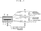
- the electrostatic chuck As shown in Fig. 1, the electrostatic chuck according to the present invention comprises a substrate 1, an insulating layer 2 formed thereon, an internal electrode 3 formed between the substrate 1 and the insulating layer 2.
- the electrode 3 is connected to a DC power source 5 through a lead wire 4 and a semiconductor wafer W is directly connected to ground or electrically connected therewith by a plasma.
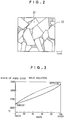
- the insulating layer 2 comprises solid-solution grains 21 comprising alumina and a transition metal oxide, and glass 22 present in grain boundaries of the solid-solution grains.
- the transition metal oxide may preferably include those capable of forming a solid solution with alumina, specifically including chromia, Ga2O3, Fe2O3, V2O3, Rh2O3 and Ti2O3. Chromia (Cr2O3) is particularly preferred, which well assumes the crystal structure of a corundum, the crystal structure of which is similar to alumina.
- Fig. 3 shows the state of solid solution of alumina (Al2O3) and chromia (Cr2O3). As is seen from Fig. 3, a perfect solid solution is formed.
- the present inventor has devised an equivalent circuit of the electrostatic chuck, and has elucidated from the equivalent circuit the relationship between i) attenuation time t s (the time required for residual electrostatic force to attenuate by 98% with respect to the saturated electrostatic force), ii) volume resistivity ⁇ ( ⁇ .m) of the insulating layer at operating temperatures of the electrostatic chuck, iii) dielectric constant ⁇ r of the insulating layer at operating temperatures of the electrostatic chuck, iv) distance d (m) between the internal electrode and the surface of the insulating layer and (v) gap ⁇ (m) between attracted article and the surface of the
- ⁇ a volume resistivity ( ⁇ .m) of the insulating layer
- ⁇ r a dielectric constant of the insulating layer at operating temperatures of the electrostatic chuck
- d is a distance (m) between the internal electrode and the surface of the insulating layer (i.e. thickness of the insulating layer)
- ⁇ is the gap (m) between an attracted article and the surface of the insulating layer.
- Alumina is presumed to have a volume resistivity of 1012 ⁇ .m or more, and chromia a volume resistivity of 104 ⁇ .m or less. Furthermore, as stated above, alumina and chromia can be formed into a perfect solid solution. Hence, the volume resistivity of the insulating layer 2 can be controlled by changing the proportion of the chromia to be added.
- Fig. 4 is a graph showing the relationship between the proportion of chromia in the solid solution and its volume resistivity. As is seen from the graph, the volume resistivity of the insulating layer 2 can be arbitrarily controlled in a given range.
- the solid-solution grains 21 have a lower resistivity than the grain boundary glass 22, so that electric charges are conducted through the solid-solution grains 21.
- electric currents flow according to Ohm's law even when the electric field intensity increases. Hence, no insulation failure occurs even with an abrupt increase in electric currents, so that an damage of silicon wafers can be prevented.
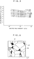
- Fig. 6 is a partial enlarged diagrammatic view of an insulating layer according to another embodiment of the present invention.
- the insulating layer 2 comprises solid-solution grains 21 comprising alumina and chromia (the transition metal oxide having the structure of a corundum), glass 22 present in the grain boundaries of the solid-solution grains, and deposits 23 of titania (TiO2), a transition metal oxide having no corundum structure.
- Fig. 7 is a graph showing the relationship between the concentration of titania (TiO2) and volume resistivity.
- Fig. 8 is a graph showing the relationship between the concentration of titania (TiO2), the volume resistivity of an insulator, and electric field intensity.
- the titania (TiO2), when added is in a concentration of 2% by weight or less, resulting in a great dependence of volume resistivity on electric field intensity to tend to cause insulation failure due to abrupt increase in electric currents.
- the electrostatic chuck according to the present invention can be manufactured in the manner described below.
- alumina powder and the transition metal oxide (chromia, Cr2O3) having the corundum structure, and preferably also titania (TiO2) and a sintering aid that forms the glass component in the final product are made ready for use. These are weighed and then mixed and pulverised using a ball mill.
- a binder such as polyvinyl butyral (PVB) and a solvent such as toluene, isopropyl alcohol or n-butanol are added, followed by deaeration, aging and molding to form a green sheet.
- PVB polyvinyl butyral
- solvent such as toluene, isopropyl alcohol or n-butanol
- the green sheet thus formed is laminated to an unfired substrate made of Al2O3 or the like (the same material as used in the insulating layer) on which an electrode layer comprising tungsten, molybdenum or the like has been printed, followed by firing in a reducing atmosphere at about 1,500°C to about 1,650°C (usually at about 1,600°C) for about 1 hour to about 7 hours (usually about 2 hours).
- a reducing atmosphere at about 1,500°C to about 1,650°C (usually at about 1,600°C) for about 1 hour to about 7 hours (usually about 2 hours).
- the alumina may be added in an amount of from 41 to 91% by weight.
- the transition metal oxide having the corundum structure should conveniently be added in an amount of from 1% by weight to 50% by weight. The reason therefor is that its addition in an amount less than 1% by weight can not be effective and its addition in an amount more than 50% by weight makes it impossible to carry out satisfactory firing.
- As the sintering aid silica sand, clay, glass frit, a carbonate or nitrate of an alkaline earth metal such as MgCO3, CaCO3, SrCO3 or BaCO3 may be used, which should conveniently be added in an amount of from 5% by weight to 12% by weight.
- the electrostatic chucks used in the measurement were prepared by mixing and pulverizing alumina, chromia (Cr2O3) and titania (TiO2) used in the amounts (% by weight) shown in Table 1 and 9% by weight, in terms of oxide, of MgO and CaO as sintering aids in a ball mill, and adding PVB as a binder and toluene and butyl acetate to the resulting powdery mixture, followed by deaeration, aging and molding to form a green sheet.
- alumina chromia
- TiO2 titania
- the green sheet thus formed was laminated to a substrate made of Al2O3, having been similarly formed into a green sheet and on which an electrode layer comprising tungsten had been printed, followed by firing in a reducing atmosphere of a hydrogen-nitrogen mixed gas at 1,600°C for 2 hours.
- the electrostatic chucks according to the present invention have an insulating layer comprising i) solid-solution grains comprising alumina and a transition metal oxide having the structure of a corundum, and preferably a glass component present in grain boundaries of the solid-solution grains, or ii) solid-solution grains comprising alumina and a transition metal oxide having the structure of a corundum, and preferably a glass component present in grain boundaries of the solid-solution grains and not more than 2% by weight of a transition metal oxide deposited in the grain boundaries of the solid-solution grains, it is possible to obtain an electrostatic chuck that allows arbitrary control of the volume resistivity of the insulating layer over a wide range during its manufacture and hence can exhibit a stable electrostatic performance without regard to operating temperatures.
Landscapes
- Chemical & Material Sciences (AREA)
- Engineering & Computer Science (AREA)
- Ceramic Engineering (AREA)
- Manufacturing & Machinery (AREA)
- Inorganic Chemistry (AREA)
- Materials Engineering (AREA)
- Structural Engineering (AREA)
- Organic Chemistry (AREA)
- Chemical Kinetics & Catalysis (AREA)
- Container, Conveyance, Adherence, Positioning, Of Wafer (AREA)
Priority Applications (3)
| Application Number | Priority Date | Filing Date | Title |
|---|---|---|---|
| US08/024,626 US5384681A (en) | 1993-03-01 | 1993-03-01 | Electrostatic chuck |
| EP93301764A EP0615280B1 (de) | 1993-03-01 | 1993-03-09 | Elektrostatische Halteplatte |
| DE1993626535 DE69326535T2 (de) | 1993-03-09 | 1993-03-09 | Elektrostatische Halteplatte |
Applications Claiming Priority (2)
| Application Number | Priority Date | Filing Date | Title |
|---|---|---|---|
| US08/024,626 US5384681A (en) | 1993-03-01 | 1993-03-01 | Electrostatic chuck |
| EP93301764A EP0615280B1 (de) | 1993-03-01 | 1993-03-09 | Elektrostatische Halteplatte |
Publications (2)
| Publication Number | Publication Date |
|---|---|
| EP0615280A1 true EP0615280A1 (de) | 1994-09-14 |
| EP0615280B1 EP0615280B1 (de) | 1999-09-22 |
Family
ID=26134213
Family Applications (1)
| Application Number | Title | Priority Date | Filing Date |
|---|---|---|---|
| EP93301764A Expired - Lifetime EP0615280B1 (de) | 1993-03-01 | 1993-03-09 | Elektrostatische Halteplatte |
Country Status (2)
| Country | Link |
|---|---|
| US (1) | US5384681A (de) |
| EP (1) | EP0615280B1 (de) |
Cited By (5)
| Publication number | Priority date | Publication date | Assignee | Title |
|---|---|---|---|---|
| EP0762491A3 (de) * | 1995-08-31 | 1998-07-29 | Tocalo Co. Ltd. | Elektrostatische Haltevorrichtung und Herstellungsverfahren derselben |
| WO1999029030A1 (en) * | 1997-12-02 | 1999-06-10 | Applied Materials, Inc. | Improved ceramic electrostatic chuck and method of fabricating same |
| EP0806798A3 (de) * | 1996-05-08 | 1999-11-17 | Applied Materials, Inc. | Substratträger mit einer Schicht zur Aufhaltung von Verunreinigungen und Verfahren zu dessen Herstellung |
| WO2001032114A1 (en) * | 1999-11-02 | 2001-05-10 | Wizcare Ltd. | Skin-gripper |
| EP1852907A1 (de) * | 1999-05-25 | 2007-11-07 | Toto Ltd. | Elektrostatisches Futter und Verarbeitungsvorrichtung |
Families Citing this family (11)
| Publication number | Priority date | Publication date | Assignee | Title |
|---|---|---|---|---|
| KR100260587B1 (ko) * | 1993-06-01 | 2000-08-01 | 히가시 데쓰로 | 정전척 및 그의 제조방법 |
| US5535090A (en) * | 1994-03-03 | 1996-07-09 | Sherman; Arthur | Electrostatic chuck |
| US5701228A (en) * | 1995-03-17 | 1997-12-23 | Tokyo Electron Limited | Stage system or device |
| JP3457477B2 (ja) * | 1995-09-06 | 2003-10-20 | 日本碍子株式会社 | 静電チャック |
| US5864459A (en) * | 1996-08-14 | 1999-01-26 | Virginia Tech Intellectual Properties, Inc. | Process for providing a glass dielectric layer on an electrically conductive substrate and electrostatic chucks made by the process |
| WO1998047176A1 (en) * | 1997-04-11 | 1998-10-22 | The Morgan Crucible Company Plc | Composite ceramic dielectrics |
| US5880924A (en) * | 1997-12-01 | 1999-03-09 | Applied Materials, Inc. | Electrostatic chuck capable of rapidly dechucking a substrate |
| US6641939B1 (en) | 1998-07-01 | 2003-11-04 | The Morgan Crucible Company Plc | Transition metal oxide doped alumina and methods of making and using |
| TWI254403B (en) * | 2000-05-19 | 2006-05-01 | Ngk Insulators Ltd | Electrostatic clamper, and electrostatic attracting structures |
| CN105448793A (zh) * | 2014-06-12 | 2016-03-30 | 北京北方微电子基地设备工艺研究中心有限责任公司 | 一种半导体加工设备 |
| JP7241540B2 (ja) * | 2018-12-28 | 2023-03-17 | 東京エレクトロン株式会社 | 測定方法及び測定治具 |
Citations (2)
| Publication number | Priority date | Publication date | Assignee | Title |
|---|---|---|---|---|
| US4735926A (en) * | 1985-03-15 | 1988-04-05 | Ngk Spark Plug Co., Ltd. | Alumina ceramic body |
| EP0339903A1 (de) * | 1988-04-26 | 1989-11-02 | Toto Ltd. | Verfahren zur Herstellung dielektrischer Keramik für elektrostatische Haltevorrichtungen |
Family Cites Families (21)
| Publication number | Priority date | Publication date | Assignee | Title |
|---|---|---|---|---|
| US3875119A (en) * | 1970-12-22 | 1975-04-01 | Hiroshi Aoki | Product and process of producing biaxially oriented insulating film of polyethylene-2,6-naphthalate |
| US4020234A (en) * | 1974-01-02 | 1977-04-26 | International Business Machines Corporation | High-alumina content compositions containing BaO-MgO-SiO2 glass and sintered ceramic articles made therefrom |
| US4040827A (en) * | 1975-10-29 | 1977-08-09 | Xerox Corporation | Development imaging methods |
| US4109377A (en) * | 1976-02-03 | 1978-08-29 | International Business Machines Corporation | Method for preparing a multilayer ceramic |
| US4292261A (en) * | 1976-06-30 | 1981-09-29 | Japan Synthetic Rubber Company Limited | Pressure sensitive conductor and method of manufacturing the same |
| US4384918A (en) * | 1980-09-30 | 1983-05-24 | Fujitsu Limited | Method and apparatus for dry etching and electrostatic chucking device used therein |
| US4361732A (en) * | 1981-02-09 | 1982-11-30 | Northern Telecom Limited | Trunk interface circuit with current compensation |
| GB2106325A (en) * | 1981-09-14 | 1983-04-07 | Philips Electronic Associated | Electrostatic chuck |
| JPS6059104B2 (ja) * | 1982-02-03 | 1985-12-23 | 株式会社東芝 | 静電チヤツク板 |
| JPS5944797A (ja) * | 1982-09-07 | 1984-03-13 | 増田 閃一 | 物体の静電的処理装置 |
| JPS5957446A (ja) * | 1982-09-28 | 1984-04-03 | Kokusai Electric Co Ltd | 静電吸着式基板保持装置 |
| GB2154365A (en) * | 1984-02-10 | 1985-09-04 | Philips Electronic Associated | Loading semiconductor wafers on an electrostatic chuck |
| US4692836A (en) * | 1983-10-31 | 1987-09-08 | Toshiba Kikai Kabushiki Kaisha | Electrostatic chucks |
| JPS60176967A (ja) * | 1984-02-21 | 1985-09-11 | 日本特殊陶業株式会社 | アルミナ磁器組成物 |
| JPS6131636U (ja) * | 1984-07-31 | 1986-02-26 | 株式会社 徳田製作所 | 静電チヤツク |
| FR2568722B1 (fr) * | 1984-08-03 | 1987-10-23 | Thomson Csf | Substrat en ceramique dielectrique et procede d'obtention |
| JPH0697675B2 (ja) * | 1985-10-21 | 1994-11-30 | 東陶機器株式会社 | 静電チャック基盤 |
| US4678683A (en) * | 1985-12-13 | 1987-07-07 | General Electric Company | Process for cofiring structure comprised of ceramic substrate and refractory metal metallization |
| US4769294A (en) * | 1986-11-26 | 1988-09-06 | Ceramics Process Systems Corp. | Alumina materials for low temperature co-sintering with refractory metallization |
| US4724510A (en) * | 1986-12-12 | 1988-02-09 | Tegal Corporation | Electrostatic wafer clamp |
| JP2665242B2 (ja) * | 1988-09-19 | 1997-10-22 | 東陶機器株式会社 | 静電チャック |
-
1993
- 1993-03-01 US US08/024,626 patent/US5384681A/en not_active Expired - Lifetime
- 1993-03-09 EP EP93301764A patent/EP0615280B1/de not_active Expired - Lifetime
Patent Citations (2)
| Publication number | Priority date | Publication date | Assignee | Title |
|---|---|---|---|---|
| US4735926A (en) * | 1985-03-15 | 1988-04-05 | Ngk Spark Plug Co., Ltd. | Alumina ceramic body |
| EP0339903A1 (de) * | 1988-04-26 | 1989-11-02 | Toto Ltd. | Verfahren zur Herstellung dielektrischer Keramik für elektrostatische Haltevorrichtungen |
Non-Patent Citations (1)
| Title |
|---|
| CHEMICAL ABSTRACTS, vol. 117, no. 12, 1992, Columbus, Ohio, US; abstract no. 122716t, T. WATANABE ET AL 'Electrostatic force and absorption current of alumina electrostatic chuck'; & JAPANESE JOURNAL OF APPLIED PHYSICS vol. 31, no. 7, JAPAN pages 2145 - 2150 * |
Cited By (7)
| Publication number | Priority date | Publication date | Assignee | Title |
|---|---|---|---|---|
| EP0762491A3 (de) * | 1995-08-31 | 1998-07-29 | Tocalo Co. Ltd. | Elektrostatische Haltevorrichtung und Herstellungsverfahren derselben |
| KR100268052B1 (ko) * | 1995-08-31 | 2000-10-16 | 나카히라 아키라 | 정전 척부재 및 그 제조방법 |
| EP0806798A3 (de) * | 1996-05-08 | 1999-11-17 | Applied Materials, Inc. | Substratträger mit einer Schicht zur Aufhaltung von Verunreinigungen und Verfahren zu dessen Herstellung |
| WO1999029030A1 (en) * | 1997-12-02 | 1999-06-10 | Applied Materials, Inc. | Improved ceramic electrostatic chuck and method of fabricating same |
| EP1852907A1 (de) * | 1999-05-25 | 2007-11-07 | Toto Ltd. | Elektrostatisches Futter und Verarbeitungsvorrichtung |
| WO2001032114A1 (en) * | 1999-11-02 | 2001-05-10 | Wizcare Ltd. | Skin-gripper |
| WO2001032121A3 (en) * | 1999-11-02 | 2001-11-22 | Wizcare Ltd | Skin-gripper |
Also Published As
| Publication number | Publication date |
|---|---|
| EP0615280B1 (de) | 1999-09-22 |
| US5384681A (en) | 1995-01-24 |
Similar Documents
| Publication | Publication Date | Title |
|---|---|---|
| EP0615280A1 (de) | Elektrostatische Halteplatte | |
| US5384682A (en) | Electrostatic chuck | |
| EP0339903B1 (de) | Verfahren zur Herstellung dielektrischer Keramik für elektrostatische Haltevorrichtungen | |
| EP0415750B1 (de) | Dünnfilmkondensatoren und deren Herstellungsverfahren | |
| US5382469A (en) | Ceramic-titanium nitride electrostatic chuck | |
| Sumita et al. | Degradation of multilayer ceramic capacitors with nickel electrodes | |
| DE69302028T2 (de) | Elektrostatische isolierte Spannvorrichtung und Erregunsgsverfahren | |
| US6641939B1 (en) | Transition metal oxide doped alumina and methods of making and using | |
| WO2011145598A1 (ja) | Esd保護デバイス | |
| KR960035952A (ko) | 스테이지 장치 | |
| JPS6395644A (ja) | 静電チヤツク | |
| EP0412167B1 (de) | Halbleiterkeramikkondensator von dem laminierten typ mit zwischenkornisolation und verfahren zu seiner herstellung | |
| US5091820A (en) | Ceramic piezoelectric element with electrodes formed by reduction | |
| Yoo et al. | Electrical conduction mechanisms of barium-titanate-based thick-film capacitors | |
| EP0256405B1 (de) | Keramische Halbleiterzusammensetzung | |
| EP0429653B1 (de) | Keramischer kondensator eines halbleitertyps mit laminierten und kornisolierten grenzschichten | |
| WO2002093618A3 (en) | Semiconductor structure including low-leakage, high crystalline dielectric | |
| JP2001345161A (ja) | チップ型サージアブソーバおよびその製造方法 | |
| JP3084869B2 (ja) | 静電チャック | |
| EP0506537A1 (de) | Elektrostatische Halteplatte | |
| JPH09293774A (ja) | 静電チャック | |
| JPH05243367A (ja) | 静電チャック | |
| US6444504B1 (en) | Multilayer ZnO polycrystallin diode | |
| US4987515A (en) | Ceramic capacitor with electrodes formed by reduction | |
| KR100279149B1 (ko) | 정전처크 |
Legal Events
| Date | Code | Title | Description |
|---|---|---|---|
| PUAI | Public reference made under article 153(3) epc to a published international application that has entered the european phase |
Free format text: ORIGINAL CODE: 0009012 |
|
| AK | Designated contracting states |
Kind code of ref document: A1 Designated state(s): CH DE FR GB IT LI NL |
|
| 17P | Request for examination filed |
Effective date: 19950206 |
|
| 17Q | First examination report despatched |
Effective date: 19961022 |
|
| GRAG | Despatch of communication of intention to grant |
Free format text: ORIGINAL CODE: EPIDOS AGRA |
|
| GRAG | Despatch of communication of intention to grant |
Free format text: ORIGINAL CODE: EPIDOS AGRA |
|
| GRAG | Despatch of communication of intention to grant |
Free format text: ORIGINAL CODE: EPIDOS AGRA |
|
| GRAH | Despatch of communication of intention to grant a patent |
Free format text: ORIGINAL CODE: EPIDOS IGRA |
|
| GRAH | Despatch of communication of intention to grant a patent |
Free format text: ORIGINAL CODE: EPIDOS IGRA |
|
| GRAA | (expected) grant |
Free format text: ORIGINAL CODE: 0009210 |
|
| AK | Designated contracting states |
Kind code of ref document: B1 Designated state(s): CH DE FR GB IT LI NL |
|
| PG25 | Lapsed in a contracting state [announced via postgrant information from national office to epo] |
Ref country code: LI Free format text: LAPSE BECAUSE OF FAILURE TO SUBMIT A TRANSLATION OF THE DESCRIPTION OR TO PAY THE FEE WITHIN THE PRESCRIBED TIME-LIMIT Effective date: 19990922 Ref country code: IT Free format text: LAPSE BECAUSE OF FAILURE TO SUBMIT A TRANSLATION OF THE DESCRIPTION OR TO PAY THE FEE WITHIN THE PRESCRIBED TIME-LIMIT;WARNING: LAPSES OF ITALIAN PATENTS WITH EFFECTIVE DATE BEFORE 2007 MAY HAVE OCCURRED AT ANY TIME BEFORE 2007. THE CORRECT EFFECTIVE DATE MAY BE DIFFERENT FROM THE ONE RECORDED. Effective date: 19990922 Ref country code: FR Free format text: LAPSE BECAUSE OF FAILURE TO SUBMIT A TRANSLATION OF THE DESCRIPTION OR TO PAY THE FEE WITHIN THE PRESCRIBED TIME-LIMIT Effective date: 19990922 Ref country code: CH Free format text: LAPSE BECAUSE OF FAILURE TO SUBMIT A TRANSLATION OF THE DESCRIPTION OR TO PAY THE FEE WITHIN THE PRESCRIBED TIME-LIMIT Effective date: 19990922 |
|
| REG | Reference to a national code |
Ref country code: CH Ref legal event code: EP |
|
| REF | Corresponds to: |
Ref document number: 69326535 Country of ref document: DE Date of ref document: 19991028 |
|
| EN | Fr: translation not filed | ||
| PG25 | Lapsed in a contracting state [announced via postgrant information from national office to epo] |
Ref country code: GB Free format text: LAPSE BECAUSE OF NON-PAYMENT OF DUE FEES Effective date: 20000309 |
|
| REG | Reference to a national code |
Ref country code: CH Ref legal event code: PL |
|
| PLBE | No opposition filed within time limit |
Free format text: ORIGINAL CODE: 0009261 |
|
| STAA | Information on the status of an ep patent application or granted ep patent |
Free format text: STATUS: NO OPPOSITION FILED WITHIN TIME LIMIT |
|
| 26N | No opposition filed | ||
| GBPC | Gb: european patent ceased through non-payment of renewal fee |
Effective date: 20000309 |
|
| PGFP | Annual fee paid to national office [announced via postgrant information from national office to epo] |
Ref country code: DE Payment date: 20120411 Year of fee payment: 20 Ref country code: NL Payment date: 20120322 Year of fee payment: 20 |
|
| REG | Reference to a national code |
Ref country code: DE Ref legal event code: R071 Ref document number: 69326535 Country of ref document: DE |
|
| REG | Reference to a national code |
Ref country code: NL Ref legal event code: V4 Effective date: 20130309 |
|
| PG25 | Lapsed in a contracting state [announced via postgrant information from national office to epo] |
Ref country code: DE Free format text: LAPSE BECAUSE OF EXPIRATION OF PROTECTION Effective date: 20130312 |