EP0615401B1 - Organisches lumineszentes element und sein substrat - Google Patents
Organisches lumineszentes element und sein substrat Download PDFInfo
- Publication number
- EP0615401B1 EP0615401B1 EP93919684A EP93919684A EP0615401B1 EP 0615401 B1 EP0615401 B1 EP 0615401B1 EP 93919684 A EP93919684 A EP 93919684A EP 93919684 A EP93919684 A EP 93919684A EP 0615401 B1 EP0615401 B1 EP 0615401B1
- Authority
- EP
- European Patent Office
- Prior art keywords
- light emitting
- layer
- semi
- transparent
- reflective layer
- Prior art date
- Legal status (The legal status is an assumption and is not a legal conclusion. Google has not performed a legal analysis and makes no representation as to the accuracy of the status listed.)
- Expired - Lifetime
Links
Images
Classifications
-
- H—ELECTRICITY
- H05—ELECTRIC TECHNIQUES NOT OTHERWISE PROVIDED FOR
- H05B—ELECTRIC HEATING; ELECTRIC LIGHT SOURCES NOT OTHERWISE PROVIDED FOR; CIRCUIT ARRANGEMENTS FOR ELECTRIC LIGHT SOURCES, IN GENERAL
- H05B33/00—Electroluminescent light sources
- H05B33/12—Light sources with substantially two-dimensional [2D] radiating surfaces
- H05B33/22—Light sources with substantially two-dimensional [2D] radiating surfaces characterised by the chemical or physical composition or the arrangement of auxiliary dielectric or reflective layers
- H05B33/24—Light sources with substantially two-dimensional [2D] radiating surfaces characterised by the chemical or physical composition or the arrangement of auxiliary dielectric or reflective layers of metallic reflective layers
-
- H—ELECTRICITY
- H05—ELECTRIC TECHNIQUES NOT OTHERWISE PROVIDED FOR
- H05B—ELECTRIC HEATING; ELECTRIC LIGHT SOURCES NOT OTHERWISE PROVIDED FOR; CIRCUIT ARRANGEMENTS FOR ELECTRIC LIGHT SOURCES, IN GENERAL
- H05B33/00—Electroluminescent light sources
- H05B33/12—Light sources with substantially two-dimensional [2D] radiating surfaces
-
- H—ELECTRICITY
- H05—ELECTRIC TECHNIQUES NOT OTHERWISE PROVIDED FOR
- H05B—ELECTRIC HEATING; ELECTRIC LIGHT SOURCES NOT OTHERWISE PROVIDED FOR; CIRCUIT ARRANGEMENTS FOR ELECTRIC LIGHT SOURCES, IN GENERAL
- H05B33/00—Electroluminescent light sources
- H05B33/12—Light sources with substantially two-dimensional [2D] radiating surfaces
- H05B33/22—Light sources with substantially two-dimensional [2D] radiating surfaces characterised by the chemical or physical composition or the arrangement of auxiliary dielectric or reflective layers
-
- H—ELECTRICITY
- H10—SEMICONDUCTOR DEVICES; ELECTRIC SOLID-STATE DEVICES NOT OTHERWISE PROVIDED FOR
- H10K—ORGANIC ELECTRIC SOLID-STATE DEVICES
- H10K50/00—Organic light-emitting devices
- H10K50/80—Constructional details
- H10K50/85—Arrangements for extracting light from the devices
- H10K50/852—Arrangements for extracting light from the devices comprising a resonant cavity structure, e.g. Bragg reflector pair
-
- H—ELECTRICITY
- H10—SEMICONDUCTOR DEVICES; ELECTRIC SOLID-STATE DEVICES NOT OTHERWISE PROVIDED FOR
- H10K—ORGANIC ELECTRIC SOLID-STATE DEVICES
- H10K59/00—Integrated devices, or assemblies of multiple devices, comprising at least one organic light-emitting element covered by group H10K50/00
- H10K59/80—Constructional details
- H10K59/875—Arrangements for extracting light from the devices
- H10K59/876—Arrangements for extracting light from the devices comprising a resonant cavity structure, e.g. Bragg reflector pair
-
- H—ELECTRICITY
- H01—ELECTRIC ELEMENTS
- H01S—DEVICES USING THE PROCESS OF LIGHT AMPLIFICATION BY STIMULATED EMISSION OF RADIATION [LASER] TO AMPLIFY OR GENERATE LIGHT; DEVICES USING STIMULATED EMISSION OF ELECTROMAGNETIC RADIATION IN WAVE RANGES OTHER THAN OPTICAL
- H01S5/00—Semiconductor lasers
- H01S5/10—Construction or shape of the optical resonator, e.g. extended or external cavity, coupled cavities, bent-guide, varying width, thickness or composition of the active region
- H01S5/18—Surface-emitting [SE] lasers, e.g. having both horizontal and vertical cavities
- H01S5/183—Surface-emitting [SE] lasers, e.g. having both horizontal and vertical cavities having only vertical cavities, e.g. vertical cavity surface-emitting lasers [VCSEL]
-
- H—ELECTRICITY
- H01—ELECTRIC ELEMENTS
- H01S—DEVICES USING THE PROCESS OF LIGHT AMPLIFICATION BY STIMULATED EMISSION OF RADIATION [LASER] TO AMPLIFY OR GENERATE LIGHT; DEVICES USING STIMULATED EMISSION OF ELECTROMAGNETIC RADIATION IN WAVE RANGES OTHER THAN OPTICAL
- H01S5/00—Semiconductor lasers
- H01S5/30—Structure or shape of the active region; Materials used for the active region
- H01S5/36—Structure or shape of the active region; Materials used for the active region comprising organic materials
Definitions
- the present invention relates to an organic light emitting device suitable for use in display devices, light emitting devices for communications, information file reading/writing heads, printing apparatuses, and similar devices and apparatuses, and to a substrate plate for use in its manufacture.
- Previously proposed organic light emitting devices include, for example, an organic electro-luminescent cell disclosed in the Japanese Patent Application Laid-Open No. 57-51781.
- the cell has a light emitting body of organic light emitting material and electrically insulating binder interposed between transparent substrates having transparent electrodes of indium tin oxide or the like.
- a compound layer of a porphyrin system is formed between the positive one of the transparent electrodes and the light emitting body.
- the organic electro-luminescent cell has a hole injecting body of the compound of a porphyrin system to inject holes on the basis of a signal voltage applied between the two electrodes, to cause light to be emitted.
- Such light emitting devices having an organic thin film used therein are advantageous in fabrication at low cost. However, their use is limited to display panels as their spectral half-widths are too wide. They are also available only for a single display color as the specific material can emit only one color of light.
- Another object of the present invention is to provide a substrate plate for use in manufacture of an organic light emitting device.
- the present invention provides an organic light-emitting device as set out in claim 1.
- the invention provides a substrate plate for use in the manufacture of the organic light emitting device of the invention, as set out in claim 12.
- the organic light emitting device of the invention preferably there is a hole-injecting layer between the transparent conductive layer and the light emitting layer.
- a hole-injecting layer between the transparent conductive layer and the light emitting layer.
- an electron-injecting layer between the light emitting layer and the second electrode.
- the optical distance L between the semi-transparent reflective layer and the second electrode on the light emitting layer is given 0.9 n P ⁇ L ⁇ 1.1 n P where n is a positive integer and P is the peak wavelength of the light emitted by the device.
- the optical distance L between the semi-transparent reflective layer and the second electrode on the light emitting layer may be given by 0.9 P (integer - A/2 ⁇ )/2 ⁇ L ⁇ 1.1 P (integer - A/2 ⁇ )/2 where
- the semi-transparent reflective layer is formed of a plurality of films of dielectric material.
- the semi-transparent reflective layer is formed as a totally reflective metal film having a window for passage of the emitted light out.
- the reflectance of the semi-transparent reflective layer may be 50 to 99.9% or the transmittance thereof 50 to 0.1%.
- the substrate plate is preferably formed of quartz, glass, or a plastics material and the semi-transparent reflective layer may have the transparent conductive film patterned thereon.
- the light micro-resonator may be achieved in that the semi-transparent reflective film is between the transparent electrode and the substrate plate and the optical distance between the reflective film and the rear electrode is made equal to or integer times the emitted light wavelength.
- the micro-resonator can make the half-width of the emitted light spectral narrow. Also, the micro-resonator can increase the light emission efficiency, generate coherent light, and improve the light emission characteristics.
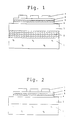
- Fig. 1 depicts a cross-sectional structure illustrating an organic light emitting device in a first embodiment of the present invention.
- the organic light emitting device has a glass substrate 1.
- the glass substrate 1 has a semi-transparent reflective film 2 which is a laminated TiO 2 film and SiO 2 film.
- TBD triphenyl diamine derivative
- PBD electron injecting layer 6 of oxydiazole derivative
- an electrode 7 of Ag-Mg Ag-Mg.
- the sum of optical distances obtained in terms of products of thicknesses of the transparent conductive film 3, the hole injecting layer 4, the light emitting layer 5, and electron injecting layer 6 multiplied by their respective refractive indexes should be made to coincide with 530 nm which is a peak wavelength at which the aluminum chelate compound makes electroluminescent (EL) light emission. This enables the resonator of present invention to function.
- the hole injecting layer 4 and the electron injecting layer 6 as shown in Fig. 1 is not always needed if high performance characteristics are not required.
- the organic light emitting device can be used without either or both of them. With the omission of these layers, holes are injected into the transparent conductive film 3 from the transparent conductive film and electrons from the metal electrode, thereby completing the organic light emitting device.
- the device should preferably have the hole injecting layer 4 and the electron injecting layer 6 provided therein.
- Reflectance of the semi-transparent reflective film 2 should be selected with respect to performance characteristics of the light emitting layer 5 and application of the device.
- An upper limit of the device is restricted in terms of the energy that a light resonator can store without self-destruction.
- the reflectance is 50 to 99.9 % while transmissivity of the semi-transparent reflective film 2 is 50 to 0.1 %.
- the transmissivity of the light to be fed out cannot be made lower than 0.1 %.
- the reflectance is limited to 99.9 %. If the reflectance is made too low, the light resonator cannot function. If it is lower than 50 %, the spectra width cannot be made sufficiently narrow.
- the above-mentioned aluminum chelate compound used for the light emitting layer 5 may be alternatively replaced by perylene derivative, perinone derivative, naphthalene derivative, coumarin derivative, oxadiazole, bisbensoxazoline, aldazine, pyrazine derivative, distilbenzine derivative, polyphenyl derivative, bisstilanthracene derivative, and chelate metal complex.
- any of the above-mentioned organic thin films can be formed by way of evaporation, coating, growing by chemical reaction, the Langmuir project method, or similar techniques.
- the thin films also can be formed of adequate mixtures of a plurality of organic materials.
- Fig. 2 depicts a cross-sectional structure illustrating a previous organic electroluminescent (EL) light emitting device. This previous device is formed with the semi-transparent reflective film 2 removed from the structure shown in Fig 1.
- EL organic electroluminescent
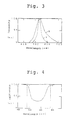
- Fig. 3 depicts a comparison graph illustrating light emission spectra of the devices in Figs. 1 and 2.
- a spectra curve A of the device of the present invention in Fig. 1 has narrower half-width than the previous device in Fig. 2.
- the semi-transparent reflective film 2 makes resonance of light emission in the device to generate an electromagnetic wave of a resonant frequency selectively.
- Such a light emission resonance provides effects that make narrow the half-width of the light emission spectra, increase light emission efficiency, and generate coherent light.
- the effects can be further increased by making the optical distance of a resonating portion of the resonator rather close to the light emission wavelength.
- Fig. 4 depicts a graph illustrating a curve of the half-width of the light emission spectra with respect to the resonating portion of the resonator.
- the curve is the results obtained by a measurement of the device with only a thickness of the hole injecting layer 4 changed in the device structure in Fig. 1.
- the half-width without the semi-transparent reflective film 2 is 100 %.
- the half-width is least around 530 nm at which the optical distance coincides with the peak wavelength, and becomes wide quickly as the wavelength is apart from 530 nm.
- the device having no semi-transparent reflective film 2 has wavelengths of 480 and 580 nm when the light emission intensity is a half of that at 530 nm. This range corresponds to the one in which the half-width in Fig. 4 is made narrow.
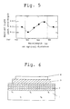
- Fig. 5 depicts a graph illustrating a curve of the optical distance of the resonator with respect to the peak wavelength of the light emitted out of the device having the semi-transparent reflective film 2.
- the resonance provides the phenomenon that if the optical distance is deviated from 530 nm, the peak wavelength of the emitted light also is deviated from 530 nm. If the deviation is too large to cause light emission due to resonance, the peak of the whole light emission becomes close to the peak wavelength of 530 nm when the semi-transparent reflective film 2 is not provided.
- the aluminum chelate used as the material for the light emitting layer in the first embodiment may be alternatively replaced by not only compounds similar to that, but also any of mixtures, laminated layers, and similar organic materials that can emit light by way of electron-hole coupling.
- the device should have an arrangement to keep the device temperature constant to stabilize the resonated light emission.
- Optimum transmissivity and reflectance may vary depending on the device structure and the material forming the semi-transparent reflective film 2, but the absorptance should be preferably as close as to 0.
- the semi-transparent reflective film 2 may be a totally metal reflective film having patterning processed and having a window open for passing light out. Also, the device structure make it hard for light to leak laterally to increase the light emission characteristics further.
- embodiment 1 has the optical distance as resonator made to equal to the light emission wavelength.
- the embodiment also, can theoretically provide similar effects of resonance if the optical distance is times of integers, such as two times, three times, ..., n times the light emission wavelength, and if the optical distance is times of half-integers, such as 1/2 times, 3/2 times, ..., n/2 times the light emission wavelength.
- this embodiment has the total light phase shift made 0 or 1 wavelength by reflections on the upper and lower mirror surfaces.
- the embodiment also, can make resonance for devices having the light shifted 1/2 wavelength on the metal electrode surface and not shifted on the semi-transparent reflecting mirror if the optical length is made 1/4, 3/4, 5/4, and so on, times the light emission wavelength.
- the device of structure in this embodiment makes use of field light emission by electric charge injection and also, can be modified to have a transparent substrate plate to irradiate a light to make the light emitting layer generate a fluorescent light, thereby producing spectra of light emission of narrow half-width similar to that of the field light emission.
- a transparent substrate plate to irradiate a light to make the light emitting layer generate a fluorescent light, thereby producing spectra of light emission of narrow half-width similar to that of the field light emission.
- the organic light emitting devices of the present invention provide such effects as increasing the light emitting characteristics, including making narrow the half-width of light emission spectra, increasing the light emission efficiency, and generating coherent light.
- the organic light emitting devices of the present invention can replace the previous light emitting diodes and semiconductor lasers formed of GaAs, SiC, ZnSe, and similar inorganic semiconductors. They are available for optical communication devices, information display panels, reading/writing heads for optical record file, and optical heads for laser printer.
Landscapes
- Physics & Mathematics (AREA)
- Optics & Photonics (AREA)
- Electroluminescent Light Sources (AREA)
- Luminescent Compositions (AREA)
- Facsimile Heads (AREA)
- Led Devices (AREA)
Claims (14)
- Organische lichtemittierende Vorrichtung mit einem transparenten Substrat (1), einer darauf angeordneten halbtransparenten reflektierenden Schicht (2), einer auf dieser angeordneten und als erste Elektrode dienenden transparenten leitfähigen Schicht (3), einer darauf angeordneten lichtemittierenden Schicht (5) in Form eines dünnen organischen Films und einer auf diesem angeordneten, als reflektierender Spiegel dienenden zweiten Elektrode (7), wobei die halbtransparente reflektierende Schicht das von der lichtemittierenden Schicht emittierte Licht teilweise an das transparente Substrat durchläßt und teilweise auf die lichtemittierende Schicht reflektiert, und wobei die halbtransparente reflektierende Schicht und die auf der lichtemittierenden Schicht angeordnete zweite Elektrode so angeordnet sind, daß sie miteinander als optischer Resonator wirken.
- Organische lichtemittierende Vorrichtung nach Anspruch 1 mit ferner einer zwischen der transparenten leitfähigen Schicht (3) und der lichtemittierenden Schicht (5) angeordneten Löcher injizierenden Schicht (4) und einer zwischen der lichternittierenden Schicht (5) und der zweiten Elektrode (7) angeordneten Elektronen injizierenden Schicht (6).
- Organische lichtemittierende Vorrichtung nach Anspruch 2, wobei die Summe der optischen Wege der transparenten leitfähigen Schicht (3), der Löcher injizierenden Schicht (4), der lichtemittierenden Schicht (5) und der Elektronen injizierenden Schicht (5), jeweils gegeben durch die betreffende, mit dem betreffenden Brechungsindex multiplizierte Dicke, im Bereich des 0,9- bis 1,1-fachen des Wellenlängenmaximums des von der Vorrichtung emittierten Lichtes liegt.
- Organische lichtemittierende Vorrichtung nach Anspruch 1 mit ferner einer zwischen der transparenten leitfahigen Schicht (3) und der lichtemittierenden Schicht (5) angeordneten Löcher injizierenden Schicht (4).
- Organische lichtemittierende Vorrichtung nach Anspruch 1 mit ferner einer zwischen der lichtemittierenden Schicht (5) und der zweiten Elektrode (7) angeordneten Elektronen injizierenden Schicht (6).
- Organische lichtemittierende Vorrichtung nach einem der Ansprüche 1 bis 5, wobei der optische Weg L zwischen der halbtransparenten reflektierenden Schicht (2) und der auf der lichtemittierenden Schicht angeordneten zweiten Elektrode (7) unter der Voraussetzung, daß S < 2L < T ist, durchA die Phasenverschiebung des reflektierten Lichts zwischen der halbtransparenten reflektierten Schicht und der zweiten Elektrode im Bogenmaß ist,P das Wellenlängenmaximum des von der Vorrichtung emittierten Lichts, undS und T diejenigen Wellenlängen sind, bei denen in einem Lichtemissionsspektrum einer lichtemittierenden Vorrichtung, die keine halbtransparente reflektierende Schicht aufweist, die Intensität des emittierten Lichts die Hälfte des Intensitätsmaximums des emittierten Lichts beträgt.
- Organische lichtemittierende Vorrichtung nach einem der Ansprüche 1 bis 5, wobei der optische Weg L zwischen der halbtransparenten reflektierenden Schicht (2) und der auf der lichtemittierenden Schicht angeordneten zweiten Elektrode (7) durchn eine positive ganze Zahl undP das Wellenlängenmaximum des von der Vorrichtung emittierten Lichts ist.
- Organische lichtemittierende Vorrichtung nach einem der Ansprüche 1 bis 5, wobei der optische Weg L zwischen der halbtransparenten reflektierenden Schicht (2) und der auf der lichtemittierenden Schicht angeordneten zweiten Elektrode (7) durchA die Phasenverschiebung des reflektierten Lichts zwischen der halbtransparenten reflektierenden Schicht und der zweiten Elektrode im Bogenmaß undP das Wellenlängenmaximum des von der Vorrichtung emittierten Lichts ist.
- Organische lichtemittierende Vorrichtung nach einem der Ansprüche 1 bis 8, wobei die halbtransparente reflektierende Schicht (2) aus mehreren Schichten aus dielektrischem Material besteht.
- Organische lichtemittierende Vorrichtung nach einem der Ansprüche 1 bis 8, wobei die halbtransparente reflektierende Schicht (2) aus einem total-reflektierenden Metallfilm mit einem Fenster besteht, durch das das Licht nach außen tritt.
- Organische lichtemittierende Vorrichtung nach einem der Ansprüche 1 bis 9, wobei das Reflexionsvermögen der halbtransparenten reflektierenden Schicht (2) 50 bis 99,9% bzw. ihr Transmissionsvermögen 50 bis 0,1% beträgt.
- Zur Herstellung einer organischen lichternittierenden Vorrichtung nach einem der Ansprüche 1 bis 11 geeignete Substratplatte mit einer transparenten Substratplatte (1), einer darauf angeordneten halbtransparenten reflektierenden Schicht (2), die aus mehreren Filmen aus dielektrischem Material besteht und Licht teilweise zu transmittieren und teilweise zu reflektieren vermag, und einer auf der halbtransparenten reflektierenden Schicht ausgebildeten und als Elektrode dienenden transparenten leitfähigen Schicht (3).
- Substratplatte nach Anspruch 12, wobei das Reflexionsvermögen der halbtransparenten reflektierenden Schicht (2) 50 bis 99,9% bzw. ihr Transmissionsvermögen 50 bis 0,1% beträgt.
- Substratplatte nach Anspruch 12 oder 13, wobei die transparente Substratplatte (1) aus Quarz, Glas oder Kunststoff besteht und die transparente leitfähige Schicht (3) auf der halbtransparenten reflektierenden Schicht (2) musterartig ausgebildet ist.
Applications Claiming Priority (5)
| Application Number | Priority Date | Filing Date | Title |
|---|---|---|---|
| JP25252692 | 1992-09-22 | ||
| JP252526/92 | 1992-09-22 | ||
| JP5914593A JP3274527B2 (ja) | 1992-09-22 | 1993-03-18 | 有機発光素子とその基板 |
| JP59145/93 | 1993-03-18 | ||
| PCT/JP1993/001342 WO1994007344A1 (en) | 1992-09-22 | 1993-09-20 | Organic luminescent element and its substrate |
Publications (3)
| Publication Number | Publication Date |
|---|---|
| EP0615401A1 EP0615401A1 (de) | 1994-09-14 |
| EP0615401A4 EP0615401A4 (de) | 1994-11-02 |
| EP0615401B1 true EP0615401B1 (de) | 1999-01-20 |
Family
ID=26400192
Family Applications (1)
| Application Number | Title | Priority Date | Filing Date |
|---|---|---|---|
| EP93919684A Expired - Lifetime EP0615401B1 (de) | 1992-09-22 | 1993-09-20 | Organisches lumineszentes element und sein substrat |
Country Status (5)
| Country | Link |
|---|---|
| US (1) | US5847506A (de) |
| EP (1) | EP0615401B1 (de) |
| JP (1) | JP3274527B2 (de) |
| DE (1) | DE69323176T2 (de) |
| WO (1) | WO1994007344A1 (de) |
Cited By (1)
| Publication number | Priority date | Publication date | Assignee | Title |
|---|---|---|---|---|
| WO2005074330A1 (en) * | 2004-01-28 | 2005-08-11 | Agency For Science, Technology And Research | Multicolor organic light emitting devices |
Families Citing this family (71)
| Publication number | Priority date | Publication date | Assignee | Title |
|---|---|---|---|---|
| JPH07211458A (ja) * | 1994-01-17 | 1995-08-11 | Fuji Electric Co Ltd | 薄膜発光素子 |
| US5780174A (en) * | 1995-10-27 | 1998-07-14 | Kabushiki Kaisha Toyota Chuo Kenkyusho | Micro-optical resonator type organic electroluminescent device |
| JPH09245966A (ja) * | 1996-03-04 | 1997-09-19 | Matsushita Electric Ind Co Ltd | 光透過性反射層を有するelランプおよびその製造方法 |
| US6211613B1 (en) | 1996-04-10 | 2001-04-03 | Cambridge Display Technology Limited | High contrast electroluminescent displays |
| EP0814642A1 (de) * | 1996-06-22 | 1997-12-29 | Ultra Silicon Technology (UK) Limited | Wirkungsverbesserung der elektrolumineszierende Anodnungen |
| KR100741690B1 (ko) * | 1996-09-24 | 2007-07-23 | 세이코 엡슨 가부시키가이샤 | 투사표시장치 및 광원장치 |
| US5869929A (en) * | 1997-02-04 | 1999-02-09 | Idemitsu Kosan Co., Ltd. | Multicolor luminescent device |
| JPH1167448A (ja) | 1997-08-26 | 1999-03-09 | Toyota Central Res & Dev Lab Inc | ディスプレイ装置 |
| JPH11199864A (ja) * | 1997-10-10 | 1999-07-27 | Koto Gijutsu Kenkyuin Kenkyu Kumiai | 電気発光素子の製造方法 |
| JPH11288786A (ja) | 1998-02-04 | 1999-10-19 | Toyota Central Res & Dev Lab Inc | 光共振型有機エレクトロルミネッセンス素子 |
| US6392338B1 (en) | 1998-04-23 | 2002-05-21 | Matsushita Electrical Industrial Co., Ltd. | Organic light emitter having optical waveguide for propagating light along the surface of the substrate |
| US6140764A (en) * | 1998-07-20 | 2000-10-31 | Motorola, Inc. | Organic electroluminescent apparatus with mircrocavity |
| WO2000015009A1 (en) * | 1998-09-02 | 2000-03-16 | Seiko Epson Corporation | Light source and display device |
| JP2000323279A (ja) * | 1999-03-10 | 2000-11-24 | Fuji Photo Film Co Ltd | 露光光源用有機発光素子 |
| GB2349979A (en) * | 1999-05-10 | 2000-11-15 | Cambridge Display Tech Ltd | Light-emitting devices |
| US6411019B1 (en) * | 1999-07-27 | 2002-06-25 | Luxell Technologies Inc. | Organic electroluminescent device |
| GB2353400B (en) * | 1999-08-20 | 2004-01-14 | Cambridge Display Tech Ltd | Mutiple-wavelength light emitting device and electronic apparatus |
| JP4174989B2 (ja) | 1999-11-22 | 2008-11-05 | ソニー株式会社 | 表示装置 |
| GB0008378D0 (en) * | 2000-04-06 | 2000-05-24 | Queen Mary & Westfield College | Light-emitting systems |
| JP3936151B2 (ja) * | 2000-05-08 | 2007-06-27 | 双葉電子工業株式会社 | 有機el素子 |
| JP2002110344A (ja) * | 2000-09-29 | 2002-04-12 | Tdk Corp | 薄膜el素子及びその製造方法 |
| JP2002252088A (ja) * | 2001-02-27 | 2002-09-06 | Nec Corp | 発光体、発光素子部、およびそれを用いた発光表示装置 |
| EP1296384B1 (de) * | 2001-09-21 | 2008-09-03 | FUJIFILM Corporation | Organische elektrolumineszente Vorrichtung |
| JP2003109775A (ja) * | 2001-09-28 | 2003-04-11 | Sony Corp | 有機電界発光素子 |
| JP4023655B2 (ja) | 2001-11-07 | 2007-12-19 | 双葉電子工業株式会社 | 透明膜状乾燥剤及び透明液状乾燥剤 |
| US7514158B2 (en) * | 2001-12-13 | 2009-04-07 | Kabushiki Kaisha Hayashibara Seibutsu Kagaku Kenkyujo | Coumarin compound |
| CA2419121A1 (en) * | 2002-05-03 | 2003-11-03 | Luxell Technologies, Inc. | Dark layer for an electroluminescent device |
| CN1666579A (zh) * | 2002-05-08 | 2005-09-07 | 泽奥勒克斯公司 | 使用反馈增强型发光二极管的照明器件 |
| US6946790B2 (en) * | 2002-10-08 | 2005-09-20 | Pioneer Corporation | Organic electroluminescence device |
| DE10301029B4 (de) * | 2003-01-13 | 2005-03-17 | Ritter Gmbh | Kartuschenverschluß mit Öffnungs-/Schließ-Funktion |
| US6861800B2 (en) * | 2003-02-18 | 2005-03-01 | Eastman Kodak Company | Tuned microcavity color OLED display |
| JP2004355813A (ja) * | 2003-05-27 | 2004-12-16 | Tohoku Pioneer Corp | 自発光表示装置およびこれを用いた情報機器 |
| US6790696B1 (en) * | 2003-06-30 | 2004-09-14 | Eastman Kodak Company | Providing an organic vertical cavity laser array device with etched region in dielectric stack |
| US7321197B2 (en) | 2003-08-27 | 2008-01-22 | Hitachi Displays, Ltd. | High-efficiency organic light emitting element |
| US7973319B2 (en) | 2003-09-19 | 2011-07-05 | Sony Corporation | Display unit, method of manufacturing same, organic light emitting unit, and method of manufacturing same |
| JP4428979B2 (ja) * | 2003-09-30 | 2010-03-10 | 三洋電機株式会社 | 有機elパネル |
| JP4497881B2 (ja) * | 2003-09-30 | 2010-07-07 | 三洋電機株式会社 | 有機el素子および有機elパネル |
| JP4716699B2 (ja) | 2003-09-30 | 2011-07-06 | 三洋電機株式会社 | 有機elパネル |
| US7268485B2 (en) * | 2003-10-07 | 2007-09-11 | Eastman Kodak Company | White-emitting microcavity OLED device |
| KR100563058B1 (ko) * | 2003-11-21 | 2006-03-24 | 삼성에스디아이 주식회사 | 유기 전계 발광 소자 |
| JP4475942B2 (ja) | 2003-12-26 | 2010-06-09 | 三洋電機株式会社 | 表示装置及びその製造方法 |
| JP4439260B2 (ja) | 2003-12-26 | 2010-03-24 | 三洋電機株式会社 | 表示装置の製造方法 |
| KR100704258B1 (ko) * | 2004-06-02 | 2007-04-06 | 세이코 엡슨 가부시키가이샤 | 유기 el 장치 및 전자 기기 |
| US7196469B2 (en) * | 2004-06-18 | 2007-03-27 | Eastman Kodak Company | Reducing undesirable absorption in a microcavity OLED |
| KR100683693B1 (ko) | 2004-11-10 | 2007-02-15 | 삼성에스디아이 주식회사 | 발광 장치 |
| WO2006073908A2 (en) * | 2004-12-30 | 2006-07-13 | E.I. Dupont De Nemours And Company | Electronic device having a mirror stack |
| JP4210690B2 (ja) * | 2006-03-31 | 2009-01-21 | Dowaエレクトロニクス株式会社 | 面発光素子 |
| US7622865B2 (en) * | 2006-06-19 | 2009-11-24 | Seiko Epson Corporation | Light-emitting device, image forming apparatus, display device, and electronic apparatus |
| JP4899929B2 (ja) * | 2007-02-28 | 2012-03-21 | セイコーエプソン株式会社 | 表示装置 |
| JP2008226718A (ja) * | 2007-03-14 | 2008-09-25 | Fuji Electric Holdings Co Ltd | 有機el素子 |
| KR100813850B1 (ko) * | 2007-03-29 | 2008-03-17 | 삼성에스디아이 주식회사 | 발광 장치 |
| JP2009205928A (ja) | 2008-02-27 | 2009-09-10 | Fuji Electric Holdings Co Ltd | 微小共振器色変換el素子およびそれを用いた有機elディスプレイ |
| JP4843627B2 (ja) * | 2008-03-07 | 2011-12-21 | 株式会社 日立ディスプレイズ | 有機発光素子 |
| KR100909389B1 (ko) | 2008-04-21 | 2009-07-24 | 삼성모바일디스플레이주식회사 | 유기전계발광표시장치 |
| KR100953658B1 (ko) | 2008-06-05 | 2010-04-20 | 삼성모바일디스플레이주식회사 | 유기전계발광 표시장치 |
| JP5288966B2 (ja) | 2008-09-22 | 2013-09-11 | ユー・ディー・シー アイルランド リミテッド | 発光素子及びその製造方法、並びに該発光素子を備えるディスプレイ |
| JP2010153820A (ja) | 2008-11-21 | 2010-07-08 | Fujifilm Corp | 有機電界発光素子 |
| JP5127814B2 (ja) * | 2008-12-19 | 2013-01-23 | キヤノン株式会社 | 有機発光素子及びそれを利用した発光装置、表示装置 |
| JP5164825B2 (ja) | 2008-12-19 | 2013-03-21 | キヤノン株式会社 | 有機発光素子 |
| US20110058770A1 (en) * | 2009-09-10 | 2011-03-10 | E. I. Du Pont De Nemours And Company | Sub-surface engraving of oled substrates for improved optical outcoupling |
| JP5676867B2 (ja) | 2009-09-29 | 2015-02-25 | 住友化学株式会社 | 有機エレクトロルミネッセンス素子 |
| KR20110040308A (ko) * | 2009-10-14 | 2011-04-20 | 순천향대학교 산학협력단 | 발광 소자, 이를 구비하는 표시 장치 및 조명 유닛 |
| JP5404709B2 (ja) * | 2011-08-02 | 2014-02-05 | 株式会社沖データ | 半導体装置、led装置、ledヘッド、及び画像形成装置 |
| US9017794B1 (en) * | 2011-11-21 | 2015-04-28 | The United States Of America As Represented By The Secretary Of The Navy | Integrated plasmonic enhanced fluorescence for sensor application |
| TWI661587B (zh) * | 2012-10-11 | 2019-06-01 | The Regents Of The University Of Michigan | 發電彩色塗料 |
| JP6111643B2 (ja) | 2012-12-17 | 2017-04-12 | セイコーエプソン株式会社 | 有機エレクトロルミネッセンス装置、及び電子機器 |
| JP6488082B2 (ja) * | 2013-12-02 | 2019-03-20 | 株式会社半導体エネルギー研究所 | 発光装置、電子機器、および照明装置 |
| KR102231631B1 (ko) * | 2014-10-08 | 2021-03-24 | 삼성디스플레이 주식회사 | 유기 발광 표시 장치 |
| CN107409458A (zh) * | 2015-03-09 | 2017-11-28 | Beneq有限公司 | 显示设备及用于制造这样的设备的方法 |
| JP6695785B2 (ja) * | 2016-11-29 | 2020-05-20 | 株式会社Joled | 発光装置、表示装置および照明装置 |
| JP7237536B2 (ja) | 2018-11-12 | 2023-03-13 | 株式会社ジャパンディスプレイ | 表示装置 |
Family Cites Families (12)
| Publication number | Priority date | Publication date | Assignee | Title |
|---|---|---|---|---|
| JPH0824071B2 (ja) * | 1987-11-16 | 1996-03-06 | 日本電信電話株式会社 | 薄膜エレクトロルミネセンス素子 |
| JPH01236672A (ja) * | 1988-03-17 | 1989-09-21 | Seiko Epson Corp | 光双安定素子 |
| JPH0212795A (ja) * | 1988-06-29 | 1990-01-17 | Nec Corp | 有機薄膜el素子とその製造方法 |
| JP2583994B2 (ja) * | 1988-08-05 | 1997-02-19 | 松下電器産業株式会社 | 薄膜エレクトロルミネセンス装置 |
| JP2503605B2 (ja) * | 1988-09-13 | 1996-06-05 | 日本電気株式会社 | 赤外線センサ |
| JPH0278280A (ja) * | 1988-09-14 | 1990-03-19 | Ricoh Co Ltd | 半導体発光装置 |
| JP2879080B2 (ja) * | 1989-03-23 | 1999-04-05 | 株式会社リコー | 電界発光素子 |
| JPH0733433Y2 (ja) * | 1989-11-10 | 1995-07-31 | トヨタ自動車株式会社 | 薄膜el素子 |
| JPH03186187A (ja) * | 1989-12-15 | 1991-08-14 | Nkk Corp | 電気炉のスパウト補修方法 |
| JP2689661B2 (ja) * | 1989-12-18 | 1997-12-10 | 松下電器産業株式会社 | 光干渉フィルタを含む薄膜エレクトロルミネセンス装置 |
| JP2829107B2 (ja) * | 1990-08-29 | 1998-11-25 | 株式会社東芝 | 有機薄膜el素子 |
| JP2846483B2 (ja) * | 1991-01-18 | 1999-01-13 | 出光興産株式会社 | 有機エレクトロルミネッセンス素子及びその製造方法 |
-
1993
- 1993-03-18 JP JP5914593A patent/JP3274527B2/ja not_active Expired - Lifetime
- 1993-09-20 EP EP93919684A patent/EP0615401B1/de not_active Expired - Lifetime
- 1993-09-20 DE DE69323176T patent/DE69323176T2/de not_active Expired - Lifetime
- 1993-09-20 WO PCT/JP1993/001342 patent/WO1994007344A1/ja not_active Ceased
-
1995
- 1995-10-23 US US08/546,913 patent/US5847506A/en not_active Expired - Lifetime
Cited By (1)
| Publication number | Priority date | Publication date | Assignee | Title |
|---|---|---|---|---|
| WO2005074330A1 (en) * | 2004-01-28 | 2005-08-11 | Agency For Science, Technology And Research | Multicolor organic light emitting devices |
Also Published As
| Publication number | Publication date |
|---|---|
| JP3274527B2 (ja) | 2002-04-15 |
| US5847506A (en) | 1998-12-08 |
| JPH08213174A (ja) | 1996-08-20 |
| DE69323176D1 (de) | 1999-03-04 |
| DE69323176T2 (de) | 1999-09-02 |
| WO1994007344A1 (en) | 1994-03-31 |
| EP0615401A4 (de) | 1994-11-02 |
| EP0615401A1 (de) | 1994-09-14 |
Similar Documents
| Publication | Publication Date | Title |
|---|---|---|
| EP0615401B1 (de) | Organisches lumineszentes element und sein substrat | |
| US5554911A (en) | Light-emitting elements | |
| EP0654833B1 (de) | Gegenstand, der Lichtquellen mit Resonator enthält | |
| US7292614B2 (en) | Organic laser and liquid crystal display | |
| EP0683623B1 (de) | Gegenstand mit Mikrohohlraum-Lichtquelle | |
| US5932895A (en) | Saturated full color stacked organic light emitting devices | |
| US6396860B1 (en) | Organic semiconductor laser | |
| US7965037B2 (en) | Organic electroluminescence device and organic laser diode | |
| US6160828A (en) | Organic vertical-cavity surface-emitting laser | |
| KR100852067B1 (ko) | 레이저 방출 장치 | |
| JP4289512B2 (ja) | 有機レーザー | |
| US8059692B2 (en) | Laser oscillator | |
| US6330262B1 (en) | Organic semiconductor lasers | |
| JPH10177896A (ja) | 有機発光素子 | |
| US7449724B2 (en) | Light-emitting device | |
| KR20050056875A (ko) | 전계발광 디바이스 | |
| US20050069012A1 (en) | Light emitting device | |
| Becker et al. | Light emission from wavelength-tunable microcavities | |
| JP2830474B2 (ja) | 有機発光素子とその基板 | |
| US7522644B2 (en) | Laser oscillator | |
| JPWO1994007344A1 (ja) | 有機発光素子とその基板 | |
| Guss et al. | Microresonator effects in optically and electrically pumped thin-film light-emitting diodes | |
| US20240397749A1 (en) | Band-edge emission enhanced organic light emitting diodes with simplified structures and high energy efficiency | |
| Fujii et al. | Novel characteristics of electroluminescent diode with organic superlattice structure utilizing 8-hydroxyquinoline aluminum and aromatic diamine | |
| Auffray et al. | 61‐3: Distinguished Paper: Realization of an Organic Semiconductor Electroluminescent Device with High Directionality and Color Purity |
Legal Events
| Date | Code | Title | Description |
|---|---|---|---|
| PUAI | Public reference made under article 153(3) epc to a published international application that has entered the european phase |
Free format text: ORIGINAL CODE: 0009012 |
|
| 17P | Request for examination filed |
Effective date: 19940615 |
|
| AK | Designated contracting states |
Kind code of ref document: A1 Designated state(s): DE GB NL |
|
| A4 | Supplementary search report drawn up and despatched | ||
| AK | Designated contracting states |
Kind code of ref document: A4 Designated state(s): DE FR GB NL |
|
| 17Q | First examination report despatched |
Effective date: 19961205 |
|
| GRAG | Despatch of communication of intention to grant |
Free format text: ORIGINAL CODE: EPIDOS AGRA |
|
| GRAG | Despatch of communication of intention to grant |
Free format text: ORIGINAL CODE: EPIDOS AGRA |
|
| GRAH | Despatch of communication of intention to grant a patent |
Free format text: ORIGINAL CODE: EPIDOS IGRA |
|
| RAP1 | Party data changed (applicant data changed or rights of an application transferred) |
Owner name: KAKUTA, ATSUSHI Owner name: ITO, YUZO Owner name: HATTORI, SHINTARO Owner name: NAKAYAMA, TAKAHIRO Owner name: HITACHI, LTD. |
|
| RAP1 | Party data changed (applicant data changed or rights of an application transferred) |
Owner name: HITACHI, LTD. |
|
| GRAH | Despatch of communication of intention to grant a patent |
Free format text: ORIGINAL CODE: EPIDOS IGRA |
|
| RBV | Designated contracting states (corrected) |
Designated state(s): DE GB NL |
|
| GRAA | (expected) grant |
Free format text: ORIGINAL CODE: 0009210 |
|
| AK | Designated contracting states |
Kind code of ref document: B1 Designated state(s): DE GB NL |
|
| REF | Corresponds to: |
Ref document number: 69323176 Country of ref document: DE Date of ref document: 19990304 |
|
| PG25 | Lapsed in a contracting state [announced via postgrant information from national office to epo] |
Ref country code: DE Free format text: LAPSE BECAUSE OF FAILURE TO SUBMIT A TRANSLATION OF THE DESCRIPTION OR TO PAY THE FEE WITHIN THE PRESCRIBED TIME-LIMIT Effective date: 19990421 |
|
| PLBE | No opposition filed within time limit |
Free format text: ORIGINAL CODE: 0009261 |
|
| STAA | Information on the status of an ep patent application or granted ep patent |
Free format text: STATUS: NO OPPOSITION FILED WITHIN TIME LIMIT |
|
| 26N | No opposition filed | ||
| REG | Reference to a national code |
Ref country code: GB Ref legal event code: IF02 |
|
| PGFP | Annual fee paid to national office [announced via postgrant information from national office to epo] |
Ref country code: GB Payment date: 20120919 Year of fee payment: 20 |
|
| PGFP | Annual fee paid to national office [announced via postgrant information from national office to epo] |
Ref country code: DE Payment date: 20120912 Year of fee payment: 20 |
|
| PGFP | Annual fee paid to national office [announced via postgrant information from national office to epo] |
Ref country code: NL Payment date: 20120919 Year of fee payment: 20 |
|
| REG | Reference to a national code |
Ref country code: DE Ref legal event code: R071 Ref document number: 69323176 Country of ref document: DE |
|
| REG | Reference to a national code |
Ref country code: DE Ref legal event code: R071 Ref document number: 69323176 Country of ref document: DE |
|
| REG | Reference to a national code |
Ref country code: NL Ref legal event code: V4 Effective date: 20130920 |
|
| REG | Reference to a national code |
Ref country code: GB Ref legal event code: PE20 Expiry date: 20130919 |
|
| PG25 | Lapsed in a contracting state [announced via postgrant information from national office to epo] |
Ref country code: DE Free format text: LAPSE BECAUSE OF EXPIRATION OF PROTECTION Effective date: 20130921 |
|
| PG25 | Lapsed in a contracting state [announced via postgrant information from national office to epo] |
Ref country code: GB Free format text: LAPSE BECAUSE OF EXPIRATION OF PROTECTION Effective date: 20130919 |