EP0616416B1 - Dispositif de conversion - Google Patents
Dispositif de conversion Download PDFInfo
- Publication number
- EP0616416B1 EP0616416B1 EP93309892A EP93309892A EP0616416B1 EP 0616416 B1 EP0616416 B1 EP 0616416B1 EP 93309892 A EP93309892 A EP 93309892A EP 93309892 A EP93309892 A EP 93309892A EP 0616416 B1 EP0616416 B1 EP 0616416B1
- Authority
- EP
- European Patent Office
- Prior art keywords
- current
- circuit
- conversion apparatus
- reactor
- prescribed value
- Prior art date
- Legal status (The legal status is an assumption and is not a legal conclusion. Google has not performed a legal analysis and makes no representation as to the accuracy of the status listed.)
- Expired - Lifetime
Links
- 238000006243 chemical reaction Methods 0.000 title claims description 45
- 238000004804 winding Methods 0.000 claims description 11
- 239000003990 capacitor Substances 0.000 claims description 6
- 230000007257 malfunction Effects 0.000 claims description 6
- 230000001105 regulatory effect Effects 0.000 claims 4
- 230000001276 controlling effect Effects 0.000 claims 2
- 238000010586 diagram Methods 0.000 description 9
- 229920006395 saturated elastomer Polymers 0.000 description 6
- 230000000694 effects Effects 0.000 description 3
- 238000000034 method Methods 0.000 description 2
- 230000001681 protective effect Effects 0.000 description 2
- 230000015556 catabolic process Effects 0.000 description 1
- 239000002131 composite material Substances 0.000 description 1
- 238000010276 construction Methods 0.000 description 1
- 238000001514 detection method Methods 0.000 description 1
- 239000004065 semiconductor Substances 0.000 description 1
Images

Classifications
-
- H—ELECTRICITY
- H02—GENERATION; CONVERSION OR DISTRIBUTION OF ELECTRIC POWER
- H02H—EMERGENCY PROTECTIVE CIRCUIT ARRANGEMENTS
- H02H7/00—Emergency protective circuit arrangements specially adapted for specific types of electric machines or apparatus or for sectionalised protection of cable or line systems, and effecting automatic switching in the event of an undesired change from normal working conditions
- H02H7/10—Emergency protective circuit arrangements specially adapted for specific types of electric machines or apparatus or for sectionalised protection of cable or line systems, and effecting automatic switching in the event of an undesired change from normal working conditions for converters; for rectifiers
- H02H7/12—Emergency protective circuit arrangements specially adapted for specific types of electric machines or apparatus or for sectionalised protection of cable or line systems, and effecting automatic switching in the event of an undesired change from normal working conditions for converters; for rectifiers for static converters or rectifiers
- H02H7/122—Emergency protective circuit arrangements specially adapted for specific types of electric machines or apparatus or for sectionalised protection of cable or line systems, and effecting automatic switching in the event of an undesired change from normal working conditions for converters; for rectifiers for static converters or rectifiers for inverters, i.e. DC/AC converters
- H02H7/1225—Emergency protective circuit arrangements specially adapted for specific types of electric machines or apparatus or for sectionalised protection of cable or line systems, and effecting automatic switching in the event of an undesired change from normal working conditions for converters; for rectifiers for static converters or rectifiers for inverters, i.e. DC/AC converters responsive to internal faults, e.g. shoot-through
-
- G—PHYSICS
- G05—CONTROLLING; REGULATING
- G05F—SYSTEMS FOR REGULATING ELECTRIC OR MAGNETIC VARIABLES
- G05F1/00—Automatic systems in which deviations of an electric quantity from one or more predetermined values are detected at the output of the system and fed back to a device within the system to restore the detected quantity to its predetermined value or values, i.e. retroactive systems
- G05F1/10—Regulating voltage or current
- G05F1/46—Regulating voltage or current wherein the variable actually regulated by the final control device is DC
- G05F1/56—Regulating voltage or current wherein the variable actually regulated by the final control device is DC using semiconductor devices in series with the load as final control devices
- G05F1/565—Regulating voltage or current wherein the variable actually regulated by the final control device is DC using semiconductor devices in series with the load as final control devices sensing a condition of the system or its load in addition to means responsive to deviations in the output of the system, e.g. current, voltage, power factor
- G05F1/569—Regulating voltage or current wherein the variable actually regulated by the final control device is DC using semiconductor devices in series with the load as final control devices sensing a condition of the system or its load in addition to means responsive to deviations in the output of the system, e.g. current, voltage, power factor for protection
- G05F1/573—Regulating voltage or current wherein the variable actually regulated by the final control device is DC using semiconductor devices in series with the load as final control devices sensing a condition of the system or its load in addition to means responsive to deviations in the output of the system, e.g. current, voltage, power factor for protection with overcurrent detector
-
- H—ELECTRICITY
- H02—GENERATION; CONVERSION OR DISTRIBUTION OF ELECTRIC POWER
- H02M—APPARATUS FOR CONVERSION BETWEEN AC AND AC, BETWEEN AC AND DC, OR BETWEEN DC AND DC, AND FOR USE WITH MAINS OR SIMILAR POWER SUPPLY SYSTEMS; CONVERSION OF DC OR AC INPUT POWER INTO SURGE OUTPUT POWER; CONTROL OR REGULATION THEREOF
- H02M7/00—Conversion of AC power input into DC power output; Conversion of DC power input into AC power output
- H02M7/42—Conversion of DC power input into AC power output without possibility of reversal
- H02M7/44—Conversion of DC power input into AC power output without possibility of reversal by static converters
- H02M7/48—Conversion of DC power input into AC power output without possibility of reversal by static converters using discharge tubes with control electrode or semiconductor devices with control electrode
Definitions
- the present invention relates to a conversion apparatus which uses high-speed switching devices (abbreviated below to HSDs) possessing two functions, latch type and non-latch type functions.
- HSDs high-speed switching devices
- GTO gate turn off
- transistors transistors.
- GTO is a latch type device, which means that once the GTO is brought to an ON state by applying a signal to its gate, anode current continues to flow even if the gate signal is made "0".
- a transistor on the other hand, conducts when a base signal is supplied but the collector current becomes "0" when the base signal is removed.
- a device such as this will be called a non-latch type device here.
- GTOs are widely used as high-voltage, high-current semiconductor devices whose turn-on voltage is comparatively low. But since current filamentation occurs when they are switched OFF, their breakdown withstand capability is low and large snubber circuits are necessary. Also, their switching speed is not fast.
- an insulated gate bipolar transistor (called IGBT below) is not liable to break down, since there is no current filamentation, and its switching speed is fast, but it is not suitable for high-voltage applications.
- IGBT insulated gate bipolar transistor
- a specific example is the device shown in Japanese Laid-open Patent Application No. 64-758.
- FIG. 8 An example of a conventional conversion apparatus using the latch type devices GTOs is disclosed in EP-B-0 105 510.
- 1 is a DC power source
- 2P and 2N are DC circuit breakers
- 3 is a DC reactor
- 4 is a DC capacitor
- 5 is a reactor
- 6 is a diode
- 7 and 8 are DC buses
- 11, 12, 13, 14, 15 and 16 are GTos
- 17, 18, 19, 20, 21 and 22 are feedback diodes
- 25U, 25V and 25W are AC circuit breakers.
- This circuit is widely used and is well-known as ah inverter and, although not shown, snubber circuits and gate circuits, etc. are needed, but a description of the operation of this circuit will be omitted here.
- Overcurrent protection of the devices in a circuit such as this is provided by including elements, usually reactors or fuses, which restrict the magnitude of current to below the surge current withstand capability that can be withstood by the devices themselves.
- the surge current withstand capability is 7000 A in the case of a sinusoidal half wave with a width of 10 ms.
- reactor 5 keeps short-circuit current to a value that is below the surge current withstand capability of GTOs 11 and 12, etc. and DC reactor 3 suppresses inflow of current from the DC power source 1 in the time up to when DC circuit breakers 2 are opened.
- Reactor 5 must be so designed that it does not become saturated by excessive current flowing in during this period.
- DC reactor 3 must be an element that is not saturated by the voltage-time product to which it is subjected during the short circuit period. Consequently, they are both made large reactors.
- AC circuit breakers 25U, 25V and 25W shall be opened immediately when there is inflow of current from loads not shown or when fault circuits and loads are to be isolated.
- non-latch type devices i.e., transistors
- the overcurrent can be stopped immediately by applying reverse bias to their bases if a short circuit occurs.
- Reactor 5 is not absolutely necessary but since it acts to suppress current if it is present, it allows a time delay up to the time of protective action following a short circuit. Since the current at the time of a short circuit is at most about double that of normal operation, even if reactor 5 is included it need only be a small reactor.
- a conversion apparatus comprising:
- a conversion apparatus comprising:
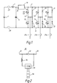
- Fig. 1 is a circuit diagram showing one embodiment of the invention.
- 30 is a non-linear impedance circuit that is described later, and 31 and 32 indicate the main terminal portions of this circuit 30.
- 51 to 56 are HSDs that can change over between latch type and non-latch type functions, and for convenience the symbol used therefor is made a composite symbol of a GTO and a transistor. The way such an HSD is used is that in the ON state a gate selection is made to make it a latch type device and several ⁇ s prior to effecting turn-off operation a gate selection is made to make it a non-latch type device.
- gates are selected depends on the structure of the HSD but possible ways are, for example, to effect turn-on by supplying gate signals simultaneously to a gate G1 for non-latch type device and a gate G2 for latch type device and to effect turn-off by turning the gate signal of gate G1 OFF after turning the gate signal of gate G2 OFF or to make sections by means of the levels of voltages that are supplied to the gates G1 and G2.
- a circuit for generating the above-described gate signals is apparent to those skilled in the art, so that a detailed description of the circuit construction may be omitted.
- Non-linear impedance circuit 30 displays nearly zero impedance when the current flowing through it is less than a value I2 and displays a larger inductance L when this current is equal to or greater than the value I2 but less than a value I3 (I2 ⁇ I3 ⁇ I1). At the value I3 or more, it returns to nearly zero impedance.
- the value I2 is set at about 1/2 of the limit value I1.
- HSD 52 is turned ON in error while HSD 51 is ON, DC buses 7 and 8 are short-circuited and so the charge of DC capacitor 4 tries to discharge through non-linear impedance circuit 30 and HSDs 51 and 52. Since the impedance of non-linear impedance circuit 30 is nearly zero when the discharge current Ic is less than the value I2, the discharge current Ic rises rapidly. But when the current Ic reaches the value I2, the inductance of non-linear impedance circuit 30 changes to L, and so the current increase ratio changes to E/L where E is the DC capacitor 30's charging voltage.
- HSDs 51 and 52 Since, even at its maximum, the value of the current flowing in HSDs 51 and 52 is I2 + (E/L)t, HSDs 51 and 52 and the other HSDs are changed from latch type to non-latch type devices and turned OFF before the value of this current reaches the limit value I1.
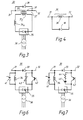
- non-linear impedance circuit 30 is shown in Fig. 2.
- 33 is a high-speed diode
- 34 is a reactor
- 35 is a rectifier
- 36 is a transformer.
- the primary side of transformer 36 is connected to a power supply not shown.
- Diode 33 stops current flowing from main terminal 31 to main terminal 32, but it has no ability to block any current that is less than the value I2 if, because of rectifier 35, DC current with the value I2 flows in the series circuit consisting of diode 33 and inductor 34. That is, seen from the exterior, its impedance is zero.
- Fig. 3 shows another embodiment of non-linear impedance circuit 30.
- a saturable reactor 37 and a diode 38 are used in place of diode 33.
- Saturable reactor 37 is provided with a primary winding 371 and a secondary winding 372.
- the turn ratio of primary winding 371 to secondary winding 372 is 1 to n. Since DC current with the value I2' flows in the secondary winding 372 of saturable inductor 37, saturable reactor 37 is saturated and the impedance between main terminals 31 and 32 is virtually zero.
- saturable reactor 37 goes to an unsaturated state and displays the characteristic of a reactor with an inductance L.
- a reactor 34a is inserted in the circuit in a manner such that the value of its current does not change much because of voltage that is produced when saturable reactor 37 is unsaturated.
- Diode 38 is not absolutely essential, but it acts to absorb the voltage produced by the extremely small inductance that is displayed when saturable reactor 37 is saturated and to reduce the switching surge voltage that is imposed on HSDs 51 - 56 and feedback diodes 17 - 22.
- Fig. 4 shows a further embodiment of non-linear impedance circuit 30.
- Reactor 39 is a special reactor in which a permanent magnet is embedded. Because of the permanent magnet, the reactor's inductance is virtually zero when the current flowing in its coil is less than the value I2, but becomes L when the current reaches the value 12. It is satisfactory that reactor 39 is small enough not to become saturated in the period of several tens of ⁇ s during which a short circuit is detected and the HSDs are changed from latch type to non-latch type devices and a turn-off operation is performed. The role of diode 38 is the same as in Fig. 3.
- Fig. 5 is a circuit of a conversion apparatus in which non-linear impedance circuits 301 - 306 are included individually for respective HSDs 51 - 56.
- the value I2 must be made lower than the limit current value I1 of the HSD. The reason for this is that in the HSDs there is superimposition of the current flowing from the non-linear impedance circuit 30 on the current flowing back through the load, the HSDs and feedback diodes.
- non-linear impedance circuits 301 - 306 are provided individually for respective HSDs 51 - 56 as in Fig.
- non-linear impedance circuit 30 as an element or circuit possessing a current-limiting function for suppressing the rate of current increase as from the time when current flowing through HSDs 51 - 56 exceeds a set value. But, it is also, possible to use an element or circuit that possesses a function of increasing the impedance and restricting current from exceeding a set value or reducing the current to below a set value as from the time when current flowing through HSDs exceeds the set value.
- non-linear impedance circuit 30 is shown in Figs. 6 and 7. Parts which are the same as in Fig. 2 are given the same number and a description thereof is omitted.
- thyristor 41 is a thyristor
- 42 is an IGBT
- 43 is a non-linear resistor.
- this circuit is used with thyristor 41 off and IGBT 42 on, so that it functions the same way as in Fig. 2.
- I2 diode 33 becomes reverse-biased.
- IGBT 42 is turned off and the thyristor 41 is turned on.
- a thyristor rectifier is used as rectifier 35, it is better to delay the phase of triggering thyristors. If thyristor 41 keeps off state, the energy stored in reactor 34 heats non-linear resistor 43 in vain.
- Thyristor 41 is not necessarily provided if non-linear resistor 43 has much heat margin.
- Non-linear resistor 43 is used for overvoltage protection of IGBT 42.
- a resistor, a series circuit of a resistor 44 and a capacitor 45 shown in Fig. 7 or another circuit may be used as far as it can protect IGBT 42.
- non-linear impedance circuit 30 shown in Fig. 6 has a function for increasing the impedance and restricting current from exceeding a set value as from the time when current flowing through HSDs exceeds the set value.
- non-linear impedance circuit 30 has almost the same function as described above.
- Non-linear impedance circuit 30 shown in Fig. 7 has a function for increasing the impedance and reducing the current to below a set value as from the time when current flowing through HSDs exceeds the set value.
- the conversion apparatus of Fig. 1 and Fig. 5 the overcurrent of short circuits, etc. is detected by the method of detecting current in ordinary current transformers, it can also be detected by detecting the voltage produced in the non-linear impedance circuits.
- the non-linear impedance circuits In order that the non-linear impedance circuits are made to be small, they display high impedance at a certain value of current. So, from the point of view of HSD protection, it is preferable not to supply a turn-off signal to an HSD in a state in which the current has reached a value exceeding the level of this certain value.
- a circuit to detect DC short circuit is provided. And, in a control circuit (not shown) of the conversion apparatus, there is provided a circuit to generate signals for turning ON the respective HSD simultaneously based on the detection of the DC short circuit.
- a control circuit not shown
- a circuit to generate signals for turning ON the respective HSD simultaneously based on the detection of the DC short circuit By this circuit all the HSDs in the conversion apparatus are turned on, the risk of damage can be reduced, since the flow of overcurrent is not concentrated in a specific HSD but becomes divided. Further, surer protection is made possible if division of overcurrent is accompanied by interruption of DC breakers 2P and 2N on the input side of the conversion apparatus and, if required, AC circuit breakers 25U, 25V and 25W.
- the reliability of conversion apparatus can be improved, since sure short-circuit protection of the devices is made possible by constituting the conversion apparatus by high-speed switching devices which perform turn-off operations after changing from latch type to non-latch type. Also, the reactors used for suppressing short-circuit current can be made smaller than in the case where latch type devices are used. Further, the power losses generated in conversion apparatus can be made less than in the case where non-latch type devices are used.
Landscapes
- Engineering & Computer Science (AREA)
- Power Engineering (AREA)
- Physics & Mathematics (AREA)
- Electromagnetism (AREA)
- General Physics & Mathematics (AREA)
- Radar, Positioning & Navigation (AREA)
- Automation & Control Theory (AREA)
- Inverter Devices (AREA)
- Power Conversion In General (AREA)
- Rectifiers (AREA)
- Dc-Dc Converters (AREA)
Claims (17)
- Dispositif de conversion comprenant :une pluralité de dispositifs de commutation à grande vitesse (51, 52, 53, 54, 55, 56), susceptibles d'être actionnés chacun en commandant une grille de ceux-ci dans un fonctionnement de type à verrouillage et de type à non verrouillage ;des moyens formant source d'alimentation (1) pour fournir le courant auxdits dispositifs de commutation à grande vitesse, formant de ce fait un chemin de courant desdits dispositifs de commutation à grande vitesse ;lesdits dispositifs de commutation à grande vitesse étant mis à l'état bloqué après la commutation dudit fonctionnement de type à verrouillage vers ledit fonctionnement de type à non verrouillage lorsque ledit courant est inférieur à une valeur limite (I1), caractérisé par :un circuit à impédance non linéaire (30) comprenant une inductance et des éléments contrôlables prévus dans ledit chemin de courant pour limiter ledit courant provenant desdits moyens formant source d'alimentation, par exemple à partir d'un moment où ledit courant atteint une valeur prescrite (I2) inférieure à ladite valeur limite (In) et agencés de sorte que, dans le cas d'une défaillance due à une surintensité de courant, ledit dispositif de commutation à grande vitesse est commuté dudit fonctionnement de type à verrouillage vers ledit fonctionnement de type à non verrouillage et, ensuite, mis à l'état bloqué tandis que lesdits moyens de régulation de courant régulent ledit courant,de telle manière que ledit dispositif de commutation à grande vitesse soit protégé dans le cas d'une défaillance due à une surintensité de courant.
- Dispositif de conversion selon la revendication 1, dans lequel :lesdits moyens de régulation de courant (30) régulent ledit courant de telle sorte que la vitesse d'accroissement dudit courant soit annulée lorsque ledit courant atteint ladite valeur prescrite.
- Dispositif de conversion selon la revendication 2, dans lequel :ladite impédance non linéaire (30) a une impédance sensiblement nulle lorsque ledit courant qui circule à travers lesdits moyens de régulation de courant est inférieur à ladite valeur prescrite et a au moins une composante d'inductance lorsque ledit courant est égal ou supérieur à ladite valeur prescrite.
- Dispositif de conversion selon la revendication 3, dans lequel :ladite impédance non linéaire (30) comprend un circuit qui comprend,une diode à grande vitesse (33), etun réseau série constitué d'une bobine (34) et d'un redresseur (35),ledit réseau série étant connecté en parallèle avec ladite diode à grande vitesse (33),ledit redresseur fournissant un courant continu de ladite valeur prédéterminée à ladite diode à grande vitesse (33) à travers ladite bobine ; etdans lequel ladite impédance non linéaire est prévue dans ledit chemin de courant de telle sorte que ladite diode à grande vitesse (33) soit dans la direction inverse au courant régulé dans ledit chemin de courant.
- Dispositif de conversion selon la revendication 3, dans lequel :ladite impédance non linéaire (30) comprend un circuit qui comprend,une bobine saturable (37) avec un enroulement primaire (371) et un enroulement secondaire (372),un réseau série constitué d'une bobine (34a) et d'un redresseur (35),ledit réseau série étant connecté en parallèle audit enroulement secondaire (372) de ladite bobine saturable,ledit redresseur fournissant un courant continu d'une valeur prédéterminée audit enroulement secondaire à travers ladite bobine pour saturer ladite bobine saturable, etdans lequel ladite impédance non linéaire est prévue dans ledit chemin de courant de telle sorte que ledit enroulement primaire (371) soit connecté dans ledit chemin de courant de sorte que ladite bobine saturable (37) passe dans un état non saturé lorsque le courant dans ledit trajet atteint la valeur prescrite.
- Dispositif de conversion selon la revendication 3, dans lequel :ladite impédance non linéaire (30) comprend un circuit qui comprend,un circuit parallèle constitué d'une diode (38) et d'une bobine (39),ladite bobine (39) comprenant un aimant permanent et un enroulement, dans lequel ledit circuit à impédance non linéaire est prévu dans ledit chemin de courant de telle sorte que ladite bobine ait une impédance sensiblement nulle lorsque ledit courant qui circule à travers lesdits moyens de régulation de courant est inférieur à ladite valeur prescrite et ait au moins une composante d'inductance lorsque ledit second courant est égal ou supérieur à ladite valeur prescrite ; etladite diode (38) est dans la direction inverse audit courant régulé.
- Dispositif de conversion selon la revendication 1, dans lequel :ladite impédance non linéaire (30) régule ledit courant de telle sorte que ledit courant ne dépasse pas ladite valeur prescrite, par exemple à partir dudit moment où ledit second courant atteint ladite valeur prescrite.
- Dispositif de conversion selon la revendication 7, dans lequel :ladite impédance non linéaire a une impédance sensiblement nulle lorsque ledit courant qui circule à travers lesdits moyens de régulation de courant est inférieur à ladite valeur prescrite et a au moins une composante résistive lorsque ledit courant est égal ou supérieur à ladite valeur prescrite.
- Dispositif de conversion selon la revendication 8, dans lequel :ladite impédance non linéaire comprend,une diode à grande vitesse (33), etun réseau série constitué d'une bobine (34), d'un redresseur (35) et d'un circuit parallèle constitué d'un dispositif de commutation (42) et d'une résistance (43, 44),ledit circuit série étant connecté en parallèle à ladite diode à grande vitesse (33), etledit dispositif de commutation étant dans un état passant lorsque ledit courant qui circule à travers lesdits moyens de régulation de courant est inférieur à ladite valeur prescrite et dans un état bloqué lorsque ledit second courant atteint ladite valeur prescrite,ledit redresseur (35) fournissant un courant continu de ladite valeur prédéterminée à ladite diode à grande vitesse (33) à travers ladite bobine (34) et ledit circuit parallèle, etdans lequel ledit circuit à impédance non linéaire est prévu dans ledit chemin de courant de telle sorte que ladite diode de commutation à grande vitesse (33) soit dans la direction inverse audit courant régulé.
- Dispositif de conversion selon la revendication 9, dans lequel :ledit dispositif de commutation (42) comprend un transistor bipolaire à grille isolée ; et ladite résistance comprend une résistance non linéaire.
- Dispositif de conversion selon la revendication 1, dans lequel :ladite impédance non linéaire (30) régule ledit courant de telle sorte que ledit courant est réduit au-dessous de ladite valeur prescrite, par exemple à partir dudit moment où ledit courant atteint ladite valeur prescrite.
- Dispositif de conversion selon la revendication 11, dans lequel :ladite impédance non linéaire (30) comprend un circuit à impédance non linéaire qui a une impédance sensiblement nulle lorsque ledit second courant qui circule à travers lesdits moyens de régulation de courant est inférieur à ladite valeur prescrite et a au moins une composante résistive lorsque ledit second courant est égal ou supérieur à ladite valeur prescrite.
- Dispositif de conversion selon la revendication 12, dans lequel :ledit circuit à impédance non linéaire comprend une diode à grande vitesse (33), etun premier circuit série constitué d'une bobine (34), d'un redresseur (35) et d'un circuit parallèle constitué d'un dispositif de commutation (42) et d'un second circuit série constitué d'une résistance (44) et d'un condensateur (45),ledit premier circuit série étant connecté en parallèle avec ladite diode à grande vitesse (33), etledit dispositif de commutation (42) étant dans un état passant lorsque ledit courant qui circule à travers lesdits moyens de régulation de courant est inférieur à ladite valeur prescrite et dans un état bloqué lorsque ledit second courant atteint ladite valeur prescrite,ledit redresseur (35) fournissant un courant continu de ladite valeur prédéterminée à ladite diode à grande vitesse (33) à travers ladite bobine (34) et ledit circuit parallèle (42, 44, 45), etdans lequel ledit circuit à impédance non linéaire est prévu dans ledit chemin de courant de telle sorte que ladite diode de commutation à grande vitesse (33) soit dans la direction inverse audit courant régulé.
- Dispositif de conversion selon la revendication 13, dans lequel :ledit dispositif de commutation (42) comprend un transistor bipolaire à grille isolée.
- Dispositif de conversion selon l'une quelconque des revendications précédentes, dans lequel :lesdits dispositifs de commutation à grande vitesse (51, 52, 53, 54, 55, 56) sont connectés pour former un pont triphasé ; etlesdits moyens de régulation de courant (30) sont prévus dans ledit chemin de courant entre lesdits moyens formant source d'alimentation (1) et ledit pont triphasé.
- Dispositif de conversion selon l'une quelconque des revendications 1 à 14, dans lequel :lesdits dispositifs de commutation à grande vitesse (51, 52, 53, 54, 55, 56) sont connectés pour former un pont triphasé ; etune pluralité desdits moyens de régulation de courant (301, 302, 303, 304, 305, 306) prévus, chacun desdits moyens de régulation de courant étant connecté en série avec un dispositif respectif parmi lesdits dispositifs de commutation à grande vitesse.
- Dispositif de conversion comprenant :une pluralité de dispositifs de commutation à grande vitesse en parallèle (51, 52, 53, 54, 55, 56), susceptibles d'être actionnés chacun en commandant une grille de ceux-ci dans un fonctionnement de type à verrouillage et un fonctionnement de type à non verrouillage ;des moyens formant source d'alimentation (1) pour fournir un courant auxdits dispositifs de commutation à grande vitesse, formant de ce fait un chemin de courant desdits dispositifs de commutation à grande vitesse ;lesdits dispositifs de commutation à grande vitesse étant mis à l'état bloqué après la commutation dudit fonctionnement de type à verrouillage vers ledit fonctionnement de type à non verrouillage lorsque ledit courant est inférieur à une valeur limite (I1), caractérisé par :des moyens de commande pour arrêter la mie à l'état bloqué desdits dispositifs de commutation à grande vitesse lorsqu'un second courant qui circule à travers ledit dispositif de commutation à grande vitesse atteint une valeur prescrite à laquelle lesdits dispositifs de commutation à grande vitesse ne peuvent pas être commutés vers ledit fonctionnement de type à non verrouillage, pour mettre tous lesdits dispositifs de commutation à grande vitesse à l'état passant pour, de ce fait, déclencher un disjoncteur connecté en série dans le chemin de courant desdits dispositifs de commutation à grande vitesse ;de telle manière que ledit dispositif de commutation à grande vitesse soit protégé dans le cas d'une défaillance due à une surintensité de courant.
Applications Claiming Priority (3)
| Application Number | Priority Date | Filing Date | Title |
|---|---|---|---|
| JP05618093A JP3160414B2 (ja) | 1993-03-16 | 1993-03-16 | 変換装置 |
| JP5618093 | 1993-03-16 | ||
| JP56180/93 | 1993-03-16 |
Publications (2)
| Publication Number | Publication Date |
|---|---|
| EP0616416A1 EP0616416A1 (fr) | 1994-09-21 |
| EP0616416B1 true EP0616416B1 (fr) | 1999-11-03 |
Family
ID=13019914
Family Applications (1)
| Application Number | Title | Priority Date | Filing Date |
|---|---|---|---|
| EP93309892A Expired - Lifetime EP0616416B1 (fr) | 1993-03-16 | 1993-12-08 | Dispositif de conversion |
Country Status (5)
| Country | Link |
|---|---|
| US (1) | US5355298A (fr) |
| EP (1) | EP0616416B1 (fr) |
| JP (1) | JP3160414B2 (fr) |
| CA (1) | CA2106504C (fr) |
| DE (1) | DE69326936T2 (fr) |
Cited By (1)
| Publication number | Priority date | Publication date | Assignee | Title |
|---|---|---|---|---|
| CN107148737A (zh) * | 2014-12-22 | 2017-09-08 | 三菱电机株式会社 | 功率转换装置以及功率用半导体模块 |
Families Citing this family (9)
| Publication number | Priority date | Publication date | Assignee | Title |
|---|---|---|---|---|
| JPH094505A (ja) * | 1995-06-22 | 1997-01-07 | Hitachi Ltd | 電流検出付き駆動装置及びその電流検出方法 |
| US6104149A (en) * | 1997-02-28 | 2000-08-15 | International Rectifier Corp. | Circuit and method for improving short-circuit capability of IGBTs |
| JP3641793B2 (ja) * | 1999-01-21 | 2005-04-27 | 東芝三菱電機産業システム株式会社 | インバータ装置 |
| US6311755B1 (en) * | 1999-02-18 | 2001-11-06 | Newell Operating Company | Vertical blinds with vanes and fabric connected to the vanes and method of manufacturing the same |
| US9053671B2 (en) * | 2012-04-27 | 2015-06-09 | Shenzhen China Star Optoelectronics Technology Co., Ltd | LCD device and a transforming circuit thereof |
| JP2014079150A (ja) * | 2012-09-19 | 2014-05-01 | Toshiba Corp | 電磁機器駆動システム及びモータ駆動車両 |
| US10525841B2 (en) | 2016-10-12 | 2020-01-07 | Ford Global Technologies, Llc | Gate driver with short circuit protection |
| CN108462486B (zh) * | 2018-01-12 | 2021-09-07 | 许继电气股份有限公司 | 一种高压直流断路器 |
| CN110299829B (zh) * | 2019-08-06 | 2022-02-15 | 珠海格力电器股份有限公司 | 控制变流器的直流母线电容放电的方法、控制器和系统 |
Family Cites Families (11)
| Publication number | Priority date | Publication date | Assignee | Title |
|---|---|---|---|---|
| US3495149A (en) * | 1965-05-27 | 1970-02-10 | William H Swain | Commutating inductor for use in silicon controlled rectifier power controllers |
| FR96291E (fr) * | 1967-11-20 | 1972-06-16 | Telemecanique Electrique | Convertisseur a éléments semi-conducteurs commandés fournissant des impulsions a partir d'une source de tension continue. |
| DE2541722C3 (de) * | 1975-09-18 | 1980-09-04 | Siemens Ag, 1000 Berlin Und 8000 Muenchen | Verfahren zum Betrieb eines Schwingkreisumrichters |
| US4376296A (en) * | 1981-03-02 | 1983-03-08 | Canadian Patents & Dev. Ltd. | DC-Side commutated inverter |
| JPS5963983A (ja) * | 1982-10-04 | 1984-04-11 | Hitachi Ltd | 電力変換器の制御装置 |
| DE3405793A1 (de) * | 1984-02-17 | 1985-08-22 | Siemens AG, 1000 Berlin und 8000 München | Verfahren und vorrichtung zum kurzschlussschutz eines stromrichtergeraetes mit gto-thyristoren |
| US4777579A (en) * | 1988-01-04 | 1988-10-11 | General Electric Company | Integrated current sensor configurations for AC motor drives |
| US4965710A (en) * | 1989-11-16 | 1990-10-23 | International Rectifier Corporation | Insulated gate bipolar transistor power module |
| EP0469172B1 (fr) * | 1990-08-02 | 1995-01-25 | Asea Brown Boveri Ag | Circuit d'un quart de pont pour courants forts |
| JPH04172971A (ja) * | 1990-11-06 | 1992-06-19 | Toshiba Corp | 電力変換装置 |
| JPH04210779A (ja) * | 1990-12-14 | 1992-07-31 | Mitsubishi Electric Corp | インバータ装置の地絡検出器及び地絡検出方法 |
-
1993
- 1993-03-16 JP JP05618093A patent/JP3160414B2/ja not_active Expired - Lifetime
- 1993-07-30 US US08/099,326 patent/US5355298A/en not_active Expired - Fee Related
- 1993-09-20 CA CA002106504A patent/CA2106504C/fr not_active Expired - Fee Related
- 1993-12-08 DE DE69326936T patent/DE69326936T2/de not_active Expired - Fee Related
- 1993-12-08 EP EP93309892A patent/EP0616416B1/fr not_active Expired - Lifetime
Cited By (1)
| Publication number | Priority date | Publication date | Assignee | Title |
|---|---|---|---|---|
| CN107148737A (zh) * | 2014-12-22 | 2017-09-08 | 三菱电机株式会社 | 功率转换装置以及功率用半导体模块 |
Also Published As
| Publication number | Publication date |
|---|---|
| CA2106504C (fr) | 1999-02-16 |
| US5355298A (en) | 1994-10-11 |
| DE69326936D1 (de) | 1999-12-09 |
| CA2106504A1 (fr) | 1994-09-17 |
| JPH06276756A (ja) | 1994-09-30 |
| EP0616416A1 (fr) | 1994-09-21 |
| DE69326936T2 (de) | 2000-06-15 |
| JP3160414B2 (ja) | 2001-04-25 |
Similar Documents
| Publication | Publication Date | Title |
|---|---|---|
| Dubey | Thyristorised power controllers | |
| Guo et al. | A thyristor full-bridge-based DC circuit breaker | |
| Liu et al. | Assembly HVDC breaker for HVDC grids with modular multilevel converters | |
| Meyer et al. | Solid-state circuit breaker based on active thyristor topologies | |
| WO2014177874A2 (fr) | Appareil et procédé pour commander un courant continu | |
| US6603647B2 (en) | Method for controlling freewheeling paths in a matrix converter | |
| Zhang et al. | Optimal design of diode-bridge bidirectional solid-state switch using standard recovery diodes for 500-kV high-voltage DC breaker | |
| EP0951126B1 (fr) | Dispositif de compensation et système de transmission de puissance utilisant un dispositif de compensation | |
| Iman-Eini et al. | DC fault current blocking with the coordination of half-bridge MMC and the hybrid DC breaker | |
| Li et al. | A hybrid modular multilevel converter with reduced full-bridge submodules | |
| US4884182A (en) | Current source power converting apparatus with overvoltage protection | |
| US4745513A (en) | Protection of GTO converters by emitter switching | |
| EP0616416B1 (fr) | Dispositif de conversion | |
| Sen et al. | Improving low-voltage DC circuit breaker performance through an alternate commutating circuit | |
| SE520838C2 (sv) | Anläggning för överföring av elektrisk effekt försedd med frånskiljare bestående av antiparallelt kopplade styrbara krafthalvledarelement | |
| EP0538825B1 (fr) | Dispositif de conversion de puissance | |
| US4686618A (en) | Fault protection for GTO voltage-source inverters | |
| Sirisukprasert et al. | A high-frequency 1.5 MVA H-bridge building block for cascaded multilevel converters using emitter turn-off thyrister | |
| CN1056482C (zh) | 一种晶闸管变流器的集中关断回路 | |
| JPH10126961A (ja) | 限流装置 | |
| WO2018041338A1 (fr) | Protection contre les courts-circuits d'une alimentation auxiliaire de cellule de convertisseur dans un convertisseur modulaire à cellules multiples | |
| US5371664A (en) | Line-commutated and self-commutated combined power conversion system | |
| US4203040A (en) | Force commutated static isolator circuit | |
| Pereira et al. | Protection and management of internal faults in modular smart transformer | |
| US6594130B2 (en) | Method and circuit for the protection of a thyristor |
Legal Events
| Date | Code | Title | Description |
|---|---|---|---|
| PUAI | Public reference made under article 153(3) epc to a published international application that has entered the european phase |
Free format text: ORIGINAL CODE: 0009012 |
|
| 17P | Request for examination filed |
Effective date: 19931217 |
|
| AK | Designated contracting states |
Kind code of ref document: A1 Designated state(s): CH DE FR GB LI |
|
| 17Q | First examination report despatched |
Effective date: 19950816 |
|
| GRAG | Despatch of communication of intention to grant |
Free format text: ORIGINAL CODE: EPIDOS AGRA |
|
| GRAG | Despatch of communication of intention to grant |
Free format text: ORIGINAL CODE: EPIDOS AGRA |
|
| GRAH | Despatch of communication of intention to grant a patent |
Free format text: ORIGINAL CODE: EPIDOS IGRA |
|
| GRAH | Despatch of communication of intention to grant a patent |
Free format text: ORIGINAL CODE: EPIDOS IGRA |
|
| GRAA | (expected) grant |
Free format text: ORIGINAL CODE: 0009210 |
|
| AK | Designated contracting states |
Kind code of ref document: B1 Designated state(s): CH DE FR GB LI |
|
| REG | Reference to a national code |
Ref country code: CH Ref legal event code: NV Representative=s name: WILLIAM BLANC & CIE CONSEILS EN PROPRIETE INDUSTRI Ref country code: CH Ref legal event code: EP |
|
| ET | Fr: translation filed | ||
| REF | Corresponds to: |
Ref document number: 69326936 Country of ref document: DE Date of ref document: 19991209 |
|
| PLBE | No opposition filed within time limit |
Free format text: ORIGINAL CODE: 0009261 |
|
| STAA | Information on the status of an ep patent application or granted ep patent |
Free format text: STATUS: NO OPPOSITION FILED WITHIN TIME LIMIT |
|
| 26N | No opposition filed | ||
| PGFP | Annual fee paid to national office [announced via postgrant information from national office to epo] |
Ref country code: FR Payment date: 20011212 Year of fee payment: 9 Ref country code: GB Payment date: 20011212 Year of fee payment: 9 |
|
| REG | Reference to a national code |
Ref country code: GB Ref legal event code: IF02 |
|
| PG25 | Lapsed in a contracting state [announced via postgrant information from national office to epo] |
Ref country code: GB Free format text: LAPSE BECAUSE OF NON-PAYMENT OF DUE FEES Effective date: 20021208 |
|
| PGFP | Annual fee paid to national office [announced via postgrant information from national office to epo] |
Ref country code: DE Payment date: 20021212 Year of fee payment: 10 |
|
| PGFP | Annual fee paid to national office [announced via postgrant information from national office to epo] |
Ref country code: CH Payment date: 20021217 Year of fee payment: 10 |
|
| GBPC | Gb: european patent ceased through non-payment of renewal fee | ||
| PG25 | Lapsed in a contracting state [announced via postgrant information from national office to epo] |
Ref country code: FR Free format text: LAPSE BECAUSE OF NON-PAYMENT OF DUE FEES Effective date: 20030901 |
|
| REG | Reference to a national code |
Ref country code: FR Ref legal event code: ST |
|
| PG25 | Lapsed in a contracting state [announced via postgrant information from national office to epo] |
Ref country code: LI Free format text: LAPSE BECAUSE OF NON-PAYMENT OF DUE FEES Effective date: 20031231 Ref country code: CH Free format text: LAPSE BECAUSE OF NON-PAYMENT OF DUE FEES Effective date: 20031231 |
|
| PG25 | Lapsed in a contracting state [announced via postgrant information from national office to epo] |
Ref country code: DE Free format text: LAPSE BECAUSE OF NON-PAYMENT OF DUE FEES Effective date: 20040701 |
|
| REG | Reference to a national code |
Ref country code: CH Ref legal event code: PL |