EP0616452B1 - Hierarchisch aufgebauter mehrstufiger digitaler FDM-Demultiplexer - Google Patents
Hierarchisch aufgebauter mehrstufiger digitaler FDM-Demultiplexer Download PDFInfo
- Publication number
- EP0616452B1 EP0616452B1 EP92117468A EP92117468A EP0616452B1 EP 0616452 B1 EP0616452 B1 EP 0616452B1 EP 92117468 A EP92117468 A EP 92117468A EP 92117468 A EP92117468 A EP 92117468A EP 0616452 B1 EP0616452 B1 EP 0616452B1
- Authority
- EP
- European Patent Office
- Prior art keywords
- hmm
- cell
- input
- tree
- stage
- Prior art date
- Legal status (The legal status is an assumption and is not a legal conclusion. Google has not performed a legal analysis and makes no representation as to the accuracy of the status listed.)
- Expired - Lifetime
Links
- 238000005070 sampling Methods 0.000 claims abstract description 8
- 238000012545 processing Methods 0.000 claims abstract description 5
- 238000000034 method Methods 0.000 claims description 6
- 230000015654 memory Effects 0.000 claims description 3
- 108010076504 Protein Sorting Signals Proteins 0.000 abstract 1
- 238000000926 separation method Methods 0.000 abstract 1
- 238000013461 design Methods 0.000 description 5
- 230000006399 behavior Effects 0.000 description 2
- 238000010586 diagram Methods 0.000 description 2
- 230000000694 effects Effects 0.000 description 2
- 238000013459 approach Methods 0.000 description 1
- 230000006870 function Effects 0.000 description 1
- 238000004088 simulation Methods 0.000 description 1
Images





Classifications
-
- H—ELECTRICITY
- H03—ELECTRONIC CIRCUITRY
- H03H—IMPEDANCE NETWORKS, e.g. RESONANT CIRCUITS; RESONATORS
- H03H17/00—Networks using digital techniques
- H03H17/02—Frequency selective networks
- H03H17/0248—Filters characterised by a particular frequency response or filtering method
- H03H17/0264—Filter sets with mutual related characteristics
- H03H17/0266—Filter banks
-
- H—ELECTRICITY
- H03—ELECTRONIC CIRCUITRY
- H03H—IMPEDANCE NETWORKS, e.g. RESONANT CIRCUITS; RESONATORS
- H03H17/00—Networks using digital techniques
- H03H17/02—Frequency selective networks
- H03H17/0283—Filters characterised by the filter structure
- H03H17/0292—Time multiplexed filters; Time sharing filters
-
- H—ELECTRICITY
- H04—ELECTRIC COMMUNICATION TECHNIQUE
- H04L—TRANSMISSION OF DIGITAL INFORMATION, e.g. TELEGRAPHIC COMMUNICATION
- H04L5/00—Arrangements affording multiple use of the transmission path
- H04L5/02—Channels characterised by the type of signal
- H04L5/06—Channels characterised by the type of signal the signals being represented by different frequencies
Definitions
- the invention relates to a method for digital FDM demultiplexing using digital filter banks in accordance to the preamble of claim 1.
- EP 308 649 discloses a digital filter tree composed of a plurality of digital filter banks arranged in a tree structure where each node of each stage has two successor filter banks connected. All filter banks are identical.
- the frequency multiplex signal input to the first stage is real valued and its sampling rate is decimated by a factor of two.
- This invention aims at a method for digital FDM demultiplexing that requires fewer computational elements and leads to a reduced chip area and a reduced power consumption.
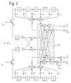
- HMM-Cells (same as filter bank) are described as shown in the block diagram of Fig. 1 and in greater detail in Fig. 2.
- the purpose of a single HMM-Cell is to demultiplex a complex-valued FDM-Signal into two subbands with the effect that the number of subband doubles and their respective sampling rate and the bandwidth carried by a signal is decimated by two.
- the gate count in the ASIC can be significantly reduced for the signal processing elements if only a single HMM-Cell is deployed in each stage of the tree.
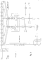
- This concept leads to a time-multiplex HMM structure. Multiplexed data processing is being carried out for real and imaginary parts of the signal and for the signals associated with the different subbands. Multiplexing is confined to one stage in the tree structure. According to this concept 4 HMM-Cells are implemented in the ASIC.
- the register elements are replaced by delay lines (which implement a shift register) and matched to the number of subbands to be processed.
- Fig. 2 illustrates the basic functions carried out in a HMM-Cell.
- Each HMM-structure consists of two decimation filters that decompose the input signal into the two subbands.
- decimation filters are implemented as a low-pass and a band-pass filter that is followed by a down converter.
- the signal flow diagram in Fig. 2 shows that both filters consist of identical FIR filter structures with coefficients only differing in sign. This property is the key to the sequential implementation of the filter bank.
- the adder of the basic FIR filter structure outputs the operands for subsequent summations.
- the operands must be intermediately stored for sequential processing, as shown in Fig. 3.
- Multiplication with -1, depicted as minus sign at the adder inputs, are carried out through data inversion and setting the carry bit at the LSB position of the following adder to 1.
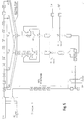
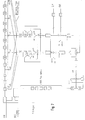
- Fig. 5 through Fig. 8 illustrate the switch positions for the four computation cycles.
- the HMM-Cell needs two new input samples to enable computation of a new output sample.
- This behaviour can also be seen in Fig. 2 where an input switch distributes data of one type to registers that operate at half of the sampling frequency.
- Fig. 3 the same behaviour is obtained by using two registers instead of one that both run on the input sampling rate, but are being fed by real and imaginary data part in sequence.
- the computations of the filter must take place each time a data sample is fed into the filter structure.
- HMM-Cells placed at lower hierarchy than the first are fed with a time-multiplexed signal at the input. Those cells still require the presence of two complex-valued samples of the same subband in its delay lines before computations can commence.
- This new situation is obviated by a modified input switch circuit at the filter input, illustrated in Fig. 9, 10, and 11.
- This input switch uses the fact that it is irrelevant which delay line is fed with the first or the second data sample.
- the input switch circuit consists of three registers and two pairs of switches. The input switches alternate with every clock cycle while the output switches in the second HMM stage alternate only every second cycle, in the third HMM stage only every fourth cycle and so on. This has the effect that the spacing between samples of the same subband type can be compensated in a single delay line which is the one that feeds the coefficient c0.
- the arithmetic section of the filter determines the maximum speed of the design. Multiplication are carried out using CSD-Code coefficient representation along with a Wallace-Tree structure. Each HMM-Cell consists of two separate Wallace-Trees as shown in Fig. 3.
- FIFO first-in first-out
Landscapes
- Engineering & Computer Science (AREA)
- Physics & Mathematics (AREA)
- Computer Hardware Design (AREA)
- Mathematical Physics (AREA)
- Signal Processing (AREA)
- Computer Networks & Wireless Communication (AREA)
- Radio Relay Systems (AREA)
- Time-Division Multiplex Systems (AREA)
- Data Exchanges In Wide-Area Networks (AREA)
- Compression Or Coding Systems Of Tv Signals (AREA)
Claims (2)
- Verfahren zum digitalen FDM-Demultiplexieren durch einen hierarchisch aufgebauten, mehrstufigen digitalen FDM-Demultiplexer, in dem viele verschiedene digitale Filterbänke benutzt werden, bestehend aus HMM-Zellen, die hintereinander angeordnet sind zum Auszweigen in aufeinanderfolgenden Stufen zu einer Baumstruktur entsprechend der "Hierarchical Multistage Method (HMM)", wobei beginnend bei der ersten Stufe jede HMM-Zelle ein jeweiliges komplexwertiges FDM-Signal in zwei Subbänder mit jedesmal reduzierter Abtastfrequenz demultiplexiert, dadurch gekennzeichnet, daß:in jeder HMM-Zelle selbst Verarbeitung multiplexierter Daten erfolgt für reale und imaginäre Signalteile und für Daten von verschiedenen Subbändern;am Eingang jeder HMM-Zelle eine Schaltschaltung abwechselnd die ungerade und gerade Zapf-Verzögerungsstrecke der HMM-Zelle mit Daten speist, die von jeweils aufeinanderfolgenden Zeitpunkten stammen;von jeder Hierarchieebene zur nächsten in einer HMM-Zelle die Zahl der Verzögerungselemente zwischen zwei Koeffizienten-Zapfstellen sich verdoppelt;jede der zweiten und folgenden HMM-Zellen mit einem viele Subbänder tragenden Multiplexsignal gespeist wird.
- Verfahren nach Anspruch 1, dadurch gekennzeichnet, daß alle Verzögerungsstrecken der HMM-Zellen mit mehr als zwei Verzögerungselementen unter Verwendung eines FIFO-Speichers implementiert werden.
(Beschriftung der Figuren:)
Stage = Stufe
Realization = Realisierung
Priority Applications (4)
| Application Number | Priority Date | Filing Date | Title |
|---|---|---|---|
| AT92117468T ATE178446T1 (de) | 1992-10-13 | 1992-10-13 | Hierarchisch aufgebauter mehrstufiger digitaler fdm-demultiplexer |
| EP92117468A EP0616452B1 (de) | 1992-10-13 | 1992-10-13 | Hierarchisch aufgebauter mehrstufiger digitaler FDM-Demultiplexer |
| DE69228826T DE69228826T2 (de) | 1992-10-13 | 1992-10-13 | Hierarchisch aufgebauter mehrstufiger digitaler FDM-Demultiplexer |
| ES92117468T ES2133297T3 (es) | 1992-10-13 | 1992-10-13 | Demultiplexor fdm digital polietapico jerarquico. |
Applications Claiming Priority (1)
| Application Number | Priority Date | Filing Date | Title |
|---|---|---|---|
| EP92117468A EP0616452B1 (de) | 1992-10-13 | 1992-10-13 | Hierarchisch aufgebauter mehrstufiger digitaler FDM-Demultiplexer |
Publications (2)
| Publication Number | Publication Date |
|---|---|
| EP0616452A1 EP0616452A1 (de) | 1994-09-21 |
| EP0616452B1 true EP0616452B1 (de) | 1999-03-31 |
Family
ID=8210124
Family Applications (1)
| Application Number | Title | Priority Date | Filing Date |
|---|---|---|---|
| EP92117468A Expired - Lifetime EP0616452B1 (de) | 1992-10-13 | 1992-10-13 | Hierarchisch aufgebauter mehrstufiger digitaler FDM-Demultiplexer |
Country Status (4)
| Country | Link |
|---|---|
| EP (1) | EP0616452B1 (de) |
| AT (1) | ATE178446T1 (de) |
| DE (1) | DE69228826T2 (de) |
| ES (1) | ES2133297T3 (de) |
Families Citing this family (1)
| Publication number | Priority date | Publication date | Assignee | Title |
|---|---|---|---|---|
| US6259728B1 (en) * | 1999-06-08 | 2001-07-10 | Lucent Technologies Inc. | Data communication system and method |
Family Cites Families (3)
| Publication number | Priority date | Publication date | Assignee | Title |
|---|---|---|---|---|
| DE3610195A1 (de) * | 1986-03-26 | 1987-10-01 | Ant Nachrichtentech | Digitale filterbank |
| JPS63292813A (ja) * | 1987-05-26 | 1988-11-30 | Toshiba Corp | 多入力ディジタルフィルタ |
| EP0308649B1 (de) * | 1987-09-24 | 1994-06-08 | ANT Nachrichtentechnik GmbH | Digitaler Filterbaum |
-
1992
- 1992-10-13 AT AT92117468T patent/ATE178446T1/de not_active IP Right Cessation
- 1992-10-13 EP EP92117468A patent/EP0616452B1/de not_active Expired - Lifetime
- 1992-10-13 DE DE69228826T patent/DE69228826T2/de not_active Expired - Fee Related
- 1992-10-13 ES ES92117468T patent/ES2133297T3/es not_active Expired - Lifetime
Also Published As
| Publication number | Publication date |
|---|---|
| ES2133297T3 (es) | 1999-09-16 |
| EP0616452A1 (de) | 1994-09-21 |
| ATE178446T1 (de) | 1999-04-15 |
| DE69228826T2 (de) | 1999-08-26 |
| DE69228826D1 (de) | 1999-05-06 |
Similar Documents
| Publication | Publication Date | Title |
|---|---|---|
| US4393456A (en) | Digital filter bank | |
| US4777612A (en) | Digital signal processing apparatus having a digital filter | |
| US4199660A (en) | FDM/TDM Transmultiplexer | |
| US4117541A (en) | Configurable parallel arithmetic structure for recursive digital filtering | |
| US3665171A (en) | Nonrecursive digital filter apparatus employing delayedadd configuration | |
| CA1063184A (en) | Non-recursive digital filter employing simple coefficients | |
| US5757794A (en) | Digital down converter and method | |
| US4138730A (en) | High speed FFT processor | |
| US4896320A (en) | Filter bank for frequency demultiplexing in multiple channels | |
| US4270026A (en) | Interpolator apparatus for increasing the word rate of a digital signal of the type employed in digital telephone systems | |
| US4792943A (en) | Digital filter bank | |
| EP0476215B1 (de) | Mehrkanaliger Taktfrequenzreduzierer | |
| US5258939A (en) | Fold and decimate filter architecture | |
| US4766561A (en) | Method and apparatus for implementing multiple filters with shared components | |
| US5548542A (en) | Half-band filter and method | |
| US5587939A (en) | Half-band filter for a cellular group demultiplexer | |
| US5270953A (en) | Fast convolution multiplier | |
| US4791597A (en) | Multiplierless FIR digital filter with two to the Nth power coefficients | |
| US5699363A (en) | Digital signal processing apparatus | |
| US5247515A (en) | Apparatus for extracting one from many multiplexed signals | |
| WO2001065692A1 (en) | Apparatus for splitting the frequency band of an input signal | |
| EP0180989B1 (de) | Digitaler Filter zur Änderung der Abtastfrequenz | |
| US7290021B2 (en) | Method and apparatus for parallel signal processing | |
| AU724637B2 (en) | Decimation method and decimation filter | |
| US4893264A (en) | Digital decimation filter |
Legal Events
| Date | Code | Title | Description |
|---|---|---|---|
| PUAI | Public reference made under article 153(3) epc to a published international application that has entered the european phase |
Free format text: ORIGINAL CODE: 0009012 |
|
| AK | Designated contracting states |
Kind code of ref document: A1 Designated state(s): AT CH DE ES FR GB IT LI NL |
|
| 17P | Request for examination filed |
Effective date: 19941031 |
|
| RAP1 | Party data changed (applicant data changed or rights of an application transferred) |
Owner name: ROBERT BOSCH GMBH |
|
| 17Q | First examination report despatched |
Effective date: 19970715 |
|
| GRAG | Despatch of communication of intention to grant |
Free format text: ORIGINAL CODE: EPIDOS AGRA |
|
| GRAG | Despatch of communication of intention to grant |
Free format text: ORIGINAL CODE: EPIDOS AGRA |
|
| GRAH | Despatch of communication of intention to grant a patent |
Free format text: ORIGINAL CODE: EPIDOS IGRA |
|
| GRAH | Despatch of communication of intention to grant a patent |
Free format text: ORIGINAL CODE: EPIDOS IGRA |
|
| GRAA | (expected) grant |
Free format text: ORIGINAL CODE: 0009210 |
|
| AK | Designated contracting states |
Kind code of ref document: B1 Designated state(s): AT CH DE ES FR GB IT LI NL |
|
| REF | Corresponds to: |
Ref document number: 178446 Country of ref document: AT Date of ref document: 19990415 Kind code of ref document: T |
|
| REG | Reference to a national code |
Ref country code: CH Ref legal event code: NV Representative=s name: SCINTILLA AG, DIREKTION Ref country code: CH Ref legal event code: EP |
|
| REF | Corresponds to: |
Ref document number: 69228826 Country of ref document: DE Date of ref document: 19990506 |
|
| ET | Fr: translation filed | ||
| REG | Reference to a national code |
Ref country code: ES Ref legal event code: FG2A Ref document number: 2133297 Country of ref document: ES Kind code of ref document: T3 |
|
| PG25 | Lapsed in a contracting state [announced via postgrant information from national office to epo] |
Ref country code: AT Free format text: LAPSE BECAUSE OF NON-PAYMENT OF DUE FEES Effective date: 19991013 |
|
| PG25 | Lapsed in a contracting state [announced via postgrant information from national office to epo] |
Ref country code: ES Free format text: LAPSE BECAUSE OF NON-PAYMENT OF DUE FEES Effective date: 19991014 |
|
| PG25 | Lapsed in a contracting state [announced via postgrant information from national office to epo] |
Ref country code: LI Free format text: LAPSE BECAUSE OF NON-PAYMENT OF DUE FEES Effective date: 19991031 Ref country code: CH Free format text: LAPSE BECAUSE OF NON-PAYMENT OF DUE FEES Effective date: 19991031 |
|
| PLBE | No opposition filed within time limit |
Free format text: ORIGINAL CODE: 0009261 |
|
| STAA | Information on the status of an ep patent application or granted ep patent |
Free format text: STATUS: NO OPPOSITION FILED WITHIN TIME LIMIT |
|
| 26N | No opposition filed | ||
| PG25 | Lapsed in a contracting state [announced via postgrant information from national office to epo] |
Ref country code: NL Free format text: LAPSE BECAUSE OF NON-PAYMENT OF DUE FEES Effective date: 20000501 |
|
| REG | Reference to a national code |
Ref country code: CH Ref legal event code: PL |
|
| NLV4 | Nl: lapsed or anulled due to non-payment of the annual fee |
Effective date: 20000501 |
|
| PGFP | Annual fee paid to national office [announced via postgrant information from national office to epo] |
Ref country code: GB Payment date: 20010926 Year of fee payment: 10 |
|
| PGFP | Annual fee paid to national office [announced via postgrant information from national office to epo] |
Ref country code: FR Payment date: 20011017 Year of fee payment: 10 |
|
| PGFP | Annual fee paid to national office [announced via postgrant information from national office to epo] |
Ref country code: DE Payment date: 20011211 Year of fee payment: 10 |
|
| REG | Reference to a national code |
Ref country code: GB Ref legal event code: IF02 |
|
| PG25 | Lapsed in a contracting state [announced via postgrant information from national office to epo] |
Ref country code: GB Free format text: LAPSE BECAUSE OF NON-PAYMENT OF DUE FEES Effective date: 20021013 |
|
| PG25 | Lapsed in a contracting state [announced via postgrant information from national office to epo] |
Ref country code: DE Free format text: LAPSE BECAUSE OF NON-PAYMENT OF DUE FEES Effective date: 20030501 |
|
| GBPC | Gb: european patent ceased through non-payment of renewal fee |
Effective date: 20021013 |
|
| PG25 | Lapsed in a contracting state [announced via postgrant information from national office to epo] |
Ref country code: FR Free format text: LAPSE BECAUSE OF NON-PAYMENT OF DUE FEES Effective date: 20030630 |
|
| REG | Reference to a national code |
Ref country code: FR Ref legal event code: ST |
|
| REG | Reference to a national code |
Ref country code: ES Ref legal event code: FD2A Effective date: 20001113 |
|
| PG25 | Lapsed in a contracting state [announced via postgrant information from national office to epo] |
Ref country code: IT Free format text: LAPSE BECAUSE OF NON-PAYMENT OF DUE FEES;WARNING: LAPSES OF ITALIAN PATENTS WITH EFFECTIVE DATE BEFORE 2007 MAY HAVE OCCURRED AT ANY TIME BEFORE 2007. THE CORRECT EFFECTIVE DATE MAY BE DIFFERENT FROM THE ONE RECORDED. Effective date: 20051013 |