EP0617382B1 - Carte de crédit avec une pièce enfichable amovible - Google Patents
Carte de crédit avec une pièce enfichable amovible Download PDFInfo
- Publication number
- EP0617382B1 EP0617382B1 EP94104785A EP94104785A EP0617382B1 EP 0617382 B1 EP0617382 B1 EP 0617382B1 EP 94104785 A EP94104785 A EP 94104785A EP 94104785 A EP94104785 A EP 94104785A EP 0617382 B1 EP0617382 B1 EP 0617382B1
- Authority
- EP
- European Patent Office
- Prior art keywords
- recess
- card
- authorisation
- authorisation card
- push
- Prior art date
- Legal status (The legal status is an assumption and is not a legal conclusion. Google has not performed a legal analysis and makes no representation as to the accuracy of the status listed.)
- Expired - Lifetime
Links
Images

Classifications
-
- G—PHYSICS
- G06—COMPUTING OR CALCULATING; COUNTING
- G06K—GRAPHICAL DATA READING; PRESENTATION OF DATA; RECORD CARRIERS; HANDLING RECORD CARRIERS
- G06K19/00—Record carriers for use with machines and with at least a part designed to carry digital markings
- G06K19/06—Record carriers for use with machines and with at least a part designed to carry digital markings characterised by the kind of the digital marking, e.g. shape, nature, code
- G06K19/067—Record carriers with conductive marks, printed circuits or semiconductor circuit elements, e.g. credit or identity cards also with resonating or responding marks without active components
- G06K19/07—Record carriers with conductive marks, printed circuits or semiconductor circuit elements, e.g. credit or identity cards also with resonating or responding marks without active components with integrated circuit chips
- G06K19/077—Constructional details, e.g. mounting of circuits in the carrier
- G06K19/07737—Constructional details, e.g. mounting of circuits in the carrier the record carrier consisting of two or more mechanically separable parts
- G06K19/07739—Constructional details, e.g. mounting of circuits in the carrier the record carrier consisting of two or more mechanically separable parts comprising a first part capable of functioning as a record carrier on its own and a second part being only functional as a form factor changing part, e.g. SIM cards type ID 0001, removably attached to a regular smart card form factor
-
- G—PHYSICS
- G06—COMPUTING OR CALCULATING; COUNTING
- G06K—GRAPHICAL DATA READING; PRESENTATION OF DATA; RECORD CARRIERS; HANDLING RECORD CARRIERS
- G06K19/00—Record carriers for use with machines and with at least a part designed to carry digital markings
- G06K19/04—Record carriers for use with machines and with at least a part designed to carry digital markings characterised by the shape
-
- G—PHYSICS
- G06—COMPUTING OR CALCULATING; COUNTING
- G06K—GRAPHICAL DATA READING; PRESENTATION OF DATA; RECORD CARRIERS; HANDLING RECORD CARRIERS
- G06K19/00—Record carriers for use with machines and with at least a part designed to carry digital markings
- G06K19/06—Record carriers for use with machines and with at least a part designed to carry digital markings characterised by the kind of the digital marking, e.g. shape, nature, code
- G06K19/067—Record carriers with conductive marks, printed circuits or semiconductor circuit elements, e.g. credit or identity cards also with resonating or responding marks without active components
- G06K19/07—Record carriers with conductive marks, printed circuits or semiconductor circuit elements, e.g. credit or identity cards also with resonating or responding marks without active components with integrated circuit chips
- G06K19/077—Constructional details, e.g. mounting of circuits in the carrier
Definitions
- the invention relates to a prepaid card with international Standardization of the external dimensions and the position of the Contact surface of an implanted semiconductor chip, the Semiconductor chip on one in its dimensions compared to the Prepaid card is arranged much smaller plug-in part, which insert part arranged in a in the prepaid card Recess in the press fit and is held interchangeably, the recess in the prepaid card being arranged in such a way that the prepaid card with the inserted part remains usable for other prepaid card applications and if necessary, the insert itself as an independent Mini chip card can be used in much smaller devices is.
- a prepaid card with the aforementioned features is in the DE 38 04 361 C1 described.
- Credit or debit card for ATMs, Card phones, other communication devices or also identification cards for access control of value cards serving security-sensitive areas are subject to one in terms of their dimensions international standardization; this also applies to the meantime known under the term SIM module cards and in their dimensions are only about a tenth of their size cards for the operation of customary prepaid cards of handheld phones as small end devices.
- DE 38 04 361 C1 describes an appropriate combination the prepaid cards with the SIM module cards by the SIM module cards as insert parts in the prepaid cards can be integrated.
- the prepaid card points to the corresponding place on a recess in which the Insert part is held in the press fit.
- This recess is arranged as an open recess in the known solution, whereby to bring about the clamping fit of the plug-in part in the recess, the circumferential associated with each other side edges of insert and recess coordinated designs in the form of bulges / fillets exhibit.
- hiring a manageable Clamping seat on the dimensions of the shapes of the Side edges of insert and recess is difficult; either the clamping effect is too low or the snap-in resistance is too large, with the risk that the plug-in part when clipping into the prepaid card great effort through the prepaid card becomes.
- the dimensions of the SIM module card a tolerance deviation as the standard defining the insert of 0.1 mm each, which raises the problem of correct dimensioning of the clamping effect is reinforced.
- the invention is therefore based on the object generic value card the holder of the plug in to improve the prepaid card.
- the basic idea of the invention provides that for Tolerance compensation at least one boundary edge of the Recess to accommodate the insert part in the prepaid card is provided with a resilient clamp design, the thus predetermined dimensions of the recess on the smallest size of a SIM module card as Plug-in cards are parked while permissible Deviations from those at the boundary edges of the Resilient clamp design provided in the recess is to be balanced. This is an advantage Improvement of the clamping fit of the insert part in the Given prepaid card.
- each one of two opposing boundary edges has a resilient clamp design to a secure fit of the insert in the recess of the Prepaid card also taking into account the to ensure permissible manufacturing tolerances.
- Farther can of course all boundary edges of the recess have a resilient clamp design.
- Realization of tolerance compensation suggested that the boundary edges of the recess in a wavy shape Course with a sequence of increases and decreases are trained and that each increase one in a vertical Distance to form a resilient web arranged hole assigned in the prepaid card is. It has been found that the usual used to make corresponding cards Plastics a width of the web in the order of magnitude between 2 and 5 tenths of a millimeter is sufficient to achieve the ensure the desired spring action. Other clamp designs too such as at the boundary edges molded webs are included in the invention.
- the prepaid card Recess in the prepaid card on one side by means of a cover closed; this will be more advantageous Make a storage space closed to one side created for the insert part, so that in more advantageous Way the danger is avoided that the male part due to the comparatively thin prepaid card can be pushed through. Furthermore, with this Execution of the advantage associated that after inserting the Insert part in the one-sided through the Covered recess area of the prepaid card Push-in part by pressing on the cover again easily removed from the recess of the prepaid card can be. To form the cover, the Making the recess by milling also a thin one The base plate remains as a cover for the recess. Alternatively, apply a thin, tear-resistant film provided on the corresponding side of the prepaid card.
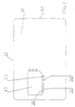
- the value card shown in Figure 1 corresponds in length and width of the ISO standard, and the rectangular Value card 10 has 11 on its longer side edges a dimension of 85.5 mm and 12 on its shorter side edges a dimension of 54.0 mm, with a material thickness of 0.86 mm with the permissible deviation of ⁇ 0.1 mm.
- the outer corners of the prepaid card 10 are with a Rounded radius of 2.0 mm.
- a recess 13 is arranged, the dimensions of which Dimensions of a plug-in part shown in Figure 2 14 are coordinated so that the insertion part 14 in the Recess 13 of the prepaid card 10 by means of a press fit is captured.
- the insertion part 14 is in particular as SIM module card according to the applicable standard educated.
- the recess 13 is on the Value card 10 at a point where a standard Phone card, for example, also the chips with the assigned stored value information arranged are.
- the plug-in part 14 addressed in FIG. 2 is in its Dimensions much smaller, and he points in this example given a chamfered corner. This results in a dimension of for the longer longitudinal edge 15 25.1 mm, for the shorter longitudinal edge 16 one of 22.6 mm, while the longer transverse edge 17 a total of 15.1 mm measures and the shorter transverse edge 18 a dimension of 12.6 mm having; the chamfer 19 is 2.5 mm long.
- the back is the Value card 10 provided with a thin cover 20, so that the receiving space resulting from FIG. 1 for the insertion part 14 is completed on the back;
- the Cover 20 is, for example, in a manner known per se to be provided with advertising imprints or other information.
- the cover 20 can either be as shown in Figure 4 formed by a thin but tear-resistant film be, or it can be from milling the recess 13 card 10 is left a thin bottom surface.
- FIGS. 1 or 3 shown recording card 10 are clipped; the The insertion part 14 is removed by external pressure on the cover 20 of the prepaid card 10, so that the Insert part held in the recess 13 in the press fit 14 emerges from the recess 13.
Landscapes
- Engineering & Computer Science (AREA)
- Physics & Mathematics (AREA)
- General Physics & Mathematics (AREA)
- Theoretical Computer Science (AREA)
- Computer Hardware Design (AREA)
- Microelectronics & Electronic Packaging (AREA)
- Coupling Device And Connection With Printed Circuit (AREA)
- Telephone Set Structure (AREA)
- Details Of Connecting Devices For Male And Female Coupling (AREA)
- Credit Cards Or The Like (AREA)
Claims (10)
- Carte à mémoire (10) dont les dimensions et l'emplacement de la surface de contact d'une puce à semi-conducteur insérée satisfont à la normalisation internationale, la puce à semi-conducteur étant disposée sur un élément enfichable (14) dont les dimensions sont nettement inférieures à celles de la carte à mémoire, lequel élément enfichable (14) étant ajusté, de manière amovible et par pression dans un évidement (13) agencé dans la carte à mémoire (10), l'évidement (13) étant agencé de telle sorte dans la carte à mémoire (10) que la carte à mémoire (10), lorsque l'élément enfichable (14) y est intégré, puisse également être utilisée dans le cadre d'autres applications de carte à mémoire et que l'élément enfichable (14) puisse, le cas échéant, être lui-même utilisé comme une mini carte à puce indépendante dans des terminaux de taille sensiblement inférieure, caractérisée en ce que, en vue de respecter les tolérances, au moins une arête délimitant l'évidement (13) prévu dans la carte à mémoire (10) pour loger l'élément enfichable (14) est dotée d'une structure de fixation élastique (33).
- Carte à mémoire selon la revendication 1, caractérisée en ce que deux arêtes délimitant l'évidement (13) sont dotées d'une structure de fixation élastique (33).
- Carte à mémoire selon la revendication 2, caractérisée en ce que toutes les arêtes délimitant l'évidement (13) présentent une structure de fixation élastique (33).
- Carte à mémoire selon la revendication 2, caractérisée en ce que respectivement l'une des deux arêtes de délimitation opposées l'une par rapport à l'autre présente une structure de fixation élastique (33).
- Carte à mémoire selon l'une des revendications 1 à 4, caractérisée en ce que les arêtes délimitant l'évidement (13) sont réalisées en forme d'onde et présentent une succession de bosses (30) et de creux (31), et en ce que chaque bosse (30) correspond dans la carte à mémoire (10)un alésage (32), situé à une certaine distance de celle-ci sur la verticale pour former une tige élastique (33).
- Carte à mémoire selon la revendication 5, caractérisée en ce que la largeur des tiges (33) est de 0,2 à 0,5 mm.
- Carte à mémoire selon l'une des revendications 1 à 6, caractérisée en ce que l'évidement (13) de la carte à mémoire (10) est obturé sur un de ses côtés à l'aide d'un cache (20).
- Carte à mémoire selon la revendication 7, caractérisée en ce que le cache (20) est constitué d'une feuille recouvrant la carte à mémoire du côté concerné.
- Carte à mémoire selon la revendication 7, caractérisée en ce que l'évidement (13) de la carte à mémoire (10) est fraisé pour laisser une surface faisant office de cache (20) pour l'évidement (13).
- Carte à mémoire selon l'une des revendications 1 à 9, caractérisée en ce que, afin de loger deux éléments enfichables (14), la carte à mémoire (10) présente deux évidements (13) orientés en fonction des arêtes à insérer (12) opposées l'une à l'autre.
Applications Claiming Priority (8)
| Application Number | Priority Date | Filing Date | Title |
|---|---|---|---|
| DE9304499U | 1993-03-26 | ||
| DE9304499U DE9304499U1 (de) | 1993-03-26 | 1993-03-26 | Aufbewahrungskarte für eine SIM-Modul-Karte |
| DE9309996U | 1993-07-06 | ||
| DE9309997 | 1993-07-06 | ||
| DE9309996 | 1993-07-06 | ||
| DE9309997U | 1993-07-06 | ||
| DE9312755U | 1993-08-27 | ||
| DE9312755U DE9312755U1 (de) | 1993-08-27 | 1993-08-27 | Aufbewahrungskarte für eine SIM-Modulkarte |
Publications (3)
| Publication Number | Publication Date |
|---|---|
| EP0617382A2 EP0617382A2 (fr) | 1994-09-28 |
| EP0617382A3 EP0617382A3 (fr) | 1995-04-26 |
| EP0617382B1 true EP0617382B1 (fr) | 1999-03-03 |
Family
ID=27436470
Family Applications (1)
| Application Number | Title | Priority Date | Filing Date |
|---|---|---|---|
| EP94104785A Expired - Lifetime EP0617382B1 (fr) | 1993-03-26 | 1994-03-25 | Carte de crédit avec une pièce enfichable amovible |
Country Status (4)
| Country | Link |
|---|---|
| EP (1) | EP0617382B1 (fr) |
| AT (1) | ATE177227T1 (fr) |
| DE (1) | DE59407855D1 (fr) |
| ES (1) | ES2131603T3 (fr) |
Families Citing this family (9)
| Publication number | Priority date | Publication date | Assignee | Title |
|---|---|---|---|---|
| US5514862A (en) * | 1994-05-20 | 1996-05-07 | At&T Corp. | Portable data carrier |
| ES2102317B1 (es) * | 1994-09-19 | 1998-04-16 | Nacional Moneda Timbre | Tarjeta inteligente de uso en telefonia y similar. |
| FR2734071B1 (fr) * | 1995-05-11 | 1997-06-06 | Schlumberger Ind Sa | Carte de paiement electronique a module interchangeable |
| DE29509736U1 (de) * | 1995-06-14 | 1996-04-04 | Giesecke & Devrient GmbH, 81677 München | Standardkarte mit eingelagerter Minichipkarte |
| DE19650048A1 (de) * | 1996-12-03 | 1998-06-04 | Bayerische Motoren Werke Ag | Speicher für benutzerindividuelle Einstelldaten von Fahrzeug-Ausrüstungsteilen |
| FR2776889A1 (fr) * | 1998-03-26 | 1999-10-01 | Rene Teaupel | Platine amovible electronique |
| DE19817297C2 (de) * | 1998-04-18 | 2003-08-14 | Orga Kartensysteme Gmbh | Trägerkarte |
| DE10050960A1 (de) * | 2000-06-28 | 2002-01-17 | Tronic Mgm Ag Urdorf A | Transport- oder Beförderungseinheit für einen Chip, insbesondere einen Telefon-Chip |
| WO2004070664A1 (fr) * | 2003-02-06 | 2004-08-19 | Nagracard Sa | Procede de fabrication d'un module de securite destine notamment au controle d'acces et module de securite obtenu selon ce procede |
Family Cites Families (4)
| Publication number | Priority date | Publication date | Assignee | Title |
|---|---|---|---|---|
| FR2538930B1 (fr) * | 1983-01-05 | 1989-05-19 | Seiichiro Aigo | Carte d'information |
| JPS6143388A (ja) * | 1984-08-08 | 1986-03-01 | Mitsubishi Plastics Ind Ltd | メモリ−カ−ド |
| DE3804361C1 (fr) * | 1988-02-12 | 1988-09-29 | Deutsche Bundespost, Vertreten Durch Den Praesidenten Des Fernmeldetechnischen Zentralamtes, 6100 Darmstadt, De | |
| DE4040296C1 (fr) * | 1990-12-17 | 1992-01-09 | Orga Kartensysteme Gmbh, 6072 Dreieich, De |
-
1994
- 1994-03-25 ES ES94104785T patent/ES2131603T3/es not_active Expired - Lifetime
- 1994-03-25 AT AT94104785T patent/ATE177227T1/de not_active IP Right Cessation
- 1994-03-25 DE DE59407855T patent/DE59407855D1/de not_active Expired - Fee Related
- 1994-03-25 EP EP94104785A patent/EP0617382B1/fr not_active Expired - Lifetime
Also Published As
| Publication number | Publication date |
|---|---|
| EP0617382A3 (fr) | 1995-04-26 |
| ATE177227T1 (de) | 1999-03-15 |
| ES2131603T3 (es) | 1999-08-01 |
| DE59407855D1 (de) | 1999-04-08 |
| EP0617382A2 (fr) | 1994-09-28 |
Similar Documents
| Publication | Publication Date | Title |
|---|---|---|
| DE69213555T2 (de) | Kontaktgeber für Karten mit Schaltkreis | |
| DE69504259T2 (de) | Tragbare Schnittstelle für elektronische Chipkarte | |
| DE10321348B4 (de) | Steckverbinder | |
| DE69834302T2 (de) | Chipkarten-Verbinder | |
| DE60023650T2 (de) | Kartenverbinder | |
| DE4029576A1 (de) | Kontaktiereinrichtung fuer standard-chipkarte und sim-karte | |
| DE69721325T2 (de) | Kartenhalter | |
| EP0495216A2 (fr) | Carte d'identité avec un microprocesseur | |
| DE3937383A1 (de) | Aufnahmevorrichtung fuer chipkarten | |
| EP0866413A2 (fr) | Adaptateur pour le contact de porteurs au format carte | |
| DE19913923A1 (de) | Kontaktiereinrichtung für eine SIM-Karte | |
| EP0617382B1 (fr) | Carte de crédit avec une pièce enfichable amovible | |
| DE69937103T2 (de) | Tragbare Chipkarten-Leseanordnung | |
| DE19826428A1 (de) | Chipmodul mit Aufnahmekörper | |
| DE29819389U1 (de) | Chipkarte | |
| DE60007151T2 (de) | Biegesteifte karte mit trennbarem modul | |
| DE19925146A1 (de) | Steckkarte für elektronische Geräte | |
| DE69636234T2 (de) | Entfernbare karte mit einer steckverbindung als smartkartenleser für einen mikrocomputer | |
| DE10332583B4 (de) | Kartenverbinderanordnung | |
| DE3544034C2 (fr) | ||
| EP0833271A2 (fr) | Lecteur de cartes à puce | |
| DE19815549C2 (de) | Steckkarte für elektronische Geräte | |
| DE9316522U1 (de) | Hülle für mindestens eine Karte mit Magnetstreifen | |
| DE19729397A1 (de) | Anordnung zur Aufnahme kartenförmiger Datenträger | |
| DE69422868T2 (de) | Elektronischer Terminal mit Speicherkartenleser |
Legal Events
| Date | Code | Title | Description |
|---|---|---|---|
| PUAI | Public reference made under article 153(3) epc to a published international application that has entered the european phase |
Free format text: ORIGINAL CODE: 0009012 |
|
| AK | Designated contracting states |
Kind code of ref document: A2 Designated state(s): AT BE CH DE DK ES FR GB GR IE IT LI LU MC NL PT SE |
|
| PUAL | Search report despatched |
Free format text: ORIGINAL CODE: 0009013 |
|
| AK | Designated contracting states |
Kind code of ref document: A3 Designated state(s): AT BE CH DE DK ES FR GB GR IE IT LI LU MC NL PT SE |
|
| 17P | Request for examination filed |
Effective date: 19950927 |
|
| GRAG | Despatch of communication of intention to grant |
Free format text: ORIGINAL CODE: EPIDOS AGRA |
|
| GRAG | Despatch of communication of intention to grant |
Free format text: ORIGINAL CODE: EPIDOS AGRA |
|
| GRAH | Despatch of communication of intention to grant a patent |
Free format text: ORIGINAL CODE: EPIDOS IGRA |
|
| 17Q | First examination report despatched |
Effective date: 19980810 |
|
| GRAH | Despatch of communication of intention to grant a patent |
Free format text: ORIGINAL CODE: EPIDOS IGRA |
|
| GRAA | (expected) grant |
Free format text: ORIGINAL CODE: 0009210 |
|
| AK | Designated contracting states |
Kind code of ref document: B1 Designated state(s): AT BE CH DE DK ES FR GB GR IE IT LI LU MC NL PT SE |
|
| PG25 | Lapsed in a contracting state [announced via postgrant information from national office to epo] |
Ref country code: SE Free format text: THE PATENT HAS BEEN ANNULLED BY A DECISION OF A NATIONAL AUTHORITY Effective date: 19990303 Ref country code: GR Free format text: LAPSE BECAUSE OF NON-PAYMENT OF DUE FEES Effective date: 19990303 |
|
| REF | Corresponds to: |
Ref document number: 177227 Country of ref document: AT Date of ref document: 19990315 Kind code of ref document: T |
|
| REG | Reference to a national code |
Ref country code: CH Ref legal event code: EP |
|
| REG | Reference to a national code |
Ref country code: IE Ref legal event code: FG4D Free format text: GERMAN |
|
| PG25 | Lapsed in a contracting state [announced via postgrant information from national office to epo] |
Ref country code: LU Free format text: LAPSE BECAUSE OF NON-PAYMENT OF DUE FEES Effective date: 19990325 |
|
| REF | Corresponds to: |
Ref document number: 59407855 Country of ref document: DE Date of ref document: 19990408 |
|
| ITF | It: translation for a ep patent filed | ||
| PG25 | Lapsed in a contracting state [announced via postgrant information from national office to epo] |
Ref country code: DK Free format text: LAPSE BECAUSE OF FAILURE TO SUBMIT A TRANSLATION OF THE DESCRIPTION OR TO PAY THE FEE WITHIN THE PRESCRIBED TIME-LIMIT Effective date: 19990603 |
|
| PG25 | Lapsed in a contracting state [announced via postgrant information from national office to epo] |
Ref country code: PT Free format text: LAPSE BECAUSE OF FAILURE TO SUBMIT A TRANSLATION OF THE DESCRIPTION OR TO PAY THE FEE WITHIN THE PRESCRIBED TIME-LIMIT Effective date: 19990604 |
|
| GBT | Gb: translation of ep patent filed (gb section 77(6)(a)/1977) |
Effective date: 19990514 |
|
| ET | Fr: translation filed | ||
| REG | Reference to a national code |
Ref country code: CH Ref legal event code: NV Representative=s name: HANS RUDOLF GACHNANG PATENTANWALT |
|
| REG | Reference to a national code |
Ref country code: ES Ref legal event code: FG2A Ref document number: 2131603 Country of ref document: ES Kind code of ref document: T3 |
|
| PG25 | Lapsed in a contracting state [announced via postgrant information from national office to epo] |
Ref country code: MC Free format text: LAPSE BECAUSE OF NON-PAYMENT OF DUE FEES Effective date: 19990930 |
|
| REG | Reference to a national code |
Ref country code: IE Ref legal event code: FD4D |
|
| PLBE | No opposition filed within time limit |
Free format text: ORIGINAL CODE: 0009261 |
|
| STAA | Information on the status of an ep patent application or granted ep patent |
Free format text: STATUS: NO OPPOSITION FILED WITHIN TIME LIMIT |
|
| 26N | No opposition filed | ||
| PGFP | Annual fee paid to national office [announced via postgrant information from national office to epo] |
Ref country code: CH Payment date: 20010323 Year of fee payment: 8 Ref country code: BE Payment date: 20010323 Year of fee payment: 8 Ref country code: AT Payment date: 20010323 Year of fee payment: 8 |
|
| PGFP | Annual fee paid to national office [announced via postgrant information from national office to epo] |
Ref country code: NL Payment date: 20010326 Year of fee payment: 8 Ref country code: ES Payment date: 20010326 Year of fee payment: 8 |
|
| REG | Reference to a national code |
Ref country code: GB Ref legal event code: IF02 |
|
| PG25 | Lapsed in a contracting state [announced via postgrant information from national office to epo] |
Ref country code: AT Free format text: LAPSE BECAUSE OF NON-PAYMENT OF DUE FEES Effective date: 20020325 |
|
| PG25 | Lapsed in a contracting state [announced via postgrant information from national office to epo] |
Ref country code: ES Free format text: LAPSE BECAUSE OF NON-PAYMENT OF DUE FEES Effective date: 20020326 |
|
| PG25 | Lapsed in a contracting state [announced via postgrant information from national office to epo] |
Ref country code: LI Free format text: LAPSE BECAUSE OF NON-PAYMENT OF DUE FEES Effective date: 20020331 Ref country code: CH Free format text: LAPSE BECAUSE OF NON-PAYMENT OF DUE FEES Effective date: 20020331 Ref country code: BE Free format text: LAPSE BECAUSE OF NON-PAYMENT OF DUE FEES Effective date: 20020331 |
|
| BERE | Be: lapsed |
Owner name: *TEWES WILHELM Effective date: 20020331 |
|
| PG25 | Lapsed in a contracting state [announced via postgrant information from national office to epo] |
Ref country code: NL Free format text: LAPSE BECAUSE OF NON-PAYMENT OF DUE FEES Effective date: 20021001 |
|
| REG | Reference to a national code |
Ref country code: CH Ref legal event code: PL |
|
| NLV4 | Nl: lapsed or anulled due to non-payment of the annual fee |
Effective date: 20021001 |
|
| PGFP | Annual fee paid to national office [announced via postgrant information from national office to epo] |
Ref country code: DE Payment date: 20040305 Year of fee payment: 11 |
|
| PGFP | Annual fee paid to national office [announced via postgrant information from national office to epo] |
Ref country code: GB Payment date: 20040311 Year of fee payment: 11 |
|
| PGFP | Annual fee paid to national office [announced via postgrant information from national office to epo] |
Ref country code: FR Payment date: 20040318 Year of fee payment: 11 |
|
| REG | Reference to a national code |
Ref country code: ES Ref legal event code: FD2A Effective date: 20030410 |
|
| PG25 | Lapsed in a contracting state [announced via postgrant information from national office to epo] |
Ref country code: IT Free format text: LAPSE BECAUSE OF NON-PAYMENT OF DUE FEES;WARNING: LAPSES OF ITALIAN PATENTS WITH EFFECTIVE DATE BEFORE 2007 MAY HAVE OCCURRED AT ANY TIME BEFORE 2007. THE CORRECT EFFECTIVE DATE MAY BE DIFFERENT FROM THE ONE RECORDED. Effective date: 20050325 Ref country code: GB Free format text: LAPSE BECAUSE OF NON-PAYMENT OF DUE FEES Effective date: 20050325 |
|
| PG25 | Lapsed in a contracting state [announced via postgrant information from national office to epo] |
Ref country code: DE Free format text: LAPSE BECAUSE OF NON-PAYMENT OF DUE FEES Effective date: 20051001 |
|
| GBPC | Gb: european patent ceased through non-payment of renewal fee |
Effective date: 20050325 |
|
| PG25 | Lapsed in a contracting state [announced via postgrant information from national office to epo] |
Ref country code: FR Free format text: LAPSE BECAUSE OF NON-PAYMENT OF DUE FEES Effective date: 20051130 |
|
| REG | Reference to a national code |
Ref country code: FR Ref legal event code: ST Effective date: 20051130 |