EP0617440B1 - Dünnschichtkondensator und Verfahren zu seiner Herstellung - Google Patents
Dünnschichtkondensator und Verfahren zu seiner Herstellung Download PDFInfo
- Publication number
- EP0617440B1 EP0617440B1 EP94104369A EP94104369A EP0617440B1 EP 0617440 B1 EP0617440 B1 EP 0617440B1 EP 94104369 A EP94104369 A EP 94104369A EP 94104369 A EP94104369 A EP 94104369A EP 0617440 B1 EP0617440 B1 EP 0617440B1
- Authority
- EP
- European Patent Office
- Prior art keywords
- dielectric layer
- thin film
- metal
- substrate
- capacitor
- Prior art date
- Legal status (The legal status is an assumption and is not a legal conclusion. Google has not performed a legal analysis and makes no representation as to the accuracy of the status listed.)
- Expired - Lifetime
Links
Images


Classifications
-
- H—ELECTRICITY
- H01—ELECTRIC ELEMENTS
- H01G—CAPACITORS; CAPACITORS, RECTIFIERS, DETECTORS, SWITCHING DEVICES, LIGHT-SENSITIVE OR TEMPERATURE-SENSITIVE DEVICES OF THE ELECTROLYTIC TYPE
- H01G4/00—Fixed capacitors; Processes of their manufacture
- H01G4/30—Stacked capacitors
- H01G4/306—Stacked capacitors made by thin film techniques
Definitions
- the present invention relates to a laminated thin film capacitor and a method for producing the same.
- Barium titanate (BiTaO 3 ) having a perovskite crystal structure is widely used as a capacitor material since it is excellent in dielectric properties and has a high resistivity. Since barium titanate is characterized in that its dielectric constant in the a axis is larger than that in the c axis which is a polarization axis, it can provide a capacitor having good dielectric properties when its a axis is orientated preferentially in a direction perpendicular to a plane of an electrode, that is, in the (100) plane.
- Strontium titanate (SrTiO 3 ) having a perovskite crystal structure is a cubic system crystal and paradielectric at a temperature of about 110 K or higher. While a ceramic comprising SrTiO 3 has a lower dielectric constant than a ceramic comprising BaTiO 3 having the same crystal structure, the former has better temperature characteristics and smaller dielectric loss than the latter.
- a shifter such as barium to SrTiO 3
- a ceramic which is paradielectric and has a high dielectric constant at room temperature is obtained. This kind of ceramic is extensively used in a capacitor for high frequency and high voltage.
- Powder of a dielectric material such as BaTiO 3 is compounded, mixed and dried.
- a slurry of the dielectric material powder is prepared and formed in a thin film sheet.
- An internal electrode paste of an electrode material such as palladium is printed on the sheet. These steps are repeated for determined times to alternately laminate the internal electrodes and the sheets. Thereafter, the laminate is cut to a desired size, and heated, whereby the ceramic and the metal are simultaneously sintered.
- a thickness of the dielectric layer there is a limitation on a thickness of the dielectric layer. That is, since a particle size of the dielectric material powder which is a raw material of the dielectric layer is about 1 ⁇ m, some problems arise in evenness of the film thickness or insulation between the electrodes when the dielectric layer having a thickness of 3 ⁇ m or less is formed by preparing the slurry of the powder, making the sheet from the slurry and sintering the sheet. To produce a chip capacitor having the large capacity, the number of laminated layers should be increased. However, when the number of laminated layers is increased, a size of a chip is enlarged and the number of production steps increases, so that the reliability of the capacitor may be deteriorated. In addition, since the sintering step is necessary after the lamination in the above method and the sintering temperature is as high as about 1200°C, an electrode material is limited to a high melting point metal such as platinum.
- An object of the present invention is to provide a novel laminated thin film capacitor and a method for producing the same.
- Another object of the present invention is to decrease a size of a chip capacitor while increasing its capacity.
- a further object of the present invention is to provide a method for easily forming a dielectric thin layer of a laminated thin film capacitor at a low temperature.
- the present invention first forms a pattern of a metal electrode layer on a substrate by vacuum deposition or sputtering.
- a film of a perovskite oxide such as BaTiO 3 , SrTiO 3 or (Ba 1-x Sr x )TiO 3 or a film of a composite perovskite compound of Pb[(Mg 1/3 Nb 2/3 ) 1-x Ti x ] which is preferentially orientated in the (100) plane is formed in a thickness of 0.05 to 3 ⁇ m by a plasma CVD method which utilizes activity of plasma and the CVD reaction.
- the above steps are repeated to laminate the metal electrode layers and the dielectric layers alternately.
- the laminate is cut to a predetermined size, and external electrodes are formed on both cut surfaces by vacuum deposition, sputtering, plating, coating-baking to obtain the laminated thin film capacitor.
- the dense thin film of (Ba 1-x Sr x )TiO 3 being preferentially orientated in the a axis direction or Pb[(Mg 1/3 Nb 2/3 ) 1-x Ti x ]O 3 both of which have good dielectric properties can be formed on the metal electrode layer at a lower temperature than the sintering temperature of a bulk or the temperature in other film formation methods such as vacuum deposition, sputtering and thermal CVD.
- the metal electrode layer is formed by vacuum deposition or sputtering, the dense metal electrode layer having a thickness of 0.01 to 0.2 ⁇ m can be formed.
- each layer has a thickness smaller than that formed from the slurry in the conventional laminated ceramic capacitor, a capacity of each dielectric layer can be made larger.
- the number of laminated layers in the same chip thickness can be increased. Consequently, an electrostatic capacity per unit volume is made large, so that the laminated thin film capacitor accommodating to the down-sizing and the capacity increase.
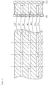
- Fig. 1 shows an apparatus for producing a laminated thin film capacitor, which comprises a plasma CVD unit for forming the dielectric layers and a sputtering unit for forming the metal electrode layers.
- the apparatus of Fig. 1 comprises a substrate-fixing plate 2 on which a base substrate 1 is held, a pre-evacuating room 3, a pre-heating room 4, a transfer arm 5, a substrate holder 6, a lamp heater 7, a gate 8, a sputtering chamber 9, a substrate holder 10, metal masks 11 and 12, a lamp heater 13, a mass flow controller 14, a target 15, a high frequency power source 16 (13.56 MHz), a motor 17 for rotating the substrate holder 6, a gate 18, a plasma CVD chamber 19, a substrate holder 20, a transfer arm 21, a motor for rotating the substrate holder 20, evaporation vessels 24, 26, 28 and 30, raw materials 25, 27, 29 and 31, mass flow controllers 32, 33, 34, 35 and 36, a nozzle 37 for supplying raw material gases and reaction gas, a high frequency power source 38 (13.56 MHz), an electrode 39, a motor 40 for rotating the substrate holder 10, and a pre-evacuating room 41.
- the laminated thin film capacitor of the present invention comprises a base substrate 42, metal electrode layers 43, 45 and 47, dielectric layers 44, 46 and 48, and external electrodes 49 and 50.
- the laminated thin film capacitor comprises a base substrate 51, metal electrode layers 52 and 54, and a dielectric layer 53.
- the substrate-fixing plate 2 on which the base substrate 1 made of alumina (sizes: 50 mm x 50 mm x 0.3 mm) is held, is transferred in the evacuated pre-heating room 4 via the pre-evacuating room 3.
- the substrate-fixing plate 2 is transferred onto the substrate holder 6 by the transfer arm 5, and the substrate holder 6 is heated to 650°C by the lamp heater 7.
- the gate 8 is opened, and the substrate-fixing plate 2 is transferred by the transfer arm 5 onto the substrate holder 10 in the sputtering chamber 9.
- two metal masks 11 and 12 are attached, and the two patterns of the metal electrode films as shown in Fig. 2 are alternately formed using the two masks alternately.
- Each metal mask has a size of 6.0 mm x 1.2 mm.
- the substrate-fixing plate is placed on the metal mask 11, and the base substrate 1 is intimately contacted to the metal mask 11.
- the substrate holder 10 is beforehand heated to 650°C by the lamp heater 13.
- the gate 8 is closed, and the sputtering chamber 9 is evacuated to 1 x 10 -4 Pa.
- argon gas is supplied in the sputtering chamber 9 with controlling a flow rate by the mass flow controller 14.
- plasma power of 0.8 W/cm 2
- the high frequency power source 16 13.56 MHz
- the metal electrode layer 43 having the thickness of about 0.05 ⁇ m is formed by 5 minutes sputtering.
- supply of the argon gas is stopped, the gate 8 is opened, and the substrate-fixing plate 2 is transferred on the substrate holder 6 by the transfer arm 5.
- the substrate holder 6 is half turned by the motor 17 so that the substrate-fixing plate 2 is transferred on the side of gate 18.
- the gate 18 is opened, and the substrate-fixing plate 2 is transferred on the substrate holder 20 in the plasma CVD chamber 19 by the transfer arm 21.
- the substrate holder 20 is beforehand heated to 650°C by the lamp heater 22.
- the gate 18 is closed, the plasma CVD chamber 19 is evacuated to 1 Pa, and the substrate holder 20 is rotated at 120 rpm by the motor 23.
- the raw material 25 barium dipivaloylmethane: Ba(C 11 H 19 O 2 ) 2
- the raw material 27 isopropoxy-titanium: Ti(C 3 H 7 O) 4
- the raw material 29 is beforehand charged, respectively and heated to and maintained at 230°C, 50°C and 240°C, respectively.
- Vapors of Ba(C 11 H 19 O 2 ) 2 , Ti(C 3 H 7 O) 4 and Sr(C 11 H 19 O 2 ) 2 are supplied into the plasma CVD chamber by flowing the argon carrier gas in the evaporation vessels 24, 26 and 28 respectively by adjusting the flow rates of the carrier gas at 50 cm 3 /min., 30 cm 3 /min. and 40 cm 3 /min. respectively by the mass flow controllers 32, 33 and 34, respectively.
- the reaction gas oxygen gas
- the raw material gasses and the reaction gas are supplied over the base substrate 2 through the nozzle 37.
- the plasma (power of 1.4 W/cm 2 ) is generated by the high frequency power source 38 (13.56 MHz) between the electrode 39 and the substrate holder 20 to form the dielectric layer 44 over the whole surface of the base substrate 1 carrying the metal electrode layer 43. Since a film forming rate of the (Ba 1-x Sr x )TiO 3 film by this plasma CVD method is about 0.18 ⁇ m, the dielectric layer 44 having the thickness of about 0.9 ⁇ m is formed by 5 minutes growth. Thereafter, the supply of the raw material gasses and the reaction gas was stopped, the gate 18 is opened and the substrate-fixing plate 2 is transferred to the substrate holder 6 by the transfer arm 21.
- the substrate holder 6 is half turned by the motor 17 so that the substrate-fixing plate 2 is transferred on the side of gate 8. Thereafter, the gate 8 is opened, and the substrate-fixing plate 2 is transferred onto the substrate holder 10 in the sputtering chamber 9 by the transfer arm 5. Before this step, the substrate holder 10 is already half turned by the motor 40 and therefore, the substrate-fixing plate 2 is placed on the metal mask 12, and the base substrate 1 is intimately contacted to the metal mask 12. The gate 8 is closed, and the sputtering chamber 9 is evacuated to 1 x 10 -4 Pa. Then, the argon gas the flow rate of which is adjusted by the mass flow controller 14 is supplied in the sputtering chamber 9.
- the plasma (power of 0.8 W/cm 2 ) is generated on the nickel target 15 by the high frequency power source 16 (13.56 MHz) to form the patternickel metal electrode layer 45 the pattern of which is shifted from the patterned metal electrode layer 43 as shown in Fig. 2.
- the substrate-fixing plate 2 carrying the base substrate 1 is transferred from the substrate holder 6 to the pre-evacuating room 41 by the transfer arm 21.
- the base substrate 1 is cooled to room temperature and transferred outside the apparatus.
- the base substrate carrying the alternately laminated metal electrode layers and dielectric layers is cut in a size of 3.2 mm x 1.6 mm, so that the every other metal electrode layers are exposed on each of the cut walls as shown in Fig. 2.
- the size of each cut electrode is 3.0 mm x 1.4 mm.
- a silver external electrode 49 or 50 is coated and baked to electrically connect the internal electrodes and the respective external electrodes.
- the capacity of the obtained laminated thin film capacitor was 2 ⁇ F.
- a nickel electrode layer 52 is formed on an alumina substrate 51 and a single dielectric layer 53 of (Ba 1-x Sr x )TiO 3 is formed on the nickel layer. On the dielectric layer 53, an upper nickel electrode layer 54 is formed.
- the dielectric constant was 4500
- the dielectric loss was 0.7 %
- the insulation resistance was 10 9 ⁇ .cm or larger.
- the dielectric layer was analyzed by the X-ray diffraction and reflective high energy electron beam diffraction (RHEED) to find that the layer had the perovskite crystal structure preferentially orientated in the (100) plane.
- RHEED reflective high energy electron beam diffraction
- the composition of the dielectric layer was analyzed by an X-ray microanalyzer to find that it was (Ba 0.6 Sr 0.4 )TiO 3 .
- compositions of the dielectric layers and the electrical properties of the produced capacitors are shown in Table 1.
- the atomic ratio of Ba to Sr can be changed by changing the evaporation temperatures of the raw materials. This means that a laminated thin film capacitor having the desired dielectric properties can be produced by controlling the composition of the dielectric layers.
- the laminated thin film capacitors having good dielectric properties can be obtained in the temperature range between 550°C and 750°C, while the dielectric properties are deteriorated outside this substrate temperature range.
- the preferred temperature condition is from 550°C to 750°C for the production of the laminate thin film capacitor comprising the (Ba 1-x Sr x )TiO 3 dielectric layers.
- the capacitor having the same capacity can be obtained by the smaller number of laminated layers in the present invention. That is, when the number of the laminated layer is the same, the capacitor of the present invention has the larger capacity than the conventional one, because the dielectric layers produced by the plasma CVD method are thinner and denser than those formed by the conventional sintering method.
- some capacitors are produced from the same raw materials, and their electrical properties are measured.
- the common conditions are: the evaporation temperatures of Ba(C 11 H 19 O 2 ) 2 , Sr(C 11 H 19 O 2 ) 2 and Ti(C 3 H 7 O) 4 of 230°C, 240°C and 50°C, respectively, the substrate temperature of 650°C, the composition of the dielectric layer of Ba 0.6 Sr 0.4 TiO 3 .
- the dielectric constant was 4500 in all of the capacitors. Other results are shown in Table 2.
- Table 2 Sample. No. Thickness of dielectric layer ( ⁇ m) Thickness of electrode layer ( ⁇ m) No. of laminated layers
- Capacity of capacitor ( ⁇ F) Dielectric loss (%) 1 0.9 0.05 14 2 0.7 8 0.3 0.05 6 2 0.8 9 0.05 0.01 5 10 0.6 10 0.04 0.01 5 0.03 2.5 11 3 0.2 52 2 0.5 12 4 0.05 30 1 0.9 13 0.9 0.008 10 0.08 4.0 14 0.7 0.3 5 0.02 2.0
- the thickness of the dielectric layer is smaller than 0.05 ⁇ m, any sufficient capacity is not achieved.
- this thickness is larger than 3 ⁇ m, the superiority of the capacitor of the present invention is not found while the capacitor has the sufficient properties. Therefore, the preferred thickness of the dielectric layer is from 0.05 to 3 ⁇ m.
- the capacitor When the thickness of the metal electrode layer is less than 0.01 ⁇ m, the capacitor has inferior conductivity so that desired capacity is not obtained. When this thickness exceeds 0.2 ⁇ m, a difference of total thickness between the center part and the peripheral part becomes large as the number of the laminated layers increases, so that cracks tend to occur, and the conductivity is lost. Therefore, the preferred thickness of the metal electrode layer is from 0.01 to 0.2 ⁇ m.
- the oxygen gas is used as the reaction gas
- the thin film of (Ba 1-x Sr x )TiO 3 having the perovskite crystal structure which is preferentially orientated in the (100) plane can be formed when N 2 O or H 2 O is used as the reaction gas.
- Table 3 shows the film formation conditions and the electrical properties of the produced capacitors, when Ba(C 11 H 19 O 2 ) 2 , Sr(C 11 H 19 O 2 ) 2 , and Ti(C 3 H 7 O) 4 , Ti(C 11 H 19 O 2 ) 2 (C 3 H 7 O) 2 or Ti(C 5 H 7 O 2 ) 4 were used as the raw materials, and O 2 , N 2 O or H 2 O was used as the reaction gas
- the common conditions are the thickness of dielectric layer of 0.9 ⁇ m, the thickness of electrode layer of 0.05 ⁇ m, the number of laminated layers of 14, and the substrate temperature of 650°C.
- the dielectric layers which are preferentially orientated in the (100) plane and have the same dielectric properties as above can be formed.
- the nickel thin film formed by sputtering is used as the metal electrode layer, but the present invention is not limited to this film formation method or this kind of the metal electrode layer.
- the laminated thin film capacitor having the same characteristics as above can be produced.
- the silver electrode is used as the external electrode which is formed by the coating-baking method.
- the present invention is not limited to this embodiment.
- other metal is used as the external electrode or the external electrode is formed by other method such as vacuum deposition, sputtering or plating, the laminated thin film capacitor having the same characteristics as above can be produced.
- a laminated thin film capacitor having the structure of Fig. 2 is produced using the apparatus of Fig. 1.
- a laminated thin film capacitor is produced in substantially the same manner as in Example 1 except that dielectric layers are formed on the respective metal electrode layers by the following method.
- the substrate-fixing plate 2 is transferred by the transfer arm 21.
- the substrate holder 20 is beforehand heated to 680°C by the lamp heater 22.
- the gate 18 is closed, the plasma CVD chamber 19 is evacuated to 1 Pa, and the substrate holder 20 is rotated at 120 rpm by the motor 23.
- the raw material 25 (lead dipivaloylmethane: Pb(C 11 H 19 O 2 ) 2 ), the raw material 27 (isopropoxytitanium: Ti(C 3 H 7 O) 4 ), the raw material 29 (magnesium acetylacetonate (Mg(C 5 H 7 O 2 ) 2 .H 2 O), and the raw material 31 (pentaethoxyniobium (Nb(OC 2 H 5 ) 5 ) are beforehand charged, respectively and heated to and maintained at 145°C, 50°C, 220°C and 60°C, respectively.
- Vapors of Pb(C 11 H 19 O 2 ) 2 , Ti(C 3 H 7 O) 4 ), Mg(C 5 H 7 O 2 ) 2 .H 2 O and Nb(OC 2 H 5 ) 5 are supplied into the plasma CVD chamber 19 by flowing the argon carrier gas in the evaporation vessels 24, 26, 28 and 30 respectively by adjusting the flow rates of the carrier gas at 35 cm 3 /min., 20 cm 3 /min. 30 cm 3 /min. and 15 cm 3 /min. respectively by the mass flow controllers 32, 33, 34 and 35, respectively. Further, the reaction gas (oxygen gas) is supplied into the plasma CVD chamber 19 by adjusting its flow rate at 100 cm 3 /min. by the mass flow controller 36.
- the raw material gasses and the reaction gas are supplied over the base substrate 2 through the nozzle 37.
- the plasma power of 1.4 W/cm 2
- the high frequency power source 38 13.56 MHz
- the dielectric layer 44 having the thickness of about 0.6 ⁇ m is formed by 4 minute growth.
- 14 dielectric layers are formed in the similar manner to that in Example 1 to obtain a laminated thin film capacitor.
- the capacity of the obtained laminated thin film capacitor was 7 ⁇ F.
- a nickel electrode layer 52 is formed on an alumina substrate 51 and a single dielectric layer 53 of Pb[(Mg 1/3 Nb 2/3 ) 1-x Ti x ]O 3 is formed on the nickel layer. On the dielectric layer 53, an upper nickel electrode layer 54 is formed.
- the specific dielectric constant was 9800
- the dielectric loss was 0.8 %
- the insulation resistance was 10 9 ⁇ .cm or larger.
- the dielectric layer was analyzed by the X-ray diffraction to find that the layer had the perovskite crystal structure.
- the composition of the dielectric layer was analyzed by an X-ray microanalyzer to find that it was Pb[(Mg 1/3 Nb 2/3 ) 0.7 Ti 0.3 ]O 3
- compositions of the dielectric layers and the electrical properties of the produced capacitors are shown in Table 4.
- the laminated thin film capacitors having good dielectric properties can be obtained in the temperature range between 450°C and 750°C, while the dielectric properties are deteriorated outside this substrate temperature range.
- the preferred temperature condition is from 450°C to 750°C for the production of the laminate thin film capacitor comprising the Pb[(Mg 1/3 Nb 2/3 ) 1-x Ti x ]O 3 dielectric layers.
- the capacitor having the same capacity can be obtained by the smaller number of laminated layers in the present invention. That is, when the number of the laminated layer is the same, the capacitor of the present invention has the larger capacity than the conventional one, because the dielectric layers produced by the plasma CVD method are thinner and denser than those formed by the conventional sintering method.
- the dielectric constant was 9800 in all of the capacitors. Other results are shown in Table 5.
- Table 5 Sample. No. Thickness of dielectric layer ( ⁇ m) Thickness of electrode layer ( ⁇ m) No. of laminated layers
- the thickness of the dielectric layer is smaller than 0.05 ⁇ m, any sufficient capacity is not achieved.
- this thickness is larger than 3 ⁇ m, the superiority of the capacitor of the present invention is not found while the capacitor has the sufficient properties. Therefore, the preferred thickness of the dielectric layer is from 0.05 to 3 ⁇ m.
- the capacitor When the thickness of the metal electrode layer is less smaller than 0.01 ⁇ m, the capacitor has inferior conductivity so that desired capacity is not obtained. When this thickness exceeds 0.2 ⁇ m, a difference of total thickness between the center part and the peripheral part becomes large as the number of the laminated layers increases, so that cracks tend to occur, and the conductivity is lost. Therefore, the preferred thickness of the metal electrode layer is from 0.01 to 0.2 ⁇ m.
- Pb(C 11 H 19 O 2 ) 2 Ti(C 3 H 7 O) 4 , Mg(C 5 H 7 O 2 ) 2 .H 2 O and Nb(OC 2 H 5 ) 5 are used as the Pb, Ti, Mg and Nb raw materials in the above examples, it is possible to form the thin film of Pb[(Mg 1/3 Nb 2/3 ) 1-x Ti x ]O 3 having the perovskite crystal structure, when a ⁇ -diketone-metal complex or a metal alkoxide is used as the raw material.
- the oxygen gas is used as the reaction gas
- the thin film of Pb[(Mg 1/3 Nb 2/3 ) 1-x Ti x ]O 3 having the perovskite crystal structure can be formed when N 2 O or H 2 O is used as the reaction gas.
- Table 6 shows the film formation conditions and the electrical properties of the produced capacitors, when Pb(C 11 H 19 O 2 ) 2 , Pb(C 2 H 5 ) 4 , Ti(C 3 H 7 O) 4 , Ti(C 11 H 19 O 2 ) 2 (C 3 H 7 O) 2 , Mg(C 5 H 7 O 2 ) 2 .H 2 O, Mg(C 7 H 15 COO) 2 , Nb(OC 2 H 5 ) 5 or Nb(C 11 H 19 O 2 ) 2 Cl 3 were used as the raw materials, and O 2 , N 2 O or H 2 O was used as the reaction gas.
- the common conditions are the thickness of dielectric layer of 0.6 ⁇ m, the thickness of electrode layer of 0.05 ⁇ m, the number of laminated layers of 14, and the substrate temperature of 600°C.
- the dielectric layers have the same dielectric properties as above can be formed.
- the nickel thin film formed by sputtering is used as the metal electrode layer, but the present invention is not limited to this film formation method or this kind of the metal electrode layer.
- the laminated thin film capacitor having the same characteristics as above can be produced.
- the silver electrode is used as the external electrode which is formed by the coating-baking method.
- the present invention is not limited to this embodiment.
- other metal is used as the external electrode or the external electrode is formed by other method such as vacuum deposition, sputtering or plating, the laminated thin film capacitor having the same characteristics as above can be produced.
Landscapes
- Engineering & Computer Science (AREA)
- Power Engineering (AREA)
- Manufacturing & Machinery (AREA)
- Microelectronics & Electronic Packaging (AREA)
- Fixed Capacitors And Capacitor Manufacturing Machines (AREA)
- Ceramic Capacitors (AREA)
Claims (15)
- Dünnschichtkondensator, aufweisend ein Substrat (42), mindestens zwei innere Elektrodenschichten (43, 45, 47), mindestens eine dielektrische Schicht (44, 46, 48), die eine Perowskit-Kristallstruktur des kubischen Systems aufweist und bevorzugt in senkrechter Richtung zur Ebene der Metallelektrodenschichten und in der (100)-Ebene orientiert ist, und ein Paar äußere Elektrodenschichten (49, 50), die an jeweiligen Seitenwänden des Kondensators angeordnet sind, wobei die inneren Elektrodenschichten und die mindestens eine dielektrische Schicht alternierend auf dem Substrat geschichtet sind und die äußeren Elektrodenschichten an jeder der Seitenwände des Kondensators freiliegen.
- Dünnschichtkondensator nach Anspruch 1, bei dem die dielektrische Schicht aus (Ba, Sr) TiO3 besteht.
- Dünnschichtkondensator nach Anspruch 1, bei dem das (Ba, Sr)TiO3 die Zusammensetzung (Ba1-xSrx)TiO3 aufweist, wobei x den Wert 0 bis 1,0 hat.
- Verfahren zum Herstellen eines Dünnschichtkondensators gemäß Anspruch 1 mit den Schritten(a) Bilden eines Musters einer Metallelektrodenschicht auf einem Substrat mit einem Verfahren, ausgewählt aus der Gruppe bestehend aus Vakuumabscheidung und Sputtern,(b) Bilden einer dielektrischen Schicht mit einem Plasma-CVD-Verfahren unter Verwendung eines Dampfes einer Metallverbindung und eines Reaktionsgases,(c) Bilden eines Musters einer Metallelektrodenschicht in gleicher Weise wie bei Schritt (a) auf der in Schritt (b) gebildeten dielektrischen Schicht,(d) Wiederholen der Bildung der dielektrischen Schicht von Schritt (b) und der Bildung des Musters der Metallelektrodenschicht von Schritt (c) mindestens insgesamt einmal,(e) Schneiden des Schichtkörpers, so daß alle anderen Metallelektrodenschichten an jeder der geschnittenen Wände freiliegen, und(f) Bilden von äußeren Elektroden auf beiden geschnittenen Wänden.
- Verfahren nach Anspruch 4, bei dem die dielektrische Schicht aus (Ba1-xSrx)TiO3 besteht, wobei x den Wert 0 bis 1,0 hat.
- Verfahren nach Anspruch 5, bei dem die dielektrische Schicht aus (Ba1-xSrx)TiO3 mit einem Plasma-CVD-Verfahren aus Ausgangsmaterialien gebildet wird, ausgewählt aus der Gruppe bestehend aus β-Diketonmetallkomplexen von Barium, Strontium und Titan und Metallalkoxiden von Barium, Strontium und Titan.
- Verfahren nach Anspruch 5, bei dem die Substrattemperatur 500 bis 750 °C beträgt.
- Verfahren nach Anspruch 5, bei dem die dielektrische Schicht aus (Ba1-xSrx)TiO3 eine Dicke von 0,05 bis 3 µm aufweist.
- Verfahren nach Anspruch 4, bei dem die dielektrische Schicht aus einem Komposit einer Perowskitverbindung der Formal Pb[(Mg1/3Nb2/3)1-xTix]O3 besteht, wobei x den Wert von 0 bis 1,0 hat.
- Verfahren nach Anspruch 9, bei dem die dielektrische Schicht aus Pb[(Mg1/3Nb2/3)1-xTix]O3 mit einem Plasma-CVD-Verfahren aus Ausgangsstoffe gebildet wird, ausgewählt aus der Gruppe bestehend aus β-Diketonkomplexen von Blei, Magnesium, Titan und Niob und Metallalkoxiden von Blei, Magnesium, Titan und Niob.
- Verfahren nach Anspruch 9, bei dem die Substrattemperatur 450 bis 750 °C beträgt.
- Verfahren nach Anspruch 9, bei dem die dielektrische Schicht aus Pb[(Mg1/3Nb2/3)1-xTix]O3 eine Dicke von 0,05 bis 3 µm aufweist.
- Verfahren nach Anspruch 4, bei dem das Reaktionsgas eine Verbindung ist, ausgewählt aus der Gruppe bestehend aus Sauerstoff, N2O und H2O.
- Verfahren nach Anspruch 4, bei dem die Metallelektrodenschichten unter Einsatz einer Metallmaske gebildet werden und die Lage der Metallmaske bei jedem Schritt der Bildung der Elektrodenschicht verschoben wird, so daß Teile, bei denen der Schichtkörper geschnitten wird, mit allen anderen Schichten überlagert werden.
- Verfahren nach Anspruch 4, bei dem jede der Metallelektrodenschichten eine Dicke von 0,01 bis 0,2 µm aufweist.
Applications Claiming Priority (4)
| Application Number | Priority Date | Filing Date | Title |
|---|---|---|---|
| JP6631693 | 1993-03-25 | ||
| JP66316/93 | 1993-03-25 | ||
| JP252683/93 | 1993-10-08 | ||
| JP5252683A JPH07106198A (ja) | 1993-10-08 | 1993-10-08 | 積層薄膜コンデンサの製造方法 |
Publications (3)
| Publication Number | Publication Date |
|---|---|
| EP0617440A2 EP0617440A2 (de) | 1994-09-28 |
| EP0617440A3 EP0617440A3 (de) | 1995-03-22 |
| EP0617440B1 true EP0617440B1 (de) | 1997-03-05 |
Family
ID=26407515
Family Applications (1)
| Application Number | Title | Priority Date | Filing Date |
|---|---|---|---|
| EP94104369A Expired - Lifetime EP0617440B1 (de) | 1993-03-25 | 1994-03-19 | Dünnschichtkondensator und Verfahren zu seiner Herstellung |
Country Status (3)
| Country | Link |
|---|---|
| US (2) | US5459635A (de) |
| EP (1) | EP0617440B1 (de) |
| DE (1) | DE69401826T2 (de) |
Families Citing this family (32)
| Publication number | Priority date | Publication date | Assignee | Title |
|---|---|---|---|---|
| US5600533A (en) * | 1994-06-23 | 1997-02-04 | Murata Manufacturing Co., Ltd. | Multilayer ceramic capacitor having an anti-reducing agent |
| JP3470830B2 (ja) * | 1994-09-26 | 2003-11-25 | 株式会社村田製作所 | 積層コンデンサの製造方法 |
| US5879812A (en) * | 1995-06-06 | 1999-03-09 | Murata Manufacturing Co., Ltd. | Monolithic ceramic capacitor and method of producing the same |
| AUPN363595A0 (en) * | 1995-06-19 | 1995-07-13 | Intag International Limited | Fabrication of capacitors |
| JP3094868B2 (ja) * | 1995-09-07 | 2000-10-03 | 三菱マテリアル株式会社 | 高純度誘電体薄膜の作製方法 |
| JPH09298289A (ja) * | 1996-04-30 | 1997-11-18 | Fujitsu Ltd | 酸化物誘電体積層構造の製造方法及び電子回路装置 |
| KR20000015822A (ko) * | 1996-05-21 | 2000-03-15 | 칼 하인쯔 호르닝어 | 박막 다층 콘덴서_ |
| US5912044A (en) * | 1997-01-10 | 1999-06-15 | International Business Machines Corporation | Method for forming thin film capacitors |
| DE19737323A1 (de) * | 1997-08-28 | 1999-03-11 | Philips Patentverwaltung | Dünnschichtkondensator mit Schichtelektrode |
| JP3092659B2 (ja) * | 1997-12-10 | 2000-09-25 | 日本電気株式会社 | 薄膜キャパシタ及びその製造方法 |
| JP3349092B2 (ja) * | 1998-06-15 | 2002-11-20 | 松下電器産業株式会社 | コンデンサの製造方法 |
| US6943392B2 (en) * | 1999-08-30 | 2005-09-13 | Micron Technology, Inc. | Capacitors having a capacitor dielectric layer comprising a metal oxide having multiple different metals bonded with oxygen |
| US6444478B1 (en) | 1999-08-31 | 2002-09-03 | Micron Technology, Inc. | Dielectric films and methods of forming same |
| US6368514B1 (en) | 1999-09-01 | 2002-04-09 | Luminous Intent, Inc. | Method and apparatus for batch processed capacitors using masking techniques |
| US6335049B1 (en) * | 2000-01-03 | 2002-01-01 | Micron Technology, Inc. | Chemical vapor deposition methods of forming a high K dielectric layer and methods of forming a capacitor |
| US6558517B2 (en) * | 2000-05-26 | 2003-05-06 | Micron Technology, Inc. | Physical vapor deposition methods |
| US6566147B2 (en) | 2001-02-02 | 2003-05-20 | Micron Technology, Inc. | Method for controlling deposition of dielectric films |
| US6838122B2 (en) | 2001-07-13 | 2005-01-04 | Micron Technology, Inc. | Chemical vapor deposition methods of forming barium strontium titanate comprising dielectric layers |
| US20030017266A1 (en) * | 2001-07-13 | 2003-01-23 | Cem Basceri | Chemical vapor deposition methods of forming barium strontium titanate comprising dielectric layers, including such layers having a varied concentration of barium and strontium within the layer |
| US7011978B2 (en) | 2001-08-17 | 2006-03-14 | Micron Technology, Inc. | Methods of forming capacitor constructions comprising perovskite-type dielectric materials with different amount of crystallinity regions |
| TW200302296A (en) * | 2001-11-12 | 2003-08-01 | Toho Titanium Co Ltd | Composite titanium oxide film and method for formation thereof and titanium electrolytic capacitor |
| KR100480500B1 (ko) * | 2002-04-25 | 2005-04-06 | 학교법인 포항공과대학교 | 절연막의 저온 증착법 |
| JP2006521224A (ja) * | 2003-02-20 | 2006-09-21 | ナムローゼ・フェンノートシャップ・ベーカート・ソシエテ・アノニム | 積層構造体の製造方法 |
| US6716692B1 (en) * | 2003-05-20 | 2004-04-06 | Via Technologies, Inc. | Fabrication process and structure of laminated capacitor |
| US20060157792A1 (en) * | 2005-01-19 | 2006-07-20 | Kyocera Corporation | Laminated thin film capacitor and semiconductor apparatus |
| WO2009098918A1 (ja) * | 2008-02-05 | 2009-08-13 | Murata Manufacturing Co., Ltd. | 誘電体セラミック及び積層セラミックコンデンサ |
| KR101133327B1 (ko) * | 2010-04-09 | 2012-04-05 | 삼성전기주식회사 | 적층 세라믹 커패시터의 제조방법 |
| KR20140020473A (ko) * | 2012-08-08 | 2014-02-19 | 삼성전기주식회사 | 적층 세라믹 전자부품 및 이의 제조방법 |
| KR101537717B1 (ko) * | 2013-09-17 | 2015-07-20 | 신유선 | 임베디드용 적층 세라믹 캐패시터 및 임베디드용 적층 세라믹 캐패시터의 제조 방법 |
| US10109424B2 (en) * | 2014-04-22 | 2018-10-23 | Industry-Academic Cooperation Foundation Yonsei University | Multilayer ceramic capacitor using poling process for reduction of vibration |
| US10847859B2 (en) * | 2017-02-23 | 2020-11-24 | Intel Corporation | Single wire communication arrangement |
| US10608311B2 (en) | 2017-02-23 | 2020-03-31 | Intel Corporation | Cable assembly comprising a single wire coupled to a signal launcher and housed in a first cover portion and in a second ferrite cover portion |
Family Cites Families (19)
| Publication number | Priority date | Publication date | Assignee | Title |
|---|---|---|---|---|
| US3686591A (en) * | 1970-07-24 | 1972-08-22 | Us Army | Anisotropic crystal circuit |
| US3740624A (en) * | 1972-06-21 | 1973-06-19 | Sprague Electric Co | Monolithic capacitor having corner internal electrode terminations |
| US4017885A (en) * | 1973-10-25 | 1977-04-12 | Texas Instruments Incorporated | Large value capacitor |
| US4297773A (en) * | 1978-11-16 | 1981-11-03 | Avx Corporation | Method of manufacturing a monolithic ceramic capacitor |
| US4531268A (en) * | 1981-02-27 | 1985-07-30 | Illinois Tool Works Inc. | Method of making capacitive structures |
| DE3472420D1 (en) * | 1983-11-29 | 1988-08-04 | Sony Corp | Methods of manufacturing dielectric metal titanates |
| US4661884A (en) * | 1986-03-10 | 1987-04-28 | American Technical Ceramics Corp. | Miniature, multiple layer, side mounting high frequency blocking capacitor |
| US5350606A (en) * | 1989-03-30 | 1994-09-27 | Kanegafuchi Chemical Industry Co., Ltd. | Single crystal ferroelectric barium titanate films |
| JPH0334506A (ja) * | 1989-06-30 | 1991-02-14 | Matsushita Electric Ind Co Ltd | コンデンサ |
| JPH03200308A (ja) * | 1989-12-27 | 1991-09-02 | Taiyo Yuden Co Ltd | 積層薄膜誘電体素子およびその製法 |
| JPH03284813A (ja) * | 1990-03-14 | 1991-12-16 | Fujikin Sofuto Kk | コンデンサ |
| KR920006856B1 (ko) * | 1990-04-07 | 1992-08-20 | 한국과학기술연구원 | 주입전극법에 의한 다층세라믹 축전기의 제조방법 |
| US5204314A (en) * | 1990-07-06 | 1993-04-20 | Advanced Technology Materials, Inc. | Method for delivering an involatile reagent in vapor form to a CVD reactor |
| JPH0789451B2 (ja) * | 1990-11-30 | 1995-09-27 | 日本電気株式会社 | 誘電体の成膜方法 |
| JPH04240197A (ja) * | 1991-01-23 | 1992-08-27 | Asahi Chem Ind Co Ltd | 誘電体薄膜 |
| WO1993021637A1 (en) * | 1992-04-13 | 1993-10-28 | Ceram, Inc. | Multilayer electrodes for ferroelectric devices |
| US5326721A (en) * | 1992-05-01 | 1994-07-05 | Texas Instruments Incorporated | Method of fabricating high-dielectric constant oxides on semiconductors using a GE buffer layer |
| JP3102139B2 (ja) * | 1992-05-28 | 2000-10-23 | 株式会社村田製作所 | 積層型電子部品の製造方法 |
| US5443688A (en) * | 1993-12-02 | 1995-08-22 | Raytheon Company | Method of manufacturing a ferroelectric device using a plasma etching process |
-
1994
- 1994-03-19 DE DE69401826T patent/DE69401826T2/de not_active Expired - Lifetime
- 1994-03-19 EP EP94104369A patent/EP0617440B1/de not_active Expired - Lifetime
- 1994-03-22 US US08/215,816 patent/US5459635A/en not_active Expired - Lifetime
-
1995
- 1995-06-05 US US08/465,350 patent/US5663089A/en not_active Expired - Fee Related
Also Published As
| Publication number | Publication date |
|---|---|
| US5459635A (en) | 1995-10-17 |
| DE69401826T2 (de) | 1997-06-12 |
| EP0617440A3 (de) | 1995-03-22 |
| US5663089A (en) | 1997-09-02 |
| DE69401826D1 (de) | 1997-04-10 |
| EP0617440A2 (de) | 1994-09-28 |
Similar Documents
| Publication | Publication Date | Title |
|---|---|---|
| EP0617440B1 (de) | Dünnschichtkondensator und Verfahren zu seiner Herstellung | |
| EP0794542B1 (de) | Keramisches Dielektrikum und dieses verwendendes monolithisches keramisches Elektronikbauteil | |
| US6295196B1 (en) | Monolithic ceramic electronic component | |
| US5160762A (en) | Method of manufacturing mono-layer capacitors | |
| CN1093020C (zh) | 镍粉及其制备方法 | |
| EP0617439B1 (de) | Dünnschichtkondensator und Herstellungsverfahren | |
| KR20190011678A (ko) | 세라믹 전자 부품 및 세라믹 전자 부품의 제조 방법 | |
| Sakabe et al. | Multilayer ceramic capacitors with thin (Ba, Sr) TiO3 layers by MOCVD | |
| JPH06333772A (ja) | 薄膜コンデンサ及びその製造方法 | |
| CN114823135B (zh) | 电介质组合物及电子部件 | |
| JP3328055B2 (ja) | 積層薄膜コンデンサの製造方法 | |
| Villegas et al. | Preparation, microstructural development and dielectric properties of Pb (Mg1/3Nb2/3) O3-Pb (TixZr1− x) O3 multilayer ceramic capacitors | |
| CN115910604B (zh) | 电介质组成物和电子部件 | |
| JPH07106198A (ja) | 積層薄膜コンデンサの製造方法 | |
| KR101013762B1 (ko) | 전계 가변형 BST-Pb계 파이로클로어 복합 유전체박막과 제조방법 | |
| JP3389370B2 (ja) | セラミックコンデンサ | |
| JPH0687490B2 (ja) | 薄膜コンデンサおよびその製造方法 | |
| JPH0432213A (ja) | セラミックコンデンサ | |
| JP2004165596A (ja) | 薄膜容量素子用組成物、高誘電率絶縁膜、薄膜容量素子、薄膜積層コンデンサ、電子回路および電子機器 | |
| JPH10121233A (ja) | 誘電体薄膜の作製方法 | |
| JPH075310B2 (ja) | チタン酸バリウム薄膜の製造方法 | |
| JP3724049B2 (ja) | 薄膜コンデンサの製造方法 | |
| JP2021150459A (ja) | 誘電体薄膜、誘電体素子および電子回路基板 | |
| JPH07283069A (ja) | 誘電体薄膜およびその製造方法 | |
| Haq et al. | Free standing tapes of donor doped BaTiO 3 for multilayer positive temperature coefficient thermistors |
Legal Events
| Date | Code | Title | Description |
|---|---|---|---|
| PUAI | Public reference made under article 153(3) epc to a published international application that has entered the european phase |
Free format text: ORIGINAL CODE: 0009012 |
|
| 17P | Request for examination filed |
Effective date: 19940319 |
|
| AK | Designated contracting states |
Kind code of ref document: A2 Designated state(s): DE FR GB |
|
| PUAL | Search report despatched |
Free format text: ORIGINAL CODE: 0009013 |
|
| AK | Designated contracting states |
Kind code of ref document: A3 Designated state(s): DE FR GB |
|
| GRAG | Despatch of communication of intention to grant |
Free format text: ORIGINAL CODE: EPIDOS AGRA |
|
| 17Q | First examination report despatched |
Effective date: 19960502 |
|
| GRAH | Despatch of communication of intention to grant a patent |
Free format text: ORIGINAL CODE: EPIDOS IGRA |
|
| GRAH | Despatch of communication of intention to grant a patent |
Free format text: ORIGINAL CODE: EPIDOS IGRA |
|
| GRAA | (expected) grant |
Free format text: ORIGINAL CODE: 0009210 |
|
| AK | Designated contracting states |
Kind code of ref document: B1 Designated state(s): DE FR GB |
|
| REF | Corresponds to: |
Ref document number: 69401826 Country of ref document: DE Date of ref document: 19970410 |
|
| ET | Fr: translation filed | ||
| PLBE | No opposition filed within time limit |
Free format text: ORIGINAL CODE: 0009261 |
|
| STAA | Information on the status of an ep patent application or granted ep patent |
Free format text: STATUS: NO OPPOSITION FILED WITHIN TIME LIMIT |
|
| 26N | No opposition filed | ||
| REG | Reference to a national code |
Ref country code: GB Ref legal event code: IF02 |
|
| PGFP | Annual fee paid to national office [announced via postgrant information from national office to epo] |
Ref country code: DE Payment date: 20130314 Year of fee payment: 20 Ref country code: FR Payment date: 20130325 Year of fee payment: 20 Ref country code: GB Payment date: 20130313 Year of fee payment: 20 |
|
| REG | Reference to a national code |
Ref country code: DE Ref legal event code: R071 Ref document number: 69401826 Country of ref document: DE |
|
| REG | Reference to a national code |
Ref country code: DE Ref legal event code: R071 Ref document number: 69401826 Country of ref document: DE |
|
| REG | Reference to a national code |
Ref country code: GB Ref legal event code: PE20 Expiry date: 20140318 |
|
| PG25 | Lapsed in a contracting state [announced via postgrant information from national office to epo] |
Ref country code: GB Free format text: LAPSE BECAUSE OF EXPIRATION OF PROTECTION Effective date: 20140318 Ref country code: DE Free format text: LAPSE BECAUSE OF EXPIRATION OF PROTECTION Effective date: 20140320 |