EP0618537A1 - Système et procédé d'entrelacement d'information d'état avec transferts de données dans un adaptateur de communication - Google Patents
Système et procédé d'entrelacement d'information d'état avec transferts de données dans un adaptateur de communication Download PDFInfo
- Publication number
- EP0618537A1 EP0618537A1 EP94480012A EP94480012A EP0618537A1 EP 0618537 A1 EP0618537 A1 EP 0618537A1 EP 94480012 A EP94480012 A EP 94480012A EP 94480012 A EP94480012 A EP 94480012A EP 0618537 A1 EP0618537 A1 EP 0618537A1
- Authority
- EP
- European Patent Office
- Prior art keywords
- data
- bus
- transfer
- transferred
- devices
- Prior art date
- Legal status (The legal status is an assumption and is not a legal conclusion. Google has not performed a legal analysis and makes no representation as to the accuracy of the status listed.)
- Granted
Links
Images




Classifications
-
- G—PHYSICS
- G06—COMPUTING OR CALCULATING; COUNTING
- G06F—ELECTRIC DIGITAL DATA PROCESSING
- G06F13/00—Interconnection of, or transfer of information or other signals between, memories, input/output devices or central processing units
- G06F13/14—Handling requests for interconnection or transfer
- G06F13/20—Handling requests for interconnection or transfer for access to input/output bus
- G06F13/32—Handling requests for interconnection or transfer for access to input/output bus using combination of interrupt and burst mode transfer
-
- G—PHYSICS
- G06—COMPUTING OR CALCULATING; COUNTING
- G06F—ELECTRIC DIGITAL DATA PROCESSING
- G06F13/00—Interconnection of, or transfer of information or other signals between, memories, input/output devices or central processing units
- G06F13/14—Handling requests for interconnection or transfer
- G06F13/20—Handling requests for interconnection or transfer for access to input/output bus
- G06F13/28—Handling requests for interconnection or transfer for access to input/output bus using burst mode transfer, e.g. direct memory access DMA, cycle steal
- G06F13/282—Cycle stealing DMA
Definitions
- This invention relates to communications adapters, and more specifically to a system and method for interleaving control, status, diagnostic information and/or other data with data being transferred by a communications adapter.
- HPPB High-Performance Parallel Bus
- LANs Local Area Networks
- computers send data to one another across the LAN.
- the data is packaged for transmission into packets.
- Interfacing a processor to the LAN is accomplished using a device called a LAN controller.
- Typical LAN controllers can be characterized as having a transfer rate that is quite slow as compared to the HPPB bus. This can generally be attributed to the large amount of overhead associated with typical LAN controllers. Because of this rate differential, interfacing an HPPB bus-based system to a LAN can have an adverse impact on the performance of the HPPB system.
- a LAN controller transfers data to or from the HPPB bus, its inefficiencies result in a communications exchange that "ties up" the HPPB bus for a period of time that is longer than desired. This prohibits the HPPB bus from allowing other data transfers during this time. Because the HPPB bus is capable of executing the transfers in a shorter period of time, the LAN controller is a limiting factor to HPPB performance.
- the communications adapter is essentially a rate buffer. Data transferred from the HPPB bus at a higher rate is buffered in the communications adapter and then transferred to the LAN controller at the controller's lower data rate. Similarly, data transferred from the LAN controller is accepted and buffered at the LAN controller's lower data rate. When all the data (or a large block thereof) is buffered, the communications adapter transfers it onto the HPPB bus at the higher rate. Thus the HPPB bus is not limited to operating at the LAN controller's lower data rate.
- Communications adapters are not restricted for use in interfacing a high speed bus to a lower speed LAN as discussed above. Communications adapters can be used to interface any bus or network operating at a given speed to any device operating at a different interface data rate. In this patent document, the communications adapter is described as providing an interface to the device via a communications channel.”
- One limitation with the conventional communications adapter is that it does not allow for efficient transfer of control, status, diagnostic information and/or other data along with data transfers.
- a processor wants to exchange this control, status, diagnostic information, and/or other data across the communications adapter it has to request and be granted access to the bus to allow the transfer to occur. This requires arbitration for and a change in bus ownership and usually results in wasted bus cycles.
- supplemental data is used to generally describe control, status, diagnostic information, and/or other data to be interleaved with a current data transfer.
- unit used in conjunction with data defines a unit of data to be transferred.
- a unit of data can refer to a half word, a full word, a byte, or any other grouping of bits or bytes.
- a system and method for interleaving additional data with data already being transferred is disclosed.
- This transparent cycle steal and interleaving mechanism was developed for use with a communications adapter that transfers data between a first device and a second device.
- the communications adapter may provide rate-buffering functions to equalize the data transfer rates.
- a master/slave relationship may exist between the first and second devices.
- a data mover performs the actual data transfer.
- the data mover is typically based on a finite state machine. Where rate buffering is involved, the data is stored in data buffers in the communications adapter.
- the communications adapter receives data from the first device and stores this data in data buffers.
- the data mover receives data from the data buffers and transfers this data over a communications channel to the second device.
- the data mover receives data from the second device and this data is stored in the data buffers for subsequent transfer to the first device.
- the communications channel is typically a bus.
- the data mover transfers one unit of data for each bus cycle.
- the data mover uses addresses and data counters to manage the data transfer. As each unit of data is transferred across the bus, the addresses and counters are incremented so that during each cycle, the correct data is transferred.
- the transparent cycle steal and interleaving mechanism When there are one or more units of supplemental data to be transferred, the transparent cycle steal and interleaving mechanism first determines if the data mover is currently transferring data (original data). If so, the present cycle (cycle N) is allowed to complete and the unit of data designated for transfer during that cycle is transferred by the data mover. During the next cycle (cycle N+1), the transparent interleaving mechanism controls the data mover to transfer supplemental data as opposed to the original data. For a write operation, the transparent interleaving mechanism controls the data mover such that the data mover transfers supplemental data as opposed to original data from the data buffers.
- cycle N+1 the data mover is not connected to the bus and therefore, the unit of data designated for transfer during this cycle is not actually transferred. Also during cycle N+1, the addresses and counters of the data mover are inhibited from incrementing.
- FIG. 1 is a block diagram illustrating an example environment in which the present invention may exist.
- FIG. 2 is a block diagram illustrating a typical communications adapter that benefits from the present invention.
- FIG. 3 is a flow chart illustrating a transfer of data between a master processor and a slave device.
- FIG. 4 is a functional block diagram illustrating the transparent cycle steal mechanism according to the present invention implemented in a communications adapter.
- FIG. 5 is a flow diagram illustrating the process of transferring supplemental data between a master processor and a slave device.
- FIG. 6 is a flow diagram illustrating a process used by a communications interface controller to interleave supplemental data with data already being transferred.
- FIG. 7 is a block diagram illustrating a communications interface controller according to the present invention.
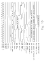
- FIG. 8 is a timing diagram illustrating signal states for a data mover read operation.
- FIG. 9 is a timing diagram illustrating signal states for interleaving a command executor read operation with a data mover read operation.
- FIG. 10 is a timing diagram illustrating signal states for interleaving a command executor write operation with a data mover read operation.
- the present invention provides a system and method for controlling a communications adapter interface such that supplemental data can be interleaved with data being transferred.
- the interleaving is performed in a manner such that the supplemental data is transparent to the data mover portion of the communications adapter.
- the supplemental data can be transferred in either read or write cycles that are interleaved at the beginning, in the middle, or at the end of data bursts or block data transfers.
- the interface bus is more fully utilized because arbitration and bus ownership changes do not create unused cycles.
- the interleaving is accomplished by temporarily halting an existing transfer of data and transferring the requested supplemental data while the original data transfer is halted. After the supplemental data is transferred, the transfer of the balance of the block of data originally being transferred is then allowed to continue. In other words, the present invention "steals" a cycle from the data transferror and uses this cycle to transfer supplemental data.
- a finite state machine controls the routine transfer of data between the master and the slave- device.
- the finite state machine is controlled to select which data is actually transferred and to which location.
- the data source, data direction, data addresses and read/write tags, of the finite state machine are changed thereby selecting whether data or supplemental data is transferred.
- a finite state machine is currently transferring data across a slave bus. If the finite state machine is transferring 21 bytes of data and it is desired to transfer a byte of supplemental data, the data address and data counters are inhibited from incrementing, and the addresses for the status byte are inserted so that the finite state machine actually transfers the status byte. Then, the address and counters are un-inhibited and the finite state machine transfers the balance of the 21 bytes of data. When the transfer is completed, the finite state machine will actually have sent 22 bytes of data.
- FIG. 1 illustrates just one example of such an environment in which the transparent interleaving according to the present invention can be implemented.
- a main processor 102 controls the operation of an HPPB bus 122.
- Other processors, and interface modules, although not shown, may also be connected to HPPB bus 122.
- a communications adapter 104 is provided to interface devices on HPPB bus 122 to a LAN controller 106.
- a communications channel 124 interfaces communications adapter 104 to LAN controller 106.
- communications channel 124 is a bus.
- LAN controller 106 controls the interface to a LAN 126.
- LAN 126 typically operates at a lower speed than HPPB bus 122.
- An example of a LAN 126 is a token ring.
- Communications adapter 104 is described in more detail with respect to FIG. 2.
- An example of a communications adapter 104 is the Foxburg Module and an example of LAN controller 106 is the Pinegrove Module. Both modules are available from International Business Machines (IBM) in Raleigh, North Carolina.
- FIG. 2 A functional block diagram of a communications adapter 104 is illustrated in FIG. 2.
- a picoprocessor 202 controls the operation of communications adapter 104.
- Picoprocessor 202 sets up all pointers and addresses necessary to transfer data between LAN controller 106 and main processor 102. Thus, instead of main processor 102 executing the details of a data transfer, picoprocessor 202 carries out these responsibilities.
- Data buffers 204 are used by picoprocessor 202 as a temporary store for the data to be transferred.
- An HPPB bus interface 206 provides an interface to HPPB bus 122.
- a communications channel interface 208 provides an interface to communications channel 124. Data is transferred among picoprocessor 202, data buffers 204, HPPB bus interface 206, and communications channel interface 208 using an internal bus 232.
- a scenario regarding how data is transferred using communications adapter 104 will first be described without discussion of the transparent interleaving.
- the scenario involves the process by which communications adapter 104 facilitates the operation of main processor 102 writing data to LAN controller 106.
- main processor 102 reads data from LAN controller 106 would be apparent to a person skilled in the relevant art.
- FIG. 3 is a flow diagram illustrating steps involved in this scenario.
- main processor 102 instructs picoprocessor 202 to send a frame of data.
- picoprocessor 202 receives this instruction and begins executing.
- picoprocessor 202 pulls the frame of data (or a subset thereof) from main processor 102 and stores it in data buffers 204. Picoprocessor 202 may manipulate the frame while it is in data buffers 204. Because communications adapter 104 operates at high speeds, the transfer of data over HPPB bus 122 to data buffers 204 occurs rapidly and does not consume an undue amount of HPPB bus time.
- picoprocessor 202 retrieves the data from data buffers 204 and sends it to LAN controller 106 via communications channel 124. Because LAN controller 106 operates at a slower rate than HPPB bus 122, this transfer is at a slower rate than that of the transfer in step 304. However, because this transfer involves only the communications channel 124 (and not HPPB bus 122) the performance of HPPB bus 122 is not impacted by the relatively slow speed of this operation.
- step 306 is asynchronous with respect to main processor 102 and HPPB bus 122.
- main processor 102 and HPPB bus 122 can perform other operations while the transfer of step 306 is taking place.
- Picoprocessor 202 performs the transfer of step 306 by incrementing counters and an address to transfer data from data buffers 204 to the correct destination.
- the operation of picoprocessor 202 in performing a routine data transfer between buffers and an I/O port is well known to persons skilled in the relevant art.
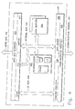
- FIG 4. is a functional block diagram illustrating a communications adapter 104 configured to allow such a transparent, interleaved transfer.
- a communications interface controller 420 controls the transfer of data and supplemental data between LAN controller 106 and communications adapter 104.
- Communications interface controller 420 comprises a data mover 422, a command executor 424 and a communications interface 426.
- data mover 422 is a finite state machine that performs the actual transfer of data.
- Command executor 424 handles supplemental data and "steals" cycles away from data mover 422 for transferring this supplemental data. The method by which this is accomplished is fully described below.
- a CE bus 434 is provided to transfer the supplemental data between an HPPB bus interface 410 and command executor 424.
- HPPB bus interface 410 can function as a master interface 414 or a slave interface 412 as illustrated in FIG. 4. When transfers are originated by main processor 102, communications adapter 104 is functioning as a slave and HPPB bus interface 410 is a slave interface 412. When transfers are originated by communications adapter 104 (or LAN controller 106), communications adapter 104 functions as the master and HPPB bus interface 410 is a master interface 414.
- FIG. 5 is a flow diagram illustrating the steps involved in an interleaved transfer.
- main processor 102 requests that a data transfer take place between itself and LAN controller 106. This data transfer is similar to the transfer described above with reference to FIG. 3. This transfer request is received by communications adapter 104.
- communications adapter 104 begins executing the data transfer requested in step 502.
- picoprocessor 202 retrieves data at high speed from main processor 102 via HPPB bus interface 410 and stores this data in data buffers 204. This data is then clocked out of data buffers and sent to LAN controller 106 over communications channel 124 via communications interface 426.
- picoprocessor retrieves data at slower speeds (relative to HPPB bus 122) from LAN controller 106 via communications interface 426 and stores this data in data buffers 204. This data is then sent to main processor 102 at high speed over the HPPB bus 122 via HPPB bus interface 410. Note, the read operation may be performed at the request of LAN controller 106 as opposed to main processor 102.
- Data mover 422 is a finite state machine that transfers one unit of data during each cycle. In a preferred embodiment the unit of data transferred is two bytes, or one half word. Data mover 422 uses addresses and counters to keep track of the data to be transferred at each cycle. At the end of each cycle the address and counters are incremented so that the next sequential unit of data is transferred. This continues until the balance of original block of data is transferred. The operation of data mover 422 in such a transfer is described in greater detail below with respect to the timing diagram in FIG. 8.
- An internal bus 432 is used to provide connectivity between HPPB bus interface 410, data buffers 204 and data mover 422. Data, address information, and supplemental data are transferred between HPPB bus interface 410, data buffers 204 and data mover 422.
- main processor 102 may determine that it needs to send supplemental data to LAN controller 106. In this case, main processor 102 sends this supplemental data to communications adapter 104 via HPPB bus 122. In a step 506, communications adapter 104 receives this supplemental data. More specifically slave HPPB bus interface 412 receives the information.
- Slave HPPB bus interface 412 puts this supplemental data onto CE bus 434 whereby it is transferred to command executor 424 in a step 508.
- Operations over CE bus 434 are asynchronous operations initiated by slave HPPB bus interface 412. These operations originate as either read or write operations to LAN controller 106 address space.
- command executor 424 receives the supplemental data and checks to see if data mover 422 is currently transferring data to LAN controller 106 (e.g., in step 504). If data mover 422 is not transferring data, CE bus 434 is connected to communications interface 426 and the transfer of supplemental data is executed in a step 512. If data mover 422 is currently transferring data over communications channel 124, the supplemental data transfer is controlled by communications interface controller 420 in a step 514.
- step 602 the current data transfer cycle (e.g., step 504) proceeds in a normal manner.
- a step 604 at the start of the next cycle (referred to as cycle N+1), CE bus 434 is connected to communications interface 426 and data mover 422 is disconnected.
- cycle N+1 is allocated to and taken by CE bus 434 (i.e., the cycle is stolen from data mover 422 by command executor 424).
- supplemental data is transferred to LAN controller 106 via communications interface 426 and communications channel 124.
- step 608 data mover's address counters and byte counters associated with the original data transfer (of step 504) are inhibited for one cycle.
- Data mover 422 executes cycle N+1 in a step 610. Because the counters are inhibited, they do not advance at the end of the cycle. Also, because data mover 422 is not connected to communications interface 426, the transfer of data that was originally supposed to take place during cycle N+1 does not occur.
- step 612 data mover 422 is reconnected to communications interface 426 and the data transfer operation resumes. Because the counters did not advance at the end of cycle N+1, the operation resumes with the transfer that was supposed to occur at cycle N+1.
- FIG. 7 is a block diagram illustrating communications interface controller 420. Referring to FIG. 7, communications interface controller 420 will now be described.
- a multiplexer 702 is used to select whether data to be transferred to LAN controller 106 is sourced from CE bus 434 or from interface register 706. Multiplexer 702 also selects the address and read/write signals from these two sources. If data to be transferred is supplemental data the data and address source is CE bus 434. If data to be transferred is data from data buffers 204, the source is internal bus 432.
- a data hold register 704 is used as a prefetch register to store prefetched data and addresses from internal bus 432.
- Data hold register 704 is used because internal bus 432 is a multiplexed bus and the data to be written to interface controller 106 is not always available. Therefore, data hold register 704 prefetches and stores the data when it is available. In this manner, the data is available to communications interface controller 420 when it is required.
- Data hold register 704 also holds data to be transmitted over internal bus 432.
- An interface register 706 retrieves the data from data hold register 704 so it is available at multiplexer 704.
- Control logic 708 is provided to perform logic functions such as parity checks and one byte or half word degating. Control logic 708 also determines whether data read from LAN controller 106 is supplemental data destined for CE bus 434 or data for internal bus 432. In this respect, control logic 708 performs a similar function for supplemental data reads that multiplexer 702 performs for supplemental data writes.
- Drivers and receivers 710 are provided to interface to communications channel 124. Drivers and receivers 710 provide the correct signal levels for transmission over communications channel 124.
- Communications channel 124 could be implemented using any of a variety of communications/protocol standards.
- One such standard is the IBM UC-5005 protocol.
- the UC-5005 protocol supports three modes of data transfer operations: basic, burst and byte.
- communications adapter 104 accesses LAN controller 106 in all three modes.
- the UC-5005 protocol interface signals are described in detail in Table 1. These signals describe communications channel 124 as implemented in a preferred embodiment. It will be apparent to a person skilled in the relevant art how communications channel 124 can be implemented using alternative protocols.
- Table 2 illustrates the signals used on CE bus 434 in a preferred embodiment. These signals are chosen to maximize utility in conjunction with the UC-5005 protocol used in communications channel 124. It will be apparent how a person skilled in the relevant art could use alternative signal implementations to achieve the goals of transferring supplemental data across CE bus 434 for transfer to/from LAN controller 106. Instead of MSEL as used in UC-5005, CE bus 434 uses a command executor start (CESTART) signal. CESTART indicates that HPPB slave interface 412 is requesting a command executor 422 transfer operation.
- CESTART command executor start
- CE bus signals include a command executor acknowledge signal (CEACK) that indicates to HPPB slave interface 412 that the requested transfer is completed.
- CEACK command executor acknowledge signal
- Address signals (CEADDOUT) provide the address of the space in LAN controller 106 to be used in the transfer.
- CE bus 434 uses three error signals to indicate three different types of errors.
- Command Executor Parity Check Error indicates whether the data received from LAN controller 106 has a parity error.
- the LAN controller error tag indicates that communications adapter 104 received an error tag from LAN controller 106.
- the command executor error tag indicates that LAN controller 106 failed to respond to communications adapter 104.
- Table 3 lists and describes the signals used on internal bus 432 in a preferred embodiment.
- each user has a dedicated address.
- DMBID data mover bid signal
- DMSEL data mover select signal
- FIG. 8 is a timing diagram illustrating a read operation of communications adapter 104. More specifically, Figure 8 illustrates signals associated with a read operation of data mover 422.
- a B-clock signal (B Clk) 802 launches data onto internal bus 432. This data is latched using a C-clock signal (C Clk) 804. The cycle is measured from one rising edge of B Clk 802 to the next rising edge of B Clk 802.
- a start data mover signal (SDM) 806 tells data mover 422 to start transferring data.
- SDM 806 is set by picoprocessor 202.
- SDM 806 is not set positive until all of the address pointers and read/write signals have been set to the correct state.
- Write signal 808 is an active low signal that goes high for a read operation. Because FIG. 8 illustrates a read operation, Write signal 808 is illustrated high. During write operations, write signal 808 is at a low level.
- HWD 810 is the active half-word bus transfer signal. When HWD 810 is not positive, this indicates a half-word transfer as opposed to a full-word transfer.
- Write signal 808 and HWD 810 are set by picoprocessor 202.
- CESTART 812 is a signal from command executor 422 indicating that supplemental data is to be transferred. CESTART 812 is positive when command executor 422 has supplemental data to be transferred. If CESTART 812 goes positive when data is being transferred by data mover 422, this indicates that supplemental data is to be interleaved with data currently being transferred.
- Read FSM 814 indicates which of four states the finite state machine is in. It is in state R1 that the finite state machine in data mover 422 transfers data to LAN controller 106.
- MSEL 816 goes low to indicate that a memory mapped I/O transfer has been selected. This signal, on communications channel 124, indicates that a transfer between LAN controller 106 and communications adapter 104 is to take place.
- MSEL 816 is a synchronization signal between communications adapter 104 and LAN controller 106. communications adapter 104 activates MSEL 816 to indicate to LAN controller 106 that everything is ready for a data transfer operation.
- MUXDM 818 controls multiplexer 702.
- a positive MUXDM 818 signal controls multiplexer 702 to select data from data mover 422.
- Transfer acknowledge signal XFERACK 820 transitions to negative to indicate that LAN controller 106 has received the transferred data. This is an acknowledge signal from LAN controller 106 over communications channel 124.
- ACK 822 is a latched version of XFERACK 820.
- ACK 822 is the opposite polarity of XFERACK 820.
- LAN controller 106 Once LAN controller 106 has received or supplied the data for the transfer, it responds by activating XFERACK 820 which is latched to form ACK 822.
- communications adapter 104 receives XFERACK 820, the operation is completed and MSEL 816 is deactivated.
- MSEL 816 When LAN controller 104 sees that MSEL 816 is not active, it deactivates XFERACK 820. This "hand shaking" is repeated for every half word (two bytes) of data that are transferred.
- Set bid signal 824 is the signal used by data mover 422 to request access to communications channel 124.
- Set bid signal 824 is latched to form latched bid signal 826.
- select signal 828 When data mover 422 is granted access to the bus, select signal 828 is positive. Select signal 828 is latched to form latched select signal 830. A positive select signal 828 indicates to data mover 422 that it has the bus on the following cycle.
- Internal address 832 is the address for data buffers 204.
- Figure 9 is a timing diagram illustrating a command executor read cycle interleaved within a data mover read operation.
- the signals illustrated in Figure 9 are essentially the same as those in Figure 8. Some additional signals are illustrated for the command executor read cycle.
- Start data mover 806 is activated indicating that a data mover transfer is in process.
- Write signal 808 is activated indicating that the data mover transfer is a read operation versus a write operation.
- HWD 810 is active indicating a half word transfer.
- CESTART signal 812 goes active when command executor 422 wishes to interrupt the data mover cycle and interleave supplemental data. This is illustrated by the positive transition of CESTART signal 812 in Figure 9.
- the CE cycle will be interleaved within the data mover transfer. If the amount of remaining data bytes to transfer is 4 or more, if there is no error, and if there is no request to abort the operation, then the read finite state machine checks for an active CESTART 812 signal during the R1 state. If, at this time, CESTART 812 is active and ACK 822 has been set, multiplexer 702 is switched to accept data from command executor 422. This is indicated by MUXDM signal 818 in the negative state. This action changes the LAN controller 104 address 834 and data signals to contain the information provided by command executor 422. As illustrated in Figure 9, HW signal 910 may change depending on whether the CE transfer is a half-word transfer. Write signal 908 does not go low because the CE operation interleaved is a read cycle.
- Figure 9 also illustrates LAN control address 834 and the portion of that address 934 that contains the address for a command executor read cycle. Note, there is no bid for internal bus 432 while the command executor cycle is being serviced as this cycle uses dedicated CE bus 434. Also note that internal address 832 will not be incremented during the cycle in which the command executor cycle occurs.
- LAN controller address 834 is incremented when the finite state machine transitions out of state R1. Also at this time, multiplexer 702 is switched back to servicing data mover 422 as illustrated by the positive transition of MUXDM signal 818 in Figure 9. If multiplexer 802 switches at a rate slower than the time it takes for the counters containing LAN controller address 834 to increment, LAN controller address signals 834 will show a double change. This, however, has no adverse impact because LAN controller address signal 834 has sufficient time to stabilize before MSEL 816 is activated (negative) and LAN controller 106 uses the address.
- Figure 10 is a timing diagram illustrating a command executor write signal interleaved within a data mover read operation.
- the command executor cycle to be serviced is a write operation and the data mover operation is a read operation
- drivers/receivers 710 must be "turned around” because they are currently in the receiver mode.
- Figure 10 illustrates set driver enable signal 1002 and the latched version of this signal, data driver signal 1004.
- set driver enable signal 1002 is positive and this signal is latched
- the data drivers will be enabled for a write operation.
- These are data drivers of communications adapter 104. These drivers must be switched off rapidly once the transfer is complete and WRTL 908 has changed, in order to avoid collisions with LAN controller 106 drivers.
- data drivers signal 1004 is gated by write signal 908. As soon as write signal 908 changes, the drivers are disabled.
- Write signal 908 goes active during the time that command executor 422 is granted access to communications channel 124. This is not the case for the read operation described with reference to FIG. 9.
Landscapes
- Engineering & Computer Science (AREA)
- Theoretical Computer Science (AREA)
- Physics & Mathematics (AREA)
- General Engineering & Computer Science (AREA)
- General Physics & Mathematics (AREA)
- Bus Control (AREA)
- Computer And Data Communications (AREA)
- Communication Control (AREA)
Applications Claiming Priority (2)
| Application Number | Priority Date | Filing Date | Title |
|---|---|---|---|
| US08/040,317 US5535333A (en) | 1993-03-30 | 1993-03-30 | Adapter for interleaving second data with first data already transferred between first device and second device without having to arbitrate for ownership of communications channel |
| US40317 | 1993-03-30 |
Publications (2)
| Publication Number | Publication Date |
|---|---|
| EP0618537A1 true EP0618537A1 (fr) | 1994-10-05 |
| EP0618537B1 EP0618537B1 (fr) | 2000-04-26 |
Family
ID=21910342
Family Applications (1)
| Application Number | Title | Priority Date | Filing Date |
|---|---|---|---|
| EP94480012A Expired - Lifetime EP0618537B1 (fr) | 1993-03-30 | 1994-02-22 | Système et procédé d'entrelacement d'information d'état avec transferts de données dans un adaptateur de communication |
Country Status (4)
| Country | Link |
|---|---|
| US (1) | US5535333A (fr) |
| EP (1) | EP0618537B1 (fr) |
| JP (1) | JP2688171B2 (fr) |
| DE (1) | DE69424083D1 (fr) |
Families Citing this family (12)
| Publication number | Priority date | Publication date | Assignee | Title |
|---|---|---|---|---|
| JPH10254798A (ja) * | 1997-03-12 | 1998-09-25 | Mitsubishi Electric Corp | Mmi通信装置 |
| US6085285A (en) * | 1997-11-13 | 2000-07-04 | International Business Machines Corporation | Intermixing different devices along a single data communication link by placing a strobe signal in a parity bit slot |
| US6434650B1 (en) | 1998-10-21 | 2002-08-13 | Intel Corporation | Apparatus and method for multiplexing bi-directional data onto a low pin count bus between a host CPU and co-processor |
| US6463494B1 (en) | 1998-12-30 | 2002-10-08 | Intel Corporation | Method and system for implementing control signals on a low pin count bus |
| JP4010718B2 (ja) * | 1999-10-29 | 2007-11-21 | ローム株式会社 | データ転送方式 |
| US6775727B2 (en) * | 2001-06-23 | 2004-08-10 | Freescale Semiconductor, Inc. | System and method for controlling bus arbitration during cache memory burst cycles |
| US7398446B2 (en) * | 2003-05-29 | 2008-07-08 | Lucent Technologies Inc. | Low power operation of an address interleaver |
| US7013357B2 (en) * | 2003-09-12 | 2006-03-14 | Freescale Semiconductor, Inc. | Arbiter having programmable arbitration points for undefined length burst accesses and method |
| US8402233B2 (en) * | 2005-09-07 | 2013-03-19 | Broadcom Corporation | Method and apparatus for high throughput mass storage device interface in a microprocessor for handheld systems |
| KR100871853B1 (ko) * | 2006-06-05 | 2008-12-03 | 삼성전자주식회사 | 비압축 av 데이터 전송을 위한 데이터 슬롯 할당 방법,비압축 av 데이터 전송 방법, 및 상기 방법을 이용하는장치 |
| WO2016182743A1 (fr) | 2015-05-09 | 2016-11-17 | Medtronic, Inc. | Procédés et dispositifs utilisant un matériel pour déplacer des blocs de données de paramètres de fonctionnement d'une mémoire à un ensemble de registres |
| US11216370B2 (en) * | 2018-02-20 | 2022-01-04 | Medtronic, Inc. | Methods and devices that utilize hardware to move blocks of operating parameter data from memory to a register set |
Citations (2)
| Publication number | Priority date | Publication date | Assignee | Title |
|---|---|---|---|---|
| EP0428330A2 (fr) * | 1989-11-13 | 1991-05-22 | International Business Machines Corporation | Circuit interface de calculateur |
| EP0530543A1 (fr) * | 1991-08-12 | 1993-03-10 | Stratus Computer, Inc. | Dispositif et méthode de commande d'entrées/sorties pour le transfert de données entre un processeur hôte et plusieurs unités entrées/sorties |
Family Cites Families (6)
| Publication number | Priority date | Publication date | Assignee | Title |
|---|---|---|---|---|
| JPS5892025A (ja) * | 1981-11-26 | 1983-06-01 | Hitachi Ltd | デ−タ処理方式 |
| US5142689A (en) * | 1982-09-27 | 1992-08-25 | Siemens Nixdort Informationssysteme Ag | Process for the preparation of the connection of one of several data processor devices to a centrally synchronized multiple line system |
| US5019966A (en) * | 1986-09-01 | 1991-05-28 | Nec Corporation | Dual processors using busy signal for controlling transfer for predetermined length data when receiving processor is processing previously received data |
| US5109501A (en) * | 1986-10-13 | 1992-04-28 | Matsushita Electric Industrial Co., Ltd. | Data transfer apparatus having a transferable data counter |
| JPH03263953A (ja) * | 1990-03-14 | 1991-11-25 | Hitachi Ltd | ターミナルアダプタ |
| JPH03269659A (ja) * | 1990-03-19 | 1991-12-02 | Nec Corp | マイクロプロセッサ |
-
1993
- 1993-03-30 US US08/040,317 patent/US5535333A/en not_active Expired - Fee Related
-
1994
- 1994-02-22 DE DE69424083T patent/DE69424083D1/de not_active Expired - Lifetime
- 1994-02-22 EP EP94480012A patent/EP0618537B1/fr not_active Expired - Lifetime
- 1994-03-02 JP JP6032495A patent/JP2688171B2/ja not_active Expired - Fee Related
Patent Citations (2)
| Publication number | Priority date | Publication date | Assignee | Title |
|---|---|---|---|---|
| EP0428330A2 (fr) * | 1989-11-13 | 1991-05-22 | International Business Machines Corporation | Circuit interface de calculateur |
| EP0530543A1 (fr) * | 1991-08-12 | 1993-03-10 | Stratus Computer, Inc. | Dispositif et méthode de commande d'entrées/sorties pour le transfert de données entre un processeur hôte et plusieurs unités entrées/sorties |
Also Published As
| Publication number | Publication date |
|---|---|
| JP2688171B2 (ja) | 1997-12-08 |
| DE69424083D1 (de) | 2000-05-31 |
| EP0618537B1 (fr) | 2000-04-26 |
| US5535333A (en) | 1996-07-09 |
| JPH08167921A (ja) | 1996-06-25 |
Similar Documents
| Publication | Publication Date | Title |
|---|---|---|
| US5301279A (en) | Apparatus for conditioning priority arbitration | |
| US5444853A (en) | System and method for transferring data between a plurality of virtual FIFO's and a peripheral via a hardware FIFO and selectively updating control information associated with the virtual FIFO's | |
| EP0489504B1 (fr) | Tampon FIFO bidirectionnel pour réaliser l'interfaçage entre deux barres omnibus | |
| US6151651A (en) | Communication link with isochronous and asynchronous priority modes coupling bridge circuits in a computer system | |
| EP1047994B1 (fr) | Interface de bus de donnees intelligente dans laquelle une memoire a acces multiples est utilisee | |
| US8156270B2 (en) | Dual port serial advanced technology attachment (SATA) disk drive | |
| US7096296B2 (en) | Supercharge message exchanger | |
| US4937734A (en) | High speed bus with virtual memory data transfer and rerun cycle capability | |
| US6148357A (en) | Integrated CPU and memory controller utilizing a communication link having isochronous and asynchronous priority modes | |
| US5121487A (en) | High speed bus with virtual memory data transfer capability using virtual address/data lines | |
| US20090177815A1 (en) | Switching serial advanced technology attachment (sata) to a parallel interface | |
| US20090177804A1 (en) | Serial advanced technology attachment (sata ) switch | |
| US6636927B1 (en) | Bridge device for transferring data using master-specific prefetch sizes | |
| US6889266B1 (en) | Method for delivering packet boundary or other metadata to and from a device using direct memory controller | |
| EP0618537B1 (fr) | Système et procédé d'entrelacement d'information d'état avec transferts de données dans un adaptateur de communication | |
| EP0535793B1 (fr) | Méthode pour conduire des transferts de données dans un système d'ordinateur avec une structure à double bus | |
| KR20010024260A (ko) | 핀-총수가 적은 버스 상에서의 직접 메모리 억세스 트랜잭션 | |
| CN114662136A (zh) | 一种基于pcie通道的多算法ip核的高速加解密系统及方法 | |
| US6401142B1 (en) | Apparatus and method for selective bus transfer using master and slave modes | |
| US6157971A (en) | Source-destination re-timed cooperative communication bus | |
| US5911152A (en) | Computer system and method for storing data in a buffer which crosses page boundaries utilizing beginning and ending buffer pointers | |
| US5097483A (en) | Tri-statable bus with apparatus to drive bus line to first level and then second level for predetermined time before turning off | |
| JP4903801B2 (ja) | FlexRay通信モジュールとFlexRay加入者装置とを繋ぐ加入者インタフェース、およびFlexRay通信モジュールとFlexRay加入者装置とを繋ぐ加入者インタフェースを経由するメッセージの伝送方法 | |
| JP3703532B2 (ja) | 多重化アドレスバスを備えたコンピュータシステム | |
| JPH08314854A (ja) | データ転送システムおよびこれに関連する装置 |
Legal Events
| Date | Code | Title | Description |
|---|---|---|---|
| PUAI | Public reference made under article 153(3) epc to a published international application that has entered the european phase |
Free format text: ORIGINAL CODE: 0009012 |
|
| AK | Designated contracting states |
Kind code of ref document: A1 Designated state(s): DE FR GB |
|
| 17P | Request for examination filed |
Effective date: 19950117 |
|
| 17Q | First examination report despatched |
Effective date: 19980408 |
|
| GRAG | Despatch of communication of intention to grant |
Free format text: ORIGINAL CODE: EPIDOS AGRA |
|
| GRAG | Despatch of communication of intention to grant |
Free format text: ORIGINAL CODE: EPIDOS AGRA |
|
| GRAH | Despatch of communication of intention to grant a patent |
Free format text: ORIGINAL CODE: EPIDOS IGRA |
|
| GRAH | Despatch of communication of intention to grant a patent |
Free format text: ORIGINAL CODE: EPIDOS IGRA |
|
| GRAA | (expected) grant |
Free format text: ORIGINAL CODE: 0009210 |
|
| AK | Designated contracting states |
Kind code of ref document: B1 Designated state(s): DE FR GB |
|
| PG25 | Lapsed in a contracting state [announced via postgrant information from national office to epo] |
Ref country code: FR Free format text: LAPSE BECAUSE OF FAILURE TO SUBMIT A TRANSLATION OF THE DESCRIPTION OR TO PAY THE FEE WITHIN THE PRESCRIBED TIME-LIMIT Effective date: 20000426 |
|
| REF | Corresponds to: |
Ref document number: 69424083 Country of ref document: DE Date of ref document: 20000531 |
|
| PG25 | Lapsed in a contracting state [announced via postgrant information from national office to epo] |
Ref country code: DE Free format text: LAPSE BECAUSE OF FAILURE TO SUBMIT A TRANSLATION OF THE DESCRIPTION OR TO PAY THE FEE WITHIN THE PRESCRIBED TIME-LIMIT Effective date: 20000727 |
|
| EN | Fr: translation not filed | ||
| PLBE | No opposition filed within time limit |
Free format text: ORIGINAL CODE: 0009261 |
|
| STAA | Information on the status of an ep patent application or granted ep patent |
Free format text: STATUS: NO OPPOSITION FILED WITHIN TIME LIMIT |
|
| 26N | No opposition filed | ||
| REG | Reference to a national code |
Ref country code: GB Ref legal event code: IF02 |
|
| PGFP | Annual fee paid to national office [announced via postgrant information from national office to epo] |
Ref country code: GB Payment date: 20030203 Year of fee payment: 10 |
|
| PG25 | Lapsed in a contracting state [announced via postgrant information from national office to epo] |
Ref country code: GB Free format text: LAPSE BECAUSE OF NON-PAYMENT OF DUE FEES Effective date: 20040222 |
|
| GBPC | Gb: european patent ceased through non-payment of renewal fee |
Effective date: 20040222 |