EP0618747A2 - Steuerbare optische Verzögerungsleitung - Google Patents
Steuerbare optische Verzögerungsleitung Download PDFInfo
- Publication number
- EP0618747A2 EP0618747A2 EP94301897A EP94301897A EP0618747A2 EP 0618747 A2 EP0618747 A2 EP 0618747A2 EP 94301897 A EP94301897 A EP 94301897A EP 94301897 A EP94301897 A EP 94301897A EP 0618747 A2 EP0618747 A2 EP 0618747A2
- Authority
- EP
- European Patent Office
- Prior art keywords
- waveguides
- input
- wavelength
- output
- optical
- Prior art date
- Legal status (The legal status is an assumption and is not a legal conclusion. Google has not performed a legal analysis and makes no representation as to the accuracy of the status listed.)
- Granted
Links
Images

Classifications
-
- G—PHYSICS
- G02—OPTICS
- G02B—OPTICAL ELEMENTS, SYSTEMS OR APPARATUS
- G02B6/00—Light guides; Structural details of arrangements comprising light guides and other optical elements, e.g. couplings
- G02B6/10—Light guides; Structural details of arrangements comprising light guides and other optical elements, e.g. couplings of the optical waveguide type
- G02B6/12—Light guides; Structural details of arrangements comprising light guides and other optical elements, e.g. couplings of the optical waveguide type of the integrated circuit kind
- G02B6/12007—Light guides; Structural details of arrangements comprising light guides and other optical elements, e.g. couplings of the optical waveguide type of the integrated circuit kind forming wavelength selective elements, e.g. multiplexer, demultiplexer
- G02B6/12009—Light guides; Structural details of arrangements comprising light guides and other optical elements, e.g. couplings of the optical waveguide type of the integrated circuit kind forming wavelength selective elements, e.g. multiplexer, demultiplexer comprising arrayed waveguide grating [AWG] devices, i.e. with a phased array of waveguides
- G02B6/12019—Light guides; Structural details of arrangements comprising light guides and other optical elements, e.g. couplings of the optical waveguide type of the integrated circuit kind forming wavelength selective elements, e.g. multiplexer, demultiplexer comprising arrayed waveguide grating [AWG] devices, i.e. with a phased array of waveguides characterised by the optical interconnection to or from the AWG devices, e.g. integration or coupling with lasers or photodiodes
- G02B6/12021—Comprising cascaded AWG devices; AWG multipass configuration; Plural AWG devices integrated on a single chip
-
- G—PHYSICS
- G02—OPTICS
- G02B—OPTICAL ELEMENTS, SYSTEMS OR APPARATUS
- G02B6/00—Light guides; Structural details of arrangements comprising light guides and other optical elements, e.g. couplings
- G02B6/24—Coupling light guides
- G02B6/26—Optical coupling means
- G02B6/28—Optical coupling means having data bus means, i.e. plural waveguides interconnected and providing an inherently bidirectional system by mixing and splitting signals
- G02B6/2804—Optical coupling means having data bus means, i.e. plural waveguides interconnected and providing an inherently bidirectional system by mixing and splitting signals forming multipart couplers without wavelength selective elements, e.g. "T" couplers, star couplers
- G02B6/2861—Optical coupling means having data bus means, i.e. plural waveguides interconnected and providing an inherently bidirectional system by mixing and splitting signals forming multipart couplers without wavelength selective elements, e.g. "T" couplers, star couplers using fibre optic delay lines and optical elements associated with them, e.g. for use in signal processing, e.g. filtering
-
- H—ELECTRICITY
- H04—ELECTRIC COMMUNICATION TECHNIQUE
- H04Q—SELECTING
- H04Q11/00—Selecting arrangements for multiplex systems
- H04Q11/0001—Selecting arrangements for multiplex systems using optical switching
- H04Q11/0003—Details
Definitions
- This invention relates to optical communications system. More particularly, this invention relates to optical delay lines which are variable and can be used in optical communications systems.
- variable optical delay line has been developed.
- the variable delay line in accordance with this invention may be based upon photonic integrated circuitry which can provide a large range of time delay to an optical signal, and this can be realized at a relatively low cost.
- the inventors have realized that integrated optical devices disclosed, for example, in U.S. Patents 5,002,350 and 5,136,671 may be used to create a variable optical delay line having a wide range of delays.
- the invention which is here disclosed comprises two identical 1 ⁇ N wavelength routing devices interconnected with optical waveguides. Each of the interconnecting optical waveguides has a specific length which is different from the length of the other waveguides.
- the 1 ⁇ N wavelength routing device connected to receive the incoming optical signal which is to be delayed can be considered to have at least one input port and a plurality of output ports where a signal of a specific wavelength that is received by the input port will be directed to a specific one of the plurality of output ports. In operation, it is the wavelength of the input signal that determines which one of the output ports will receive the input signal.
- a wavelength shifter is coupled to the input waveguide of the first or input wavelength routing device to shift the wavelength of a received optical signal to another wavelength.
- the received optical signal is directed by the input wavelength routing device to a specific one of the interconnecting optical waveguides, and, therefore, to a waveguide of a specific length which provides the desired controllable delay.
- the second wavelength routing device directs optical signals from each of the various optical waveguides of different lengths to a common output waveguide.
- a second wavelength shifter can be connected to the common output waveguide of the second wavelength routing device to shift the optical output signal back to its original wavelength.
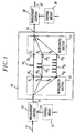
- FIG. 1 illustrates an example of a variable optical delay line which can provide a wide range of delays in accordance with the principles of the invention.
- the variable delay line is composed of two frequency routing devices, interconnected with optical waveguides of different lengths and a controllable wavelength shifter at the input of the device. These structures may be monolithically integrated either partially or fully on a semiconductive wafer and formed by means of known photolithographic techniques.
- the delays which are obtainable are limited by the size of the wafer. More delay flexibility is obtainable by using a partially integrated structure where optical fibers are used for obtaining the delay.
- FIG. 1 illustrates a wafer 10 made of a semiconductive material such as an indium phosphide based material such as InGaAsP.
- An optical signal of a known wavelength is directed via an input optical waveguide 11 to a wavelength shifter 13 which shifts the frequency of the received optical signal from its received wavelength to a second wavelength.
- the optical wavelength signal from the wavelength shifter is carried by waveguide 14 to a first input wavelength router 12 defined on the wafer 10.
- the wavelength router 12 may receive N input optical wavelengths F1,F2, ... F N on the single input waveguide 14 defined on wafer 10.
- the first wavelength router 12 receives and directs the input optical wavelength to an appropriate output port 161,162, ... 16 N of the wavelength router 12.
- a signal of wavelength F1 received by input waveguide 14 is directed to the output port 161,
- a signal of wavelength F2 is directed to the output port 162, and so on up to a signal of wavelength F N which is directed to output port 16 N .
- Each of the output ports 161,162, ... 16 N is connected to an appropriate input port 201,202, ... 20 N of a second wavelength router 20 via waveguides 181,182, ... 18 N of unequal lengths.
- the waveguides 181,182, ... 18 N of unequal lengths provide a predetermined amount of path length difference to the optical signals from the different output ports 161,162, ...16 N and, therefore, these waveguides provide different time delays to signals that they carry.
- the waveguides 181,182, ... 18 N can be formed on the wafer 10 by selectively doping narrow elongated portions of the wafer or they can be various lengths of individual optical fibers.
- the details of creating such waveguides in a wafer such as the indium phosphide wafer 10 illustrated in FIG. 1 are generally known and are not a part of this invention. Thus, they are not described here.
- a signal of a first wavelength received on waveguide 11 is shifted to a signal of a second wavelength by wavelength shifter 13.
- the wavelength shift that is applied to the received optical signal determines the path that the signal takes in going through the wavelength routers 12, 22 and the waveguides 181,182, ... 18 N and, therefore, the amount of delay that the signal will experience.
- the wavelength signal on waveguide 11 may be shifted over a 50nm bandwidth in the 1.5 ⁇ m region.
- a wavelength shifter suitable for shifting a wavelength signal is disclosed in the Electronics Letters', 27th August, 1992, Vol. 28, No. 18, by B.
- the wavelength shifter disclosed in this publication is based on the gain-saturation effect in a semiconductor optical amplifier. It can transfer multigigabit data streams between two or more wavelengths, tunable over a 50 nm bandwidth in the 1.5 ⁇ m region. It also provides conversion gain and is cascadable, while causing negligible signal degradation.
- the disclosed wavelength shifter provides a shift in wavelength by copying data onto signals at different wavelengths. Data copying is based on the well-known gain saturation induced cross-talk effect which is usually avoided as a nuisance in conventional optical amplification, but carried to its extreme in this instance. The use of this effects limits the modulation format to digital intensity modulation. Within this constraint, the result is the same as a wavelength shift.
- the wavelength shifter 13 is coupled via input waveguide 14 to the first wavelength router 12.
- the path of the wavelength signal through the first wavelength router 12 is determined by the wavelength of the signal on waveguide 14.
- an input signal of wavelength F1 on waveguide 14 is directed by wavelength router 12 to output port 161
- an input signal of wavelength F2 is directed to output port 162
- so on up to an input signal of wavelength of F N which is directed to output port 16 N .
- Each of the output ports 161,162, ... 16 N is connected to an optical waveguide which has a different predetermined length.
- an optical signal that is to have a long delay is directed to an optical waveguide that is relatively long such as waveguide 18 N while an optical signal that is to have a shorter delay is directed to an optical waveguide that is relatively shorter such as waveguide 182.
- output port 161 is connected to the input of a waveguide 181 of a first length
- output port 162 is connected to the input of a waveguide 182 of a second length which is longer than waveguide 181, and so on up to output port 16 N which is connected to the input of a waveguide 18 N of a length which is a waveguide of the longest length.
- the outputs of the waveguides 181,182, ... 18 N are connected to respective input ports 201, 202, ... 20 N of a second frequency router 22.
- Frequency router 22 redirects the signal which appears at the N input ports 201,202,...20 N onto a single output waveguide 24.
- a second wavelength shifter 26, which is controlled by control means 28, can be connected to shift the wavelength of the signal on the output waveguide 24 back to the wavelength of the signal initially received on input optical waveguide 11.
- the path 181,182, ... 18 N that the signal takes in going from the first or input wavelength router 12 to the output wavelength router 22 is determined by the wavelength of the signal.
- the time that it takes for a signal to travel from the input waveguide 11 to the output waveguide 27 is determined by the wavelength of the signal from the wavelength shifter 13.
- the time delay that a signal experiences is going from an input waveguide to an output waveguide is controlled by controlling the wavelength of the signal.
- FIG. 2 shows the pertinent details of the wavelength routers 12 and 22 illustrated in FIG. 1.
- the wavelength routers may have identical configurations.
- Each wavelength routers contains a plurality of input ports 26 connected via input waveguides to a free region 28.
- a plurality of output ports 30 connected to waveguides extend from the free space region 28 and is connected to an optical grating 32.
- the optical grating 32 comprises a plurality of unequal length waveguides which provides a predetermined amount of path length difference to a corresponding plurality of input ports 34 connected to waveguides connected to another free space region 36.
- the free space region 36 is connected to a plurality of output ports 38 connected to waveguides 39.
- Patents 5,002,350 and 5,136,671 the entire contents of which are hereby incorporated by reference into this application.
- one of the input ports 26 is connected to the input waveguide 14 of the device shown in FIG. 1, and the plurality of waveguides 39 connected to output ports 38 are used as the output ports 161,162, ... 16 N .
- the plurality of input ports 26 connected to waveguides are the input ports 201,202, ... 20 N shown in FIG. 1 and one of the output waveguides 39 is the output waveguide 24 shown in FIG. 1.
- the device of FIG. 1 may be tuned to a large number of different optical wavelengths used in high speed, high capacity optical communications networks. For example, frequency routing devices where N is equal to 32 or more may be conveniently fabricated on a single semiconductive wafer. In accordance with the principles of this invention, this results in an optical delay line which can provide up to 32 or more different delays to a received signal.
Landscapes
- Physics & Mathematics (AREA)
- Engineering & Computer Science (AREA)
- General Physics & Mathematics (AREA)
- Optics & Photonics (AREA)
- Signal Processing (AREA)
- Theoretical Computer Science (AREA)
- Computer Networks & Wireless Communication (AREA)
- Microelectronics & Electronic Packaging (AREA)
- Optical Communication System (AREA)
- Optical Integrated Circuits (AREA)
Applications Claiming Priority (2)
| Application Number | Priority Date | Filing Date | Title |
|---|---|---|---|
| US38589 | 1993-03-26 | ||
| US08/038,589 US5367586A (en) | 1993-03-26 | 1993-03-26 | Optical delay line |
Publications (3)
| Publication Number | Publication Date |
|---|---|
| EP0618747A2 true EP0618747A2 (de) | 1994-10-05 |
| EP0618747A3 EP0618747A3 (de) | 1995-08-02 |
| EP0618747B1 EP0618747B1 (de) | 2003-01-08 |
Family
ID=21900772
Family Applications (1)
| Application Number | Title | Priority Date | Filing Date |
|---|---|---|---|
| EP94301897A Expired - Lifetime EP0618747B1 (de) | 1993-03-26 | 1994-03-16 | Steuerbare optische Verzögerungsleitung |
Country Status (4)
| Country | Link |
|---|---|
| US (1) | US5367586A (de) |
| EP (1) | EP0618747B1 (de) |
| JP (1) | JP3660367B2 (de) |
| DE (1) | DE69431973T2 (de) |
Cited By (6)
| Publication number | Priority date | Publication date | Assignee | Title |
|---|---|---|---|---|
| FR2725528A1 (fr) * | 1994-10-11 | 1996-04-12 | Alcatel Nv | Ligne a retard optique selectif en longueur d'onde |
| WO1996036858A3 (en) * | 1995-05-15 | 1997-02-13 | Tracor | High spectral resolution fiber optic spectrometer |
| WO1998028874A1 (en) * | 1996-12-23 | 1998-07-02 | Dsc Communications A/S | A bidirectional router and a method of monodirectional amplification |
| WO2002076000A1 (en) * | 2001-03-19 | 2002-09-26 | General Instrument Corporation | Time slot tunable all-optical packet data demultiplexer |
| EP1111955A3 (de) * | 1999-12-23 | 2007-08-08 | Lucent Technologies Inc. | Stringente Blockierungsfreie Wellenlängenmultiplexierte Querverbindungseinrichtung zur Verwendung in einem netzwerk |
| GB2474863A (en) * | 2009-10-28 | 2011-05-04 | Univ Gent | Optical buffer with controllable delay |
Families Citing this family (41)
| Publication number | Priority date | Publication date | Assignee | Title |
|---|---|---|---|---|
| EP0612164A1 (de) * | 1993-02-19 | 1994-08-24 | AT&T Corp. | Schnell abstimmbarer breitbandiger intergrierter optischer Filter |
| DE69523104T2 (de) * | 1994-02-11 | 2002-06-06 | Koninklijke Philips Electronics N.V., Eindhoven | Phasengekoppelte optische vorrichtung |
| US5524014A (en) * | 1994-05-23 | 1996-06-04 | At&T Corp. | Optical frequency translator |
| US5488680A (en) * | 1994-08-24 | 1996-01-30 | At&T Corp. | Frequency routing device having a wide and substantially flat passband |
| US5488500A (en) * | 1994-08-31 | 1996-01-30 | At&T Corp. | Tunable add drop optical filtering method and apparatus |
| US5467418A (en) * | 1994-09-02 | 1995-11-14 | At&T Ipm Corp. | Frequency routing device having a spatially filtered optical grating for providing an increased passband width |
| US5600742A (en) * | 1994-09-30 | 1997-02-04 | Lucent Technologies Inc. | Wavelength grating router with output coupler |
| US5566014A (en) * | 1994-12-28 | 1996-10-15 | At&T Corp. | Tunable add/drop optical filter providing arbitrary channel arrangements |
| FR2743234B1 (fr) * | 1995-12-28 | 1998-01-23 | Alcatel Optronics | Demultiplexeur de longueurs d'onde |
| US5841583A (en) * | 1996-02-09 | 1998-11-24 | Corning Incorporated | Multi-path interference filter |
| US6046854A (en) * | 1996-02-09 | 2000-04-04 | Corning Incorporated | Multi-path interference filter with reflective surfaces |
| US5793907A (en) * | 1996-03-28 | 1998-08-11 | The Regents Of The University Of California | Method and apparatus for a wavelength selective true-time delay for an optically controlled device |
| US5895775A (en) * | 1996-04-19 | 1999-04-20 | Trw Inc. | Microwave grating for dispersive delay lines having non-resonant stubs spaced along a transmission line |
| US5838851A (en) * | 1996-06-24 | 1998-11-17 | Trw Inc. | Optical-loop signal processing using reflection mechanisms |
| JPH1093164A (ja) | 1996-09-17 | 1998-04-10 | Kokusai Denshin Denwa Co Ltd <Kdd> | 多波長光源及び離散波長可変光源 |
| US5701372A (en) * | 1996-10-22 | 1997-12-23 | Texas Instruments Incorporated | Hybrid architecture for integrated optic switchable time delay lines and method of fabricating same |
| US5745616A (en) * | 1996-11-27 | 1998-04-28 | Lucent Technologies Inc. | Waveguide grating router and method of making same having relatively small dimensions |
| US6025944A (en) * | 1997-03-27 | 2000-02-15 | Mendez R&D Associates | Wavelength division multiplexing/code division multiple access hybrid |
| US6285477B1 (en) * | 1997-09-17 | 2001-09-04 | Kokusai Denshin Denwa Kabushiki Kaisha | Multi-wavelength light source and discrete-wavelength-variable light source |
| GB2334594A (en) * | 1998-02-20 | 1999-08-25 | Fujitsu Telecommunications Eur | Arrayed waveguide grating device |
| US5917970A (en) * | 1998-04-21 | 1999-06-29 | The United States Of America As Represented By The Secretary Of The Navy | Wavelength multiplexed, electro-optically controllable, fiber optic multi-tap delay line |
| US6160930A (en) * | 1998-08-11 | 2000-12-12 | Trw Inc. | Optical sample and hold architecture |
| US6567197B1 (en) * | 1998-10-20 | 2003-05-20 | At&T Corp. | Optical ring network architecture |
| US6782210B1 (en) | 1999-08-25 | 2004-08-24 | Nippon Telegraph And Telephone Corporation | Optical packet routing network system based on optical label switching technique |
| US6594049B1 (en) * | 1999-10-29 | 2003-07-15 | Lucent Technologies Inc. | Optical router |
| US6351587B1 (en) * | 1999-11-12 | 2002-02-26 | Lucent Technologies Inc. | Multi-fiber digital delay line |
| WO2001086332A1 (en) * | 2000-05-09 | 2001-11-15 | Sensors Unlimited Inc, A Division Of Finisar | Optical boxcar integrator/delay generator |
| JP2001358653A (ja) * | 2000-06-14 | 2001-12-26 | Oki Electric Ind Co Ltd | 光パルス周期圧縮装置 |
| GB0021440D0 (en) * | 2000-08-31 | 2000-11-01 | Cit Alcatel | An optical signal processor |
| US6609840B2 (en) | 2001-04-05 | 2003-08-26 | Alan Y. Chow | Wave length associative addressing system for WDM type light packet steering |
| US6522462B2 (en) | 2001-06-29 | 2003-02-18 | Super Light Wave Corp. | All optical logic using cross-phase modulation amplifiers and mach-zehnder interferometers with phase-shift devices |
| US7509048B2 (en) * | 2001-07-20 | 2009-03-24 | Essex Corporation | Method and apparatus for optical signal processing using an optical tapped delay line |
| JP3991719B2 (ja) * | 2002-03-08 | 2007-10-17 | Kddi株式会社 | 光遅延装置 |
| US6956998B2 (en) * | 2002-08-22 | 2005-10-18 | Prima Luci, Inc. | Compact optical delay lines |
| JP3855822B2 (ja) * | 2002-03-29 | 2006-12-13 | Kddi株式会社 | Ip/wdm網におけるノード装置を有するシステム |
| KR100450925B1 (ko) * | 2002-09-18 | 2004-10-02 | 삼성전자주식회사 | 파장분할다중 광통신 시스템의 광원 발생장치 |
| US7313329B2 (en) * | 2003-09-04 | 2007-12-25 | The Regents Of The University Of California | All optical variable buffer queue useful in optical packet networks |
| WO2006102074A2 (en) * | 2005-03-17 | 2006-09-28 | Cornell Research Foundation, Inc. | All-optical, continuously tunable, pulse delay generator using wavelength conversion and dispersion |
| US8200047B1 (en) * | 2008-05-19 | 2012-06-12 | Lockheed Martin Corporation | True time delay photonic circuit |
| US7734129B1 (en) | 2008-06-26 | 2010-06-08 | The United States Of America As Represented By The Secretary Of The Navy | Super-s multiple-tapped optical delay line |
| US10110318B2 (en) * | 2015-02-19 | 2018-10-23 | Elenion Technologies, Llc | Optical delay lines for electrical skew compensation |
Family Cites Families (9)
| Publication number | Priority date | Publication date | Assignee | Title |
|---|---|---|---|---|
| US4671605A (en) * | 1985-02-06 | 1987-06-09 | The United States Of America As Represented By The Secretary Of The Air Force | Length dependent, optical time delay/filter device for electrical signals |
| US4671604A (en) * | 1985-02-06 | 1987-06-09 | The United States Of America As Represented By The Secretary Of The Air Force | Wavelength dependent, tunable, optical time delay system for electrical signals |
| US4890893A (en) * | 1989-03-02 | 1990-01-02 | Bell Communications Research, Inc. | Dark fiber switched bandwidth filter |
| US5002350A (en) * | 1990-02-26 | 1991-03-26 | At&T Bell Laboratories | Optical multiplexer/demultiplexer |
| US5191627A (en) * | 1990-09-24 | 1993-03-02 | International Business Machines Corporation | Reduction of intersymbol interference in optical fiber systems by wavelength filtering |
| US5125051A (en) * | 1991-04-24 | 1992-06-23 | The United States Of America As Represented By The Secretary Of The Air Force | Wavelength-coded binary fiberoptic delay line apparatus for time steering of array antennas |
| US5101455A (en) * | 1991-04-26 | 1992-03-31 | The United States Of America As Represented By The Secretary Of The Air Force | Recirculating binary fiberoptic delay line apparatus for time steering |
| US5136671A (en) * | 1991-08-21 | 1992-08-04 | At&T Bell Laboratories | Optical switch, multiplexer, and demultiplexer |
| US5243672A (en) * | 1992-08-04 | 1993-09-07 | At&T Bell Laboratories | Planar waveguide having optimized bend |
-
1993
- 1993-03-26 US US08/038,589 patent/US5367586A/en not_active Expired - Lifetime
-
1994
- 1994-03-16 EP EP94301897A patent/EP0618747B1/de not_active Expired - Lifetime
- 1994-03-16 DE DE69431973T patent/DE69431973T2/de not_active Expired - Lifetime
- 1994-03-25 JP JP05423294A patent/JP3660367B2/ja not_active Expired - Lifetime
Cited By (10)
| Publication number | Priority date | Publication date | Assignee | Title |
|---|---|---|---|---|
| FR2725528A1 (fr) * | 1994-10-11 | 1996-04-12 | Alcatel Nv | Ligne a retard optique selectif en longueur d'onde |
| EP0707223A1 (de) * | 1994-10-11 | 1996-04-17 | Alcatel N.V. | Wellenlängenselektive optische Verzögerungsleitung |
| US5737106A (en) * | 1994-10-11 | 1998-04-07 | Alcatel N.V. | Wavelength selective optical delay line |
| WO1996036858A3 (en) * | 1995-05-15 | 1997-02-13 | Tracor | High spectral resolution fiber optic spectrometer |
| WO1998028874A1 (en) * | 1996-12-23 | 1998-07-02 | Dsc Communications A/S | A bidirectional router and a method of monodirectional amplification |
| US6724995B1 (en) | 1996-12-23 | 2004-04-20 | Tellabs Denmark A/S | Bidirectional router and a method of bidirectional amplification |
| EP1111955A3 (de) * | 1999-12-23 | 2007-08-08 | Lucent Technologies Inc. | Stringente Blockierungsfreie Wellenlängenmultiplexierte Querverbindungseinrichtung zur Verwendung in einem netzwerk |
| WO2002076000A1 (en) * | 2001-03-19 | 2002-09-26 | General Instrument Corporation | Time slot tunable all-optical packet data demultiplexer |
| US6650800B2 (en) | 2001-03-19 | 2003-11-18 | General Instrument Corporation | Time slot tunable all-optical packet data demultiplexer |
| GB2474863A (en) * | 2009-10-28 | 2011-05-04 | Univ Gent | Optical buffer with controllable delay |
Also Published As
| Publication number | Publication date |
|---|---|
| DE69431973D1 (de) | 2003-02-13 |
| US5367586A (en) | 1994-11-22 |
| JP3660367B2 (ja) | 2005-06-15 |
| JPH06308347A (ja) | 1994-11-04 |
| EP0618747B1 (de) | 2003-01-08 |
| EP0618747A3 (de) | 1995-08-02 |
| DE69431973T2 (de) | 2003-09-18 |
Similar Documents
| Publication | Publication Date | Title |
|---|---|---|
| US5367586A (en) | Optical delay line | |
| US5339157A (en) | Rapidly tunable integrated optical filter | |
| US5542010A (en) | Rapidly tunable wideband integrated optical filter | |
| US5712932A (en) | Dynamically reconfigurable WDM optical communication systems with optical routing systems | |
| JP5132668B2 (ja) | 光伝送に関する装置および方法 | |
| US4815803A (en) | Optical signal network with node by-pass switching capability | |
| EP0655632A1 (de) | Optisches Filter mit integrierten Sendern/Empfängern | |
| US6542655B1 (en) | N×N crossconnect switch using wavelength routers and space switches | |
| US6549313B1 (en) | Broadbrand electronic N×N cross-connect switch using tunable lasers | |
| US6429955B1 (en) | Optical network | |
| US5524014A (en) | Optical frequency translator | |
| US6744986B1 (en) | Tunable wavelength add/drop multiplexer based on integrated optic devices | |
| US6956991B2 (en) | Compact solid-state variable optical delay line with a large continuous tuning range | |
| JP3683499B2 (ja) | ネットワークに使用する狭義に無閉塞な波長分割多重(wdm)交差接続装置 | |
| US6490383B1 (en) | Hybrid spatial and wavelength selector and optical switching matrix including it | |
| US7016562B2 (en) | Optical switch | |
| US6542269B1 (en) | Optical device for processing an optical impulse | |
| JP2755121B2 (ja) | 波長多重通信用光ノード装置 | |
| Sasayama et al. | Photonic frequency-division-multiplexing highway switch using integrated-optic multiple ring resonators | |
| JP3117006B2 (ja) | 光波長セレクタ及び波長多重光ネットワーク | |
| Payne et al. | Invited Paper Single Mode Optical Networks | |
| EP0987844B1 (de) | Optische Vorrichtung für Bearbeitung einer optischen Impulse | |
| JP3368863B2 (ja) | 光結合器及び光ルータ | |
| Matsunaga et al. | Photonic ATM switching for broadband network services | |
| US20060011819A1 (en) | Variable light signal delay apparatus, and variable light signal delay system using the same |
Legal Events
| Date | Code | Title | Description |
|---|---|---|---|
| PUAI | Public reference made under article 153(3) epc to a published international application that has entered the european phase |
Free format text: ORIGINAL CODE: 0009012 |
|
| AK | Designated contracting states |
Kind code of ref document: A2 Designated state(s): DE FR GB |
|
| PUAL | Search report despatched |
Free format text: ORIGINAL CODE: 0009013 |
|
| AK | Designated contracting states |
Kind code of ref document: A3 Designated state(s): DE FR GB |
|
| 17P | Request for examination filed |
Effective date: 19960117 |
|
| 17Q | First examination report despatched |
Effective date: 19990706 |
|
| GRAG | Despatch of communication of intention to grant |
Free format text: ORIGINAL CODE: EPIDOS AGRA |
|
| GRAG | Despatch of communication of intention to grant |
Free format text: ORIGINAL CODE: EPIDOS AGRA |
|
| GRAH | Despatch of communication of intention to grant a patent |
Free format text: ORIGINAL CODE: EPIDOS IGRA |
|
| GRAH | Despatch of communication of intention to grant a patent |
Free format text: ORIGINAL CODE: EPIDOS IGRA |
|
| GRAA | (expected) grant |
Free format text: ORIGINAL CODE: 0009210 |
|
| AK | Designated contracting states |
Kind code of ref document: B1 Designated state(s): DE FR GB |
|
| REG | Reference to a national code |
Ref country code: GB Ref legal event code: FG4D |
|
| REF | Corresponds to: |
Ref document number: 69431973 Country of ref document: DE Date of ref document: 20030213 Kind code of ref document: P |
|
| ET | Fr: translation filed | ||
| PLBE | No opposition filed within time limit |
Free format text: ORIGINAL CODE: 0009261 |
|
| STAA | Information on the status of an ep patent application or granted ep patent |
Free format text: STATUS: NO OPPOSITION FILED WITHIN TIME LIMIT |
|
| 26N | No opposition filed |
Effective date: 20031009 |
|
| PGFP | Annual fee paid to national office [announced via postgrant information from national office to epo] |
Ref country code: FR Payment date: 20130408 Year of fee payment: 20 Ref country code: DE Payment date: 20130321 Year of fee payment: 20 Ref country code: GB Payment date: 20130321 Year of fee payment: 20 |
|
| REG | Reference to a national code |
Ref country code: FR Ref legal event code: TP Owner name: ALCATEL-LUCENT USA INC., US Effective date: 20130823 Ref country code: FR Ref legal event code: CD Owner name: ALCATEL-LUCENT USA INC., US Effective date: 20130823 |
|
| REG | Reference to a national code |
Ref country code: GB Ref legal event code: 732E Free format text: REGISTERED BETWEEN 20140102 AND 20140108 |
|
| REG | Reference to a national code |
Ref country code: DE Ref legal event code: R071 Ref document number: 69431973 Country of ref document: DE |
|
| REG | Reference to a national code |
Ref country code: GB Ref legal event code: PE20 Expiry date: 20140315 |
|
| PG25 | Lapsed in a contracting state [announced via postgrant information from national office to epo] |
Ref country code: GB Free format text: LAPSE BECAUSE OF EXPIRATION OF PROTECTION Effective date: 20140315 Ref country code: DE Free format text: LAPSE BECAUSE OF EXPIRATION OF PROTECTION Effective date: 20140318 |
|
| REG | Reference to a national code |
Ref country code: FR Ref legal event code: GC Effective date: 20140410 |
|
| REG | Reference to a national code |
Ref country code: FR Ref legal event code: RG Effective date: 20141015 |