EP0618748A1 - Einrichtung und System zur Multiplexbildung der Information im ATM-Netz - Google Patents
Einrichtung und System zur Multiplexbildung der Information im ATM-Netz Download PDFInfo
- Publication number
- EP0618748A1 EP0618748A1 EP94200810A EP94200810A EP0618748A1 EP 0618748 A1 EP0618748 A1 EP 0618748A1 EP 94200810 A EP94200810 A EP 94200810A EP 94200810 A EP94200810 A EP 94200810A EP 0618748 A1 EP0618748 A1 EP 0618748A1
- Authority
- EP
- European Patent Office
- Prior art keywords
- network
- circuits
- access
- circuit
- allocation
- Prior art date
- Legal status (The legal status is an assumption and is not a legal conclusion. Google has not performed a legal analysis and makes no representation as to the accuracy of the status listed.)
- Withdrawn
Links
Images



Classifications
-
- H—ELECTRICITY
- H04—ELECTRIC COMMUNICATION TECHNIQUE
- H04Q—SELECTING
- H04Q11/00—Selecting arrangements for multiplex systems
- H04Q11/04—Selecting arrangements for multiplex systems for time-division multiplexing
- H04Q11/0428—Integrated services digital network, i.e. systems for transmission of different types of digitised signals, e.g. speech, data, telecentral, television signals
- H04Q11/0478—Provisions for broadband connections
-
- H—ELECTRICITY
- H04—ELECTRIC COMMUNICATION TECHNIQUE
- H04J—MULTIPLEX COMMUNICATION
- H04J3/00—Time-division multiplex systems
- H04J3/24—Time-division multiplex systems in which the allocation is indicated by an address the different channels being transmitted sequentially
- H04J3/247—ATM or packet multiplexing
-
- H—ELECTRICITY
- H04—ELECTRIC COMMUNICATION TECHNIQUE
- H04L—TRANSMISSION OF DIGITAL INFORMATION, e.g. TELEGRAPHIC COMMUNICATION
- H04L12/00—Data switching networks
- H04L12/54—Store-and-forward switching systems
- H04L12/56—Packet switching systems
- H04L12/5601—Transfer mode dependent, e.g. ATM
- H04L2012/5672—Multiplexing, e.g. coding, scrambling
Definitions
- the present invention also relates to a system comprising such a device.
- the A.T.M. are spreading more and more and to use them to the maximum of the possibilities which they offer, it is advisable to multiplex the data which the user wants to transmit.
- This known device is formed of input junctions whose functions can be assimilated to the circuits of aforementioned service and output trunks comparable to network circuits.
- users to connect to an A.T.M. can use links which provide different bit rates: optical fibers, telephone lines ...
- the known device does not give any special measure to adapt the output trunks to the bit rate offered by the link to which they are connected. It follows that it is necessary to provide queues at the output junctions in order to absorb, in part, these variations in flow.
- the present invention provides a device which therefore makes it possible to adapt the network circuits to the speed of the link to which they are connected and which does not necessarily require, at the level of the network circuits, queues and management means. which must be associated with them.
- FIG. 1 shows schematically an ATM network with the reference 100 in the figure.
- This network is made up of different nodes 102, 103, 104, 105, 106, 107 and 108 linked together by links 110 to 118 to respectively connect nodes 102-103, 102-107, 103-105, 103-104, 104-105, 104-108, 104-106, 107-108 and 106-107. 120 to 128 different access points of this network have been identified.
- access points are respectively connected to nodes 108, 106, 107, 102, 103 and 105 via links 130 to 138 respectively.
- various multiplexing and demultiplexing devices 160, 161 and 162 are connected.
- the multiplexing device 160 is provided with four connection terminals 170, 171, 172 and 173.
- the information can, in the context of this example described, go from the device 160 to the devices 162 and 164 via the network 100.
- This information to be transmitted is applied to a plurality of 180 180 to 180 N access terminals which are provided with the multiplexing device 160, and may be provided, inter alia, has output terminals 1851 to 185 N 'of the device 161 and 1901 to 190 N''of the device 162.
- the information transmitted in the network pr feel as cells whose behavior is shown in Figure 2. These cells are formed of 53 bytes: 5 constitute the HD header and the other 48 PLs contain the data for a service to be transmitted, possibly accompanied by additional information to reconstruct the data for this service upon reception.
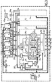
- FIG. 3 shows a diagram of an embodiment of a multiplexing device according to the invention.
- It is composed of a plurality of service circuits C1, C2, ..., C M each provided with an output S1, S2, ..., S M respectively connected to a common data line 200 and a plurality of network circuits R0, R1, R2 and R3, each provided with an input E0, E1, E2 and E3 also connected to this common line 200.
- each of the service circuits C1, C2, ..., C M the terminals 1801 to 1805 for the circuit C1 and the terminals 1806 to 180 N (not shown in FIG. 3 ) for other circuits.
- these circuits C1, C2, ..., C M are each assigned to a given service.
- circuit C1 is assigned to video links such as videoconferencing, circuit C2 to telephone links and circuit C M to extensions of local networks.
- Each circuit C1, C2, ..., C M comprises at least one queue member formed from a memory of the FIFO type (first input data, first output data). This is in practice achieved by means of a random access memory provided with independent read and write circuits.
- We identified by 205 Kohls to 205 P the different queue members contained in the circuit C1.
- These organs make it possible to store different information cells before they pass through the network 100.
- two wires 2061 to 206 P have been assigned on the one hand and 2071 to 207 P , on the other hand, for transmitting respectively a read command signal and an empty memory signal or, in other words, a signal to indicate whether or not the memory contains at least one cell.
- a switching device 250 makes it possible to switch the various access terminals to the queue members 2051 to 205 P.
- This switching member 250 can be coupled to a cell trainer 260 in case these are not formed at the level of the user. This need not be described in more detail since the invention is not concerned with this.
- the commutations carried out by the member 250 are defined by a table 262. This table is registered by means of a management member 270, which can be constituted by an individual computer like PC, to make a correspondence between one of the terminals of access 1801 to 1805 on which a user is connected and one of the queue members 2051 to 205 P.
- a table formed by a memory 275 makes it possible to manage, inside the service circuits, the access of the various queue members to line 200.
- This table also registered from the management member 270, allows to assign a queue member to a destination code being the concatenation of a VPI ("Virtual Path Identifier") and an identifier of the network access point.
- the VPI consists of 8 binary elements and since the number of network accesses is 4 in the example described here, a given destination is therefore represented by a code of 10 binary elements.
- This table is addressed by different destination codes coming from a first service line 280 common to all the service circuits C2, ..., C M. This table provides, in correspondence, the code validating or not a queue organ 205 organe to 205 P.
- a register 288 stores this validation code.
- An OR gate 290 supplies a signal DA1 which, active, signals that at least one queue member of the circuit C1 concerned by the access code contains at least one cell. This is determined by a set of doors ET 2951 to 295 P with two inputs; a first receives the allocation signal from register 288 and the second the signal transmitted by the wires 2071 to 207 P. The inputs of OR gate 290 receive the output signals from gates 2951 to 295 p .
- a decoding circuit 310 provides an active signal when a code corresponding to the identification code of the service circuit is transmitted by a second service line 315.
- the signal decoding from circuit 310 allows the selection of one of the queue members, if there is one concerned by this operation, via a validation circuit 316 which allows the codes contained therein to pass in the register 288 at each edge of a signal H supplied by a clock 317 and therefore activates the reading of the queue member concerned so that a cell is transmitted on the line 200.
- FIG. 4 shows in more detail the structure of the network circuit R0, it being understood that the other circuits R1, R2 and R3 can have the same structure.
- the circuit R0 includes an output circuit 400 which connects the common line 200 to the connection terminal 170.
- It also includes an allocation unit 410 for supplying destination codes at well-defined times.
- the member 410 is provided with an allocation table constituted by a random access memory 412 containing destination codes distributed in a manner which will be explained below and by a table reading member provided for picking up said codes. destination.
- the read member is constituted by an addressing counter 414 of said memory. This counter counts H1 pulses at a fixed rate so that the memory is read cyclically.
- This circuit R0 also includes an arbitration circuit 450.
- This circuit is formed by a processing circuit 455 whose outputs 465 provide the identification code of the service circuit to which access to line 200 has been granted.
- status memory 470 which contains previous states and in particular the identification code of the last service circuit which obtained access for one of the 256 destinations accessible from this network access, the VPI field having 8 binary elements wide.
- the entrees of the processing circuit 455 are constituted, on the one hand, by the signals DA1, DA2, ..., DA M passing through a buffer register 472 and on the other hand by the destination code transmitted on the line 280.
- the information multiplexing device further comprises an allocation member for allocating cell sampling times on said data line 200, to each of the output circuits as a function of the bit rate to be flowed by said output circuits.
- This member is formed from an allocation table in the form of a memory 500 which is addressed by a code of time interval numbers TS transmitted by a line 510 common to all the network circuits R0 , R1, R2 and R3. These time interval codes are produced by a counter 520 (fig. 3) counting the pulses of the signal H.
- the memory 500 is organized in words of a single binary element and has a number of locations equal to the counting capacity of the counter 520. In the context of this example: 64. In the locations of this memory 500, there are allocation indications. Thus, we put a logical "1" to signify that the network circuit is concerned by this time interval code and a "0" to signify that it is not concerned.
- This memory 500 is pre-programmed by means of the management unit 270 in a manner explained below.
- bit rates to be transmitted by the network circuits are low, their number can be multiplied without saturating the transmission capacity of line 200.
- the information multiplexing device described comprises pipeline registers which authorize operation in the pipeline. These different registers are clocked at the rate of the clock signal H.
- pipeline registers 515 and 516 are inserted in the lines of service 280 and 315.
- the other circuits C2 to C M are also obviously equipped with the same registers.
- a first pipeline register 550 interconnects the common data line 200 with the output circuit 400; this register is loaded at the rate of an H5 signal.
- a second register 552 and a third register 553 loaded at the rate of a signal H3 provide the different information to be processed by the arbitration circuit 450.
- register 552 receives the different signals DA1 to DA M and on the other hand the register 553 receives the code transmitted by the service line 280.
- the information produced by this arbitration circuit 450 is received by a fourth register 554 at the rate of a signal H4.
- a fifth register 556 interconnects the output of the allocation unit 410 with the service line 280.
- the signals H2, H3, H4 and H5 are deduced from the signal H1 by successive time offsets each equal to a period of the signal H.
- the signal H1 is derived from the signal H by an AND gate 580 with two inputs, one of which therefore receives the signal H and the other the value of the binary element contained in the memory 500 previously validated. This validation is carried out at the rate of the signal H by means of a flip-flop 582.
- the operation of the information multiplexing device of the invention is as follows.
- This management body 270 is the interface between a management manager who handles this body and the users, on the one hand, and a network manager, on the other hand.
- the manager determines the connections to be made between the various access terminals and the queue members.
- the device manager communicates with the network manager to reserve access with a certain speed.
- the latter provides following this request a destination code representing in a shortened form, as has been said, the destination desired by the recipient. It is from this member that the various table memories 262, 275, 412, 470 and 500 are loaded according to the traffic to be satisfied.
- the cells can be sent over each access link to the network 100 at a maximum rate of 149.76.106 eb / s (binary elements per second).
- the TS time interval codes vary from 0 to 63 and therefore the counter 520 is a modulo 64 counter.
- the network circuits are all called to transmit at this maximum rate, a maximum of 16 TS time codes are allocated among the 64 at each of the network circuits.
- the allocated TS time codes must be separated by at least 3 TS time codes. The period of the signal H is therefore 707.5 ns.
- FIG. 5 shows an example of allocation of these time intervals TS.
- the circuit R0 is assigned to the maximum bit rate, 16 TS codes are allocated to it either: the codes “0", “4", “8", “12", ...
- the circuit R1 is assigned to a bit rate twice as low .
- TS codes "1", “9”, ... are allocated to it.
- the circuit R2 is also assigned to this maximum speed the codes “2", “6", “10", “14”, ..., "62” are allocated to it.
- the circuit R3 is assigned to a slow rate and a single time code TS is allocated to it, ie "4".
- This allocation member 410 defines access times to common line 200 to the queue members contained in the various circuits C1, C2, ..., C M so that cells are emitted on the connection terminal 170 via the common line 200 and the output circuit 400.
- the memory 412 contains destination codes distributed in a manner explained below and the read counter 414 is provided to address this memory at the rate of the signal H1 so that the memory is read continuously in a cyclic manner. This fixes the rate of appearance of said destination codes.
- This memory 412 is also programmed from the management terminal 270.
- a manager takes into account the speed requests for the different destinations and formulates a request to obtain the necessary resources of the network for the envisaged traffic. This request is transferred to the network manager who provides the destination code consisting of a V.P.I. and a code identifying the network access circuit. The manager then writes this destination code into the memory 412 according to the following considerations.
- the frequency of the clock pulses fixes the maximum bit rate that can be transmitted. Either by taking a practical example 149.76.106 eb / s (binary elements per second), so the period for the H1 pulses cannot be less than 2.83 ⁇ s. Thus, if the traffic required for a destination is this maximum speed, all the memory locations will be affected by this service.
- the size of this memory is partly defined by the minimum flow rate d min to be guaranteed, for example: 4.5 103 eb / s.
- the memory size is then 32,768 locations. This size is also defined by the granularity of the bit rates to be transmitted, that is to say the set of different bit rates which can be transmitted. The greater the number of possible debits, the larger the size of the table.
- the memory 470 contains as many memory locations as there are possible VPI codes, namely: 256.
- the arbitration mechanism chosen is that of rotating priority, for each destination, described in "DISTRIBUTED-PROCESSOR COMMUNICATION ARCHITECTURE" by Kenneth J. Thurber, and Gerald M. Masson, published in Lexington Books, Heatch., Chapter 5, pages 140 and 141. Given this mechanism, memory 470 does not require any initialization.
- the priority is determined in several phases of calculations determined by a clock signal H16 which has a frequency sixteen times higher than that of the signals H.
- the arbitration context, for a given destination, is stored in memory 470, at an address deduced from the V.P.I. number. corresponding to this destination.
- a system comprising such a device can be formed from a network of the type shown in FIG. 1. This system then allows the exchange of information between nodes of this network via a device according to the invention.
Landscapes
- Engineering & Computer Science (AREA)
- Computer Networks & Wireless Communication (AREA)
- Computer Hardware Design (AREA)
- Signal Processing (AREA)
- Data Exchanges In Wide-Area Networks (AREA)
Applications Claiming Priority (2)
| Application Number | Priority Date | Filing Date | Title |
|---|---|---|---|
| FR9303776 | 1993-03-31 | ||
| FR9303776 | 1993-03-31 |
Publications (1)
| Publication Number | Publication Date |
|---|---|
| EP0618748A1 true EP0618748A1 (de) | 1994-10-05 |
Family
ID=9445585
Family Applications (1)
| Application Number | Title | Priority Date | Filing Date |
|---|---|---|---|
| EP94200810A Withdrawn EP0618748A1 (de) | 1993-03-31 | 1994-03-25 | Einrichtung und System zur Multiplexbildung der Information im ATM-Netz |
Country Status (3)
| Country | Link |
|---|---|
| US (1) | US5539738A (de) |
| EP (1) | EP0618748A1 (de) |
| JP (1) | JPH07183895A (de) |
Cited By (2)
| Publication number | Priority date | Publication date | Assignee | Title |
|---|---|---|---|---|
| EP0735793A1 (de) * | 1995-03-29 | 1996-10-02 | Philips Communication D'entreprise | Kommunikationssystem mit einem Netz und Multiplexgerät |
| EP0771130A1 (de) | 1995-10-25 | 1997-05-02 | Philips Communication D'entreprise | Multiplex- und Zuweisungsanlage für ein ATM-Netzwerk |
Families Citing this family (3)
| Publication number | Priority date | Publication date | Assignee | Title |
|---|---|---|---|---|
| JP3437071B2 (ja) * | 1997-10-28 | 2003-08-18 | 富士通株式会社 | Atmセル多重装置 |
| JP3679249B2 (ja) * | 1998-07-31 | 2005-08-03 | 富士通株式会社 | Atmセル多重装置 |
| FR2823037B1 (fr) | 2001-03-27 | 2003-06-20 | Thomson Csf | Procede d'optimisation de la gestion de la bande passante d'un canal de transmission numerique |
Citations (3)
| Publication number | Priority date | Publication date | Assignee | Title |
|---|---|---|---|---|
| EP0138717A2 (de) * | 1983-10-14 | 1985-04-24 | Denis Chomel | Asynchrones digitales Zeitmultiplexsystem mit verteiltem Bus |
| EP0351014A2 (de) * | 1988-07-14 | 1990-01-17 | Philips Patentverwaltung GmbH | Koppelfeld für ein Vermittlungssystem |
| FR2670972A1 (fr) * | 1990-12-20 | 1992-06-26 | Lmt Radio Professionelle | Commutateur de transit d'un reseau asynchrone, notamment un reseau atm. |
Family Cites Families (4)
| Publication number | Priority date | Publication date | Assignee | Title |
|---|---|---|---|---|
| US4597075A (en) * | 1981-08-21 | 1986-06-24 | Italtel-Societa Italiana Telecomunicazioni S.P.A. | Modular switching network for telecommunication system |
| FR2635243B1 (fr) * | 1988-08-05 | 1994-01-14 | Lmt Radio Professionnelle | Commutateur de paquets pour un transfert de donnees en mode asynchrone dans un reseau de transmission numerique |
| US5072442A (en) * | 1990-02-28 | 1991-12-10 | Harris Corporation | Multiple clock rate teleconferencing network |
| US5251209A (en) * | 1991-03-28 | 1993-10-05 | Sprint International Communications Corp. | Prioritizing attributes in integrated services networks |
-
1994
- 1994-03-25 EP EP94200810A patent/EP0618748A1/de not_active Withdrawn
- 1994-03-30 US US08/221,149 patent/US5539738A/en not_active Expired - Fee Related
- 1994-03-31 JP JP6293294A patent/JPH07183895A/ja active Pending
Patent Citations (3)
| Publication number | Priority date | Publication date | Assignee | Title |
|---|---|---|---|---|
| EP0138717A2 (de) * | 1983-10-14 | 1985-04-24 | Denis Chomel | Asynchrones digitales Zeitmultiplexsystem mit verteiltem Bus |
| EP0351014A2 (de) * | 1988-07-14 | 1990-01-17 | Philips Patentverwaltung GmbH | Koppelfeld für ein Vermittlungssystem |
| FR2670972A1 (fr) * | 1990-12-20 | 1992-06-26 | Lmt Radio Professionelle | Commutateur de transit d'un reseau asynchrone, notamment un reseau atm. |
Non-Patent Citations (1)
| Title |
|---|
| B. VOETEN ET AL, INT. SWITCHING SYMPOSIUM90, vol. 6, May 1990 (1990-05-01), SWEDEN, pages 25 - 28, XP000130957 * |
Cited By (3)
| Publication number | Priority date | Publication date | Assignee | Title |
|---|---|---|---|---|
| EP0735793A1 (de) * | 1995-03-29 | 1996-10-02 | Philips Communication D'entreprise | Kommunikationssystem mit einem Netz und Multiplexgerät |
| FR2732530A1 (fr) * | 1995-03-29 | 1996-10-04 | Trt Telecom Radio Electr | Systeme de communication comportant un reseau et dispositif de multiplexage convenant a un tel systeme |
| EP0771130A1 (de) | 1995-10-25 | 1997-05-02 | Philips Communication D'entreprise | Multiplex- und Zuweisungsanlage für ein ATM-Netzwerk |
Also Published As
| Publication number | Publication date |
|---|---|
| US5539738A (en) | 1996-07-23 |
| JPH07183895A (ja) | 1995-07-21 |
Similar Documents
| Publication | Publication Date | Title |
|---|---|---|
| EP0618749A1 (de) | Einrichtung und System zur Multiplexbildung der Information im ATM-Netz | |
| EP0293315B1 (de) | System und Verfahren zur Paketflusssteuerung | |
| CA2050405C (fr) | Systeme de memorisation temporaire d'information comprenant une memoire tampon enregistrant des donnees structurees en blocs de donnees de longueur fixe ou variable | |
| EP1507374B1 (de) | Verfahren und Vorrichtung zur Prioritätsverwaltung während der Übertragung einer Nachricht. | |
| EP0126196B1 (de) | Asynchrones Zeitmultiplexkoppelfeld zu Punkt-zu-Punkt-, Mehrpunkt- und Rundsendeverbindungen | |
| FR2694828A1 (fr) | Bus d'ordinateur à transfert de paquets. | |
| FR2617304A1 (fr) | Sequenceur d'entrees/sorties programmable pour processeur d'entree/sortie | |
| EP0601653A1 (de) | System zur Übertragung von Information mit unterschiedlichen Bitraten und Sendestation für ein solches System | |
| FR2616025A1 (fr) | Methode et systeme de controle de flux de paquets | |
| FR2701180A1 (fr) | Dispositif de cellulisation et dispositif de décellulisation de voies numériques synchromes, centre de commutation de voies numériques synchrones, et centre de commutation de voies numériques asynchrones. | |
| EP0383660B1 (de) | Ratenreservierung in einem asynchronen Paketnetzwerk | |
| EP0920157A1 (de) | Verwaltungseinrichtung eines gemeinsamen Pufferspeichers | |
| FR2736779A1 (fr) | Appareil de commutation de donnees ,par exemple dans des reseaux a mode de transport asynchrone | |
| FR2549673A1 (fr) | Commutateur elementaire pour autocommutateur utilisant une technique de multiplexage asynchrone | |
| FR2824434A1 (fr) | Procede de diffusion d'un paquet de donnees au sein d'un reseau commute, base sur un calcul optimise de l'arbre de recouvrement | |
| EP0020255B1 (de) | Vermittlungsebene eines Operators für Datenpaketvermittlungsnetz | |
| EP0689371A1 (de) | Kommunikationssystem mit einem Netz und einer Multiplexeinheit | |
| FR2653285A1 (fr) | Dispositif d'evaluation du debit de circuits virtuels empruntant une voie de transmission a multiplexage temporel asynchrone. | |
| FR2649269A1 (fr) | Systemes complementaires de communication en mode sans-connexion pour reseau temporel asynchrone | |
| EP0771130B1 (de) | Multiplex- und Zuweisungsgerät für ein ATM-Netzwerk | |
| EP0899917B1 (de) | Vorrichtung und Verfahren zur ATM-Gruppenvermittlung mit Zugehörigen Endfunktionen im Eingang und Ausgang | |
| EP0114433B1 (de) | Fernsprechvermittlungssystem | |
| EP0632669B1 (de) | Kommunikationssystem mit ATM-Netz und -Demultiplexer | |
| EP0652662A1 (de) | Anordnung für Warteschlangen zur Verwendung in der Eingangsstufe eines nicht blockierenden Raumschaltes | |
| FR2758427A1 (fr) | Element de commutation, notamment de cellules atm, mettant en oeuvre des priorites probabilistes attachees aux cellules |
Legal Events
| Date | Code | Title | Description |
|---|---|---|---|
| PUAI | Public reference made under article 153(3) epc to a published international application that has entered the european phase |
Free format text: ORIGINAL CODE: 0009012 |
|
| AK | Designated contracting states |
Kind code of ref document: A1 Designated state(s): DE FR GB |
|
| 17P | Request for examination filed |
Effective date: 19950405 |
|
| RAP1 | Party data changed (applicant data changed or rights of an application transferred) |
Owner name: PHILIPS ELECTRONICS N.V. Owner name: PHILIPS COMMUNICATION D'ENTREPRISE |
|
| RAP1 | Party data changed (applicant data changed or rights of an application transferred) |
Owner name: COMPAGNIE DES SIGNAUX Owner name: PCE |
|
| RAP1 | Party data changed (applicant data changed or rights of an application transferred) |
Owner name: CS COMMUNICATION & SYSTEMES Owner name: PCE |
|
| STAA | Information on the status of an ep patent application or granted ep patent |
Free format text: STATUS: THE APPLICATION HAS BEEN WITHDRAWN |
|
| 18W | Application withdrawn |
Withdrawal date: 20020323 |