EP0619559A2 - Integrierte analog-digitale Grenzschnittstelle - Google Patents
Integrierte analog-digitale Grenzschnittstelle Download PDFInfo
- Publication number
- EP0619559A2 EP0619559A2 EP94302338A EP94302338A EP0619559A2 EP 0619559 A2 EP0619559 A2 EP 0619559A2 EP 94302338 A EP94302338 A EP 94302338A EP 94302338 A EP94302338 A EP 94302338A EP 0619559 A2 EP0619559 A2 EP 0619559A2
- Authority
- EP
- European Patent Office
- Prior art keywords
- converter
- analog
- circuit
- boundary interface
- programmable
- Prior art date
- Legal status (The legal status is an assumption and is not a legal conclusion. Google has not performed a legal analysis and makes no representation as to the accuracy of the status listed.)
- Withdrawn
Links
Images


Classifications
-
- G—PHYSICS
- G06—COMPUTING OR CALCULATING; COUNTING
- G06J—HYBRID COMPUTING ARRANGEMENTS
- G06J1/00—Hybrid computing arrangements
Definitions
- This invention relates to an integrated analog-digital boundary interface for time multiplexed communication systems.
- time multiplexed digital cellular systems In time multiplexed digital cellular systems (TDMA, Time Division Multiple Access), such as GSM and digital AMPS, transmitting and receiving alternate in time slots.
- TDMA Time Division Multiple Access
- GSM Global System for Mobile Communications
- digital AMPS In digital transmitters one or more D/A converters are used and likewise in the receivers one or more A/D converters, are used.
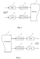
- Figure 1 is a block diagram of a prior art digital carrier frequency receiver.
- Figure 2 is a block diagram of a prior art digital carrier frequency transmitter.
- FIG. 3 is a block diagram of a prior art Analog Front End (AFE) circuit used in digital communication systems.
- AFE Analog Front End
- the diagram shown in figure 1 is a block diagram of a prior art digital carrier frequency receiver.
- An incoming carrier frequency signal is brought to A/D converters 3, 4 through filters 1, 2.
- the converted signal is brought to a digital receiver 5.
- FIG 2 is a block diagram of a prior art digital carrier frequency transmitter.
- a digital transmitter 6 transmits the signal to D/A converters 7, 8.
- the converted signal is brought to filters 9, 10, which output the carrier frequency signal.
- FIG 3 is a block diagram of a prior art digital communication system's Analog Front End (AFE) circuit.
- the filters 1, 2, 9, 10 and converters 3, 4, 7, 8 have been integrated on the common AFE integrated circuit (IC) 12.
- the digital receiver/transmitter unit is marked with reference numeral 11.
- Analog Front End (AFE) circuit 12 there are one or more A/D converters 3, 4 in a receiver branch and one or more D/A converters 7,8 in a transmitter branch. In the same circuit there are also typically receiver filters 1,2 and corresponding transmitter filters 9, 10 for the intermediate frequency carrier. As the circuit is commonly integrated with CMOS technology, all the functions can be laid out on the same integrated circuit 12. This takes up a lot of the chip area of the circuit 12. A complex circuit causes a lot of coupling interference and noise and makes the circuit itself sensitive to other interference sources.
- an integrated analog-digital boundary interface having a circuit for transmitting and receiving signals in burst mode during respective predetermined time slots comprising a converter programmable to function as an A/D converter during periods corresponding to the predetermined receiving time slots and as a D/A converter during periods corresponding to the predetermined transmitting time slots.
- An advantage of this invention is that by using the respective outputting and receiving periods a single programmable converter can be utilised as an A/D converter during a first period and a D/A converter during a second period with a beneficial reduction in the number of components used in the circuit board.
- the reduction in complexity also alleviates the previously mentioned interference problems.
- the analog-digital boundary interface may further include a programmable filter. This further reduces the number of components with additional improvements in interference and space saving.
- FIG. 4 is a block diagram of an Analog Front End (AFE) circuit of a digital communication system according to an embodiment of the present invention.
- AFE Analog Front End
- Figure 5 is a block diagram of a Serial Approximation Register type A/D converter according to an embodiment of the present invention.
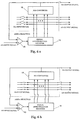
- Figure 6a is a block diagram of a programmable Serial Approximation Register type converter capable of functioning as an A/D converter.
- Figure 6b is a block diagram corresponding to that of Figure 6a with the converter functioning as a D/A converter.
- the diagram shown in figure 4 is a block diagram of an Analog Front End circuit of a communication system according to an embodiment of the present invention.
- the programmable filters 13, 14 and programmable converters 15, 16 are integrated to the same Analog Front End integrated circuit 17.
- the digital receiver/transmitter unit is marked with the reference numeral 11.
- the transmitting and receiving operations can be implemented using some of the same circuit elements of the integrated Analog Front End circuit 17 in both the receiving branch and the transmitting branch.
- a good quality D/A converter is an integral component of a Serial Approximation Register type A/D converter.
- the transmitter and the receiver operate in separate time slots (time multiplexed), so only one good quality programmable converter 15, 16 is needed in this circuit for each pair of conventional A/D and D/A converters.
- the diagram shown in figure 5 is a block diagram of a Serial Approximation Register (SAR) type A/D converter.
- the SAR-type A/D converter comprises a D/A converter 18, a serial approximation register 19 and an operational amplifier (comparator) 20.
- the diagram shown in figure 6 is a block diagram of a programmable, generic Serial Approximation Register type converter.
- the programmable SAR-type converter 15, 16 comprises a D/A converter 18, a serial approximation register 19 and an operational amplifier (comparator) 20.
- the generic converter 15, 16 is programmed as an A/D converter. There can be several converters 15, 16 operating in parallel. During transmitting periods the converter 15, 16 functions as a D/A converter. Generality causes an inevitable decrease in performance, but this can be compensated for in advance during the design phase.
- the programmable bi-directional converter 15, 16 also requires a larger area on the integrated circuit than a dedicated and optimized one-directional converter, but there is a significant total area saving in the system.
- connections can be designed to be programmable, as shown previously, and their use can also be changed to comply with the requirements of a particular time slot.
- a considerable amount of circuit board or integrated circuit area can thereby be saved along with a reduction in the complexity and interference sensitivity of the circuit.
- the branch filters 13, 14 are usually integrated by CMOS technology using Switched Capacitor (SC) technology.
- SC Switched Capacitor
- a programmable, generic converter 15, 16 is connected to a programmable, generic filter 13, 14 by a switch network that is programmable to take a receiving or transmitting state.
- the time needed for the circuit to change from the receiving state to the transmitting state, or vice versa, is a fraction of the time available for this operation in, for example, GSM or digital AMPS type cellular systems.
- the invention is not limited to carrier frequency or intermediate frequency applications, but is applicable to any time division communication system.
- the AFE circuit 17 can also provide other independent functions which this invention does not affect.
- the communication system's time multiplexing is carried to implementation level by taking full advantage of the time slots allocated to the transmit and receive periods.
- the surface area of the integrated circuit and cost is reduced by implementing both the carrier frequency filtration or the intermediate frequency filtration and the bi-directional conversions (A/D and D/A) with programmable, generic circuit element or elements.
- programmable elements By utilising programmable elements in this manner, there is also less interference or noise than in prior art circuits, since there are less functioning circuit elements in use.
- the AFE circuit 17 according to an embodiment of this invention there are no separate branches for receiving and transmitting as these functions are accomplished by the common programmable circuits.
- the invention can be applied to any time division communication system, such as, for example, GSM or digital AMPS digital cellular applications.
- the invention is a cost-effective manner for the implementation of the above mentioned TDMA type systems.
Landscapes
- Engineering & Computer Science (AREA)
- Physics & Mathematics (AREA)
- Theoretical Computer Science (AREA)
- Computer Hardware Design (AREA)
- Mathematical Physics (AREA)
- Automation & Control Theory (AREA)
- Evolutionary Computation (AREA)
- Fuzzy Systems (AREA)
- General Physics & Mathematics (AREA)
- Software Systems (AREA)
- Analogue/Digital Conversion (AREA)
Applications Claiming Priority (2)
| Application Number | Priority Date | Filing Date | Title |
|---|---|---|---|
| US4272293A | 1993-04-05 | 1993-04-05 | |
| US42722 | 1993-04-05 |
Publications (2)
| Publication Number | Publication Date |
|---|---|
| EP0619559A2 true EP0619559A2 (de) | 1994-10-12 |
| EP0619559A3 EP0619559A3 (de) | 1995-10-25 |
Family
ID=21923412
Family Applications (1)
| Application Number | Title | Priority Date | Filing Date |
|---|---|---|---|
| EP94302338A Withdrawn EP0619559A3 (de) | 1993-04-05 | 1994-03-31 | Integrierte analog-digitale Grenzschnittstelle. |
Country Status (1)
| Country | Link |
|---|---|
| EP (1) | EP0619559A3 (de) |
Family Cites Families (5)
| Publication number | Priority date | Publication date | Assignee | Title |
|---|---|---|---|---|
| US4160243A (en) * | 1976-09-28 | 1979-07-03 | Fujitsu Limited | Asynchronous reversible analog to digital converter |
| DE2643687C2 (de) * | 1976-09-28 | 1983-09-29 | Siemens AG, 1000 Berlin und 8000 München | Schaltungsanordnung zur Übertragung von Digital-Signalen zwischen Teilnehmerstellen eines Zeitmultiplex-Fernmeldenetzes, insbesondere PCM-Zeitmultiplex- Fernmeldenetzes |
| US4348768A (en) * | 1977-09-06 | 1982-09-07 | International Telephone And Telegraph Corporation | PCM Codec using common D/A converter for encoding and decoding |
| EP0313706B1 (de) * | 1987-10-30 | 1992-04-29 | International Business Machines Corporation | Analog-Digital/Digital-Analogwandlersystem und Gerät zur Echoannullierung unter Verwendung eines solchen Systems |
| US5021783A (en) * | 1990-09-27 | 1991-06-04 | Advanced Micro Devices, Inc. | Method for operating an apparatus for facilitating communications |
-
1994
- 1994-03-31 EP EP94302338A patent/EP0619559A3/de not_active Withdrawn
Also Published As
| Publication number | Publication date |
|---|---|
| EP0619559A3 (de) | 1995-10-25 |
Similar Documents
| Publication | Publication Date | Title |
|---|---|---|
| US6078622A (en) | Distributed digital radio system | |
| EP0486181B1 (de) | Mobiles Funktelefon | |
| US4435821A (en) | Receiver in a frequency hopping communication system | |
| KR20010089742A (ko) | 멀티 스탠다드 통신 단말기용 회로 | |
| JP2007504717A (ja) | 送受信機において信号をフィルタリングするためのシステムおよび方法 | |
| EP0829970A2 (de) | Zweimodusfunkgerät für TDMA und FDD | |
| EP0752761A3 (de) | FDMA-Funkgerätschaltung mit variablem zweiten Lokaloszillator | |
| WO2000036798A3 (en) | Network data filtering | |
| EP0680156B1 (de) | Funkgerät und entsprechendes Übertragungsverfahren | |
| WO1998028839A1 (en) | Dpsk demodulator | |
| US6922554B2 (en) | Method for implementing a transceiver and a transceiver | |
| US20030147459A1 (en) | Interface concept for the exchange of digital signals between an rf ic and a baseband ic | |
| EP1260027A2 (de) | Korrekturschaltung für gleichspannungsoffset mit gleichspannungsregelungsschleife und gleichspannungsblockierungsschaltung | |
| EP0529767A1 (de) | Digitales Funkgerät | |
| EP0619559A2 (de) | Integrierte analog-digitale Grenzschnittstelle | |
| US6807237B1 (en) | Radio apparatus and transmission/reception method | |
| EP1762943A8 (de) | Chip-zu-chip Kommunikationssystem | |
| EP0449612B1 (de) | Analoge Eingangsmehrzweckschaltung | |
| KR100432987B1 (ko) | 통신 단말기용 수신 회로 및 수신 회로에서의 신호 처리방법 | |
| US6831582B2 (en) | Method and circuit configuration for mixing a digital signal with an analogue signal | |
| US20050276351A1 (en) | Receiving arrangement of a cordless communication system | |
| JPH0974369A (ja) | デジタル双方向通信高周波装置 | |
| CN212909516U (zh) | 一种用于信号处理的新型数字板卡 | |
| US7133464B2 (en) | Transmission apparatus | |
| JP2708485B2 (ja) | 無線電話用信号処理回路 |
Legal Events
| Date | Code | Title | Description |
|---|---|---|---|
| PUAI | Public reference made under article 153(3) epc to a published international application that has entered the european phase |
Free format text: ORIGINAL CODE: 0009012 |
|
| AK | Designated contracting states |
Kind code of ref document: A2 Designated state(s): DE FR GB |
|
| RIN1 | Information on inventor provided before grant (corrected) |
Inventor name: MYLLYMAKI, KIMMO |
|
| PUAL | Search report despatched |
Free format text: ORIGINAL CODE: 0009013 |
|
| AK | Designated contracting states |
Kind code of ref document: A3 Designated state(s): DE FR GB |
|
| 17P | Request for examination filed |
Effective date: 19960425 |
|
| 17Q | First examination report despatched |
Effective date: 19990922 |
|
| STAA | Information on the status of an ep patent application or granted ep patent |
Free format text: STATUS: THE APPLICATION IS DEEMED TO BE WITHDRAWN |
|
| 18D | Application deemed to be withdrawn |
Effective date: 20000203 |