EP0619599A1 - Monokristallines Dünnschichtsubstrat - Google Patents
Monokristallines Dünnschichtsubstrat Download PDFInfo
- Publication number
- EP0619599A1 EP0619599A1 EP94106060A EP94106060A EP0619599A1 EP 0619599 A1 EP0619599 A1 EP 0619599A1 EP 94106060 A EP94106060 A EP 94106060A EP 94106060 A EP94106060 A EP 94106060A EP 0619599 A1 EP0619599 A1 EP 0619599A1
- Authority
- EP
- European Patent Office
- Prior art keywords
- single crystal
- thin film
- silicon carbide
- diamond
- silicon
- Prior art date
- Legal status (The legal status is an assumption and is not a legal conclusion. Google has not performed a legal analysis and makes no representation as to the accuracy of the status listed.)
- Granted
Links
Images
Classifications
-
- H—ELECTRICITY
- H10—SEMICONDUCTOR DEVICES; ELECTRIC SOLID-STATE DEVICES NOT OTHERWISE PROVIDED FOR
- H10P—GENERIC PROCESSES OR APPARATUS FOR THE MANUFACTURE OR TREATMENT OF DEVICES COVERED BY CLASS H10
- H10P14/00—Formation of materials, e.g. in the shape of layers or pillars
- H10P14/20—Formation of materials, e.g. in the shape of layers or pillars of semiconductor materials
- H10P14/29—Formation of materials, e.g. in the shape of layers or pillars of semiconductor materials characterised by the substrates
- H10P14/2901—Materials
- H10P14/2902—Materials being Group IVA materials
- H10P14/2903—Carbon, e.g. diamond-like carbon
-
- H—ELECTRICITY
- H10—SEMICONDUCTOR DEVICES; ELECTRIC SOLID-STATE DEVICES NOT OTHERWISE PROVIDED FOR
- H10P—GENERIC PROCESSES OR APPARATUS FOR THE MANUFACTURE OR TREATMENT OF DEVICES COVERED BY CLASS H10
- H10P14/00—Formation of materials, e.g. in the shape of layers or pillars
- H10P14/20—Formation of materials, e.g. in the shape of layers or pillars of semiconductor materials
- H10P14/24—Formation of materials, e.g. in the shape of layers or pillars of semiconductor materials using chemical vapour deposition [CVD]
-
- H—ELECTRICITY
- H10—SEMICONDUCTOR DEVICES; ELECTRIC SOLID-STATE DEVICES NOT OTHERWISE PROVIDED FOR
- H10P—GENERIC PROCESSES OR APPARATUS FOR THE MANUFACTURE OR TREATMENT OF DEVICES COVERED BY CLASS H10
- H10P14/00—Formation of materials, e.g. in the shape of layers or pillars
- H10P14/20—Formation of materials, e.g. in the shape of layers or pillars of semiconductor materials
- H10P14/32—Formation of materials, e.g. in the shape of layers or pillars of semiconductor materials characterised by intermediate layers between substrates and deposited layers
- H10P14/3202—Materials thereof
- H10P14/3204—Materials thereof being Group IVA semiconducting materials
- H10P14/3206—Carbon, e.g. diamond-like carbon
-
- H—ELECTRICITY
- H10—SEMICONDUCTOR DEVICES; ELECTRIC SOLID-STATE DEVICES NOT OTHERWISE PROVIDED FOR
- H10P—GENERIC PROCESSES OR APPARATUS FOR THE MANUFACTURE OR TREATMENT OF DEVICES COVERED BY CLASS H10
- H10P14/00—Formation of materials, e.g. in the shape of layers or pillars
- H10P14/20—Formation of materials, e.g. in the shape of layers or pillars of semiconductor materials
- H10P14/34—Deposited materials, e.g. layers
- H10P14/3402—Deposited materials, e.g. layers characterised by the chemical composition
- H10P14/3404—Deposited materials, e.g. layers characterised by the chemical composition being Group IVA materials
- H10P14/3408—Silicon carbide
-
- H—ELECTRICITY
- H10—SEMICONDUCTOR DEVICES; ELECTRIC SOLID-STATE DEVICES NOT OTHERWISE PROVIDED FOR
- H10P—GENERIC PROCESSES OR APPARATUS FOR THE MANUFACTURE OR TREATMENT OF DEVICES COVERED BY CLASS H10
- H10P14/00—Formation of materials, e.g. in the shape of layers or pillars
- H10P14/20—Formation of materials, e.g. in the shape of layers or pillars of semiconductor materials
- H10P14/34—Deposited materials, e.g. layers
- H10P14/3402—Deposited materials, e.g. layers characterised by the chemical composition
- H10P14/3404—Deposited materials, e.g. layers characterised by the chemical composition being Group IVA materials
- H10P14/3411—Silicon, silicon germanium or germanium
-
- H—ELECTRICITY
- H10—SEMICONDUCTOR DEVICES; ELECTRIC SOLID-STATE DEVICES NOT OTHERWISE PROVIDED FOR
- H10P—GENERIC PROCESSES OR APPARATUS FOR THE MANUFACTURE OR TREATMENT OF DEVICES COVERED BY CLASS H10
- H10P14/00—Formation of materials, e.g. in the shape of layers or pillars
- H10P14/20—Formation of materials, e.g. in the shape of layers or pillars of semiconductor materials
- H10P14/34—Deposited materials, e.g. layers
- H10P14/3438—Doping during depositing
- H10P14/3441—Conductivity type
- H10P14/3442—N-type
-
- H—ELECTRICITY
- H10—SEMICONDUCTOR DEVICES; ELECTRIC SOLID-STATE DEVICES NOT OTHERWISE PROVIDED FOR
- H10P—GENERIC PROCESSES OR APPARATUS FOR THE MANUFACTURE OR TREATMENT OF DEVICES COVERED BY CLASS H10
- H10P14/00—Formation of materials, e.g. in the shape of layers or pillars
- H10P14/20—Formation of materials, e.g. in the shape of layers or pillars of semiconductor materials
- H10P14/34—Deposited materials, e.g. layers
- H10P14/3438—Doping during depositing
- H10P14/3441—Conductivity type
- H10P14/3444—P-type
-
- Y—GENERAL TAGGING OF NEW TECHNOLOGICAL DEVELOPMENTS; GENERAL TAGGING OF CROSS-SECTIONAL TECHNOLOGIES SPANNING OVER SEVERAL SECTIONS OF THE IPC; TECHNICAL SUBJECTS COVERED BY FORMER USPC CROSS-REFERENCE ART COLLECTIONS [XRACs] AND DIGESTS
- Y10—TECHNICAL SUBJECTS COVERED BY FORMER USPC
- Y10S—TECHNICAL SUBJECTS COVERED BY FORMER USPC CROSS-REFERENCE ART COLLECTIONS [XRACs] AND DIGESTS
- Y10S438/00—Semiconductor device manufacturing: process
- Y10S438/931—Silicon carbide semiconductor
Definitions
- the present invention relates to a thin film single crystal substrate which is useful in the production of a semiconductor. More particularly, it relates to a thin film single crystal substrate comprising a single crystal diamond base and at least one film of a single crystal material formed thereon.
- silicon carbide has been studied as a material for a heat and environment resistant element or a light-emitting element since it has several crystal structures and band gap of 2.2 to 3.3 eV depending on the crystal structure, its heat conductivity is as large as 4.9 W/cm.K, its maximum electron mobility is confirmed to be 1,000 cm2/V.sec., and it is possible to control p-type and n-type valence electrons.
- silicon carbide The crystal structures of silicon carbide are roughly classified into an ⁇ -type and a ⁇ -type. Since silicon carbide of the ⁇ -type hexagonal system (6H) has a large band gap of about 2.9 eV, it is believed that it can be used as a material for a blue light-emitting element. Silicon carbide of the ⁇ -type cubic system (3C) has a large electron mobility, it is investigated as a material for an environment resistant element.
- the single crystal of silicon carbide is formed by growing it on a silicon single crystal or sapphire in a gas or liquid phase (cf. Japanese Patent Kokai Publication Nos. 83588/1978 and 146299/1978).
- the silicon single crystal has various drawbacks. For example, since it has a band gap of 1.1 eV which is smaller than that of the silicon carbide single crystal, it has smaller resistivity at high temperature. It has a low melting point and a small thermal conductivity of 1.5 W/cm.K). Because of these characteristics of silicon carbide, when the silicon carbide single crystal is grown on the silicon single crystal, the advantages of the latter as the heat resistant semiconductive material are greatly impaired. Therefore, the silicon carbide single crystal grown on the silicon single crystal is used by removing the latter with an acid, but the remaining thin film of the silicon carbide has a thickness of several ten ⁇ m and is easily cracked or strained, which deteriorates its handling properties.
- sapphire is an insulating material up to high temperature and thermally stable, it has some drawbacks such as a small coefficient of thermal conductivity of 0.11 W/cm.K and a large coefficient of thermal expansion of 7.8 x 10 ⁇ 6/K.
- One object of the present invention is to provide a substrate having a large coefficient of thermal conductivity.
- Another object of the present invention is to provide a substrate having a small coefficient of thermal expansion.
- Further object of the present invention is to provide a substrate having good resistance against heat and/or environment.
- a thin film single crystal substrate which comprises a base substrate made of single crystal diamond and at least one thin film of a single crystal of a material selected from the group consisting of silicon carbide, silicon, boron nitride, gallium nitride, indium nitride, aluminum nitride, boron phosphide, cadmium selenide, germanium, gallium arsenide, gallium phosphide, indium phosphide, gallium antimonide, indium arsenide, indium antimonide, aluminum phosphide, aluminum arsenide, aluminum antimonide, cadmium telluride, mercury sulfide, zinc oxide, zinc sulfide, zinc selenide and zinc telluride, and optionally an intermediate layer between the base substrate and the thin film of single crystal.
- the diamond single crystal has a larger coefficient of thermal conductivity and a smaller relative dielectric constant than other materials as shown in Table 1.
- Table 1 Band gap (eV) Coefficient of thermal conductivity (W/cm.K) Relative dielectric constant Diamond 5.5 20 5.7 Silicon carbide 2.2-3.3 4.9 10 Silicon 1.1 1.5 12 Sapphire --- 0.11 10.5
- the base substrate may be made of natural or artificial diamond.
- an artificial single crystal diamond of several millimeter square having less impurities (particularly, nitrogen) is produced by the extra-high pressure method.
- the extra-high pressure method it is possible to produce a p-type semiconductive single crystal diamond, namely the IIb type, which is suitable for the production of a high power element.
- a p-type semiconductive single crystal diamond namely the IIb type
- an electrode is provided on the single crystal diamond.
- the single crystal diamond is a p-type semiconductive diamond which contains at least one of boron and aluminum as an impurity.
- the plane of the single crystal diamond of the base on which the single crystal thin film and/or the intermediate layer is grown may have any of orientations (100), (110), (111) and (211). Since the (111) plane orientation is difficult to abrase, the (100) and (110) orientations are preferred.
- the thickness of the diamond base is usually from 0.05 mm to 5 mm, preferably from 0.1 mm to 0.5 mm.
- the single crystal thin film formed on the single crystal diamond consists of at least one single crystal of a material selected from the group consisting of silicon carbide, silicon, boron nitride, gallium nitride, indium nitride, aluminum nitride, boron phosphide, cadmium selenide, germanium, gallium arsenide, gallium phosphide, indium phosphide, gallium antimonide, indium arsenide, indium antimonide, aluminum phosphide, aluminum arsenide, aluminum antimonide, cadmium telluride, mercury sulfide, zinc oxide, zinc sulfide, zinc selenide and zinc telluride.
- the single crystal may be a mixed crystal. Further, two or more thin films of the single crystal may be formed.
- the thickness of the thin film single crystal is usually from 100 to 100,000 ⁇ , preferably from 500 to 20,000 ⁇ .
- the single crystal thin layer preferably made of cubic system or hexagonal system silicon carbide single crystal. Two or more of such thin layers can be laminated.
- the single crystal thin layer preferably made of p-type silicon carbide single crystal which contains at least one impurity element selected from the group consisting of boron, aluminum, gallium and indium or n-type silicon carbide single crystal which contains at least one impurity element selected from the group consisting of nitrogen, phosphorus, arsenic, antimony and lithium. Two or more of the p-type single crystal thin films and/or the n-type single crystal thin films may be laminated.
- the thin film single crystal may be formed on the diamond base by any of conventional methods such as gas phase methods (e.g. the sublimation method, the thermal CVD method, the plasma CVD method, the reaction deposition method and the MBE method) and liquid phase methods.
- gas phase methods e.g. the sublimation method, the thermal CVD method, the plasma CVD method, the reaction deposition method and the MBE method
- liquid phase methods e.g. the sublimation method, the thermal CVD method, the plasma CVD method, the reaction deposition method and the MBE method
- the thin film single crystal substrate of the present invention may comprise an intermediate layer between the diamond base and the thin film of single crystal.
- the single crystal diamond has a lattice constant of 3.5667 ⁇
- the silicon single crystal has a lattice constant of 5.4301 ⁇ .
- the intermediate layer may be made of single crystal silicon carbide or single crystal diamond.
- the single crystal silicon carbide can be formed by the CVD (chemical vapor phase deposition) method, the modified CVD (MCVD) method, the MBE (molecular beam epitaxy) method.
- the single crystal diamond can be formed by the thermal CVD method, the plasma CVD method, the electron beam CVD method, the ion sputtering method, the optical CVD method and the like.
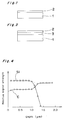
- the thin film single crystal substrate consists of the single crystal diamond base 1 and the single crystal thin layer 2 as shown in Fig. 1 or consists of the single crystal diamond base 1, the intermediate layer 3 and the single crystal thin film 2 as shown in Fig. 2.
- a thin film of silicon having a thickness of 5,000 ⁇ was formed by plasma CVD from a mixture of monosilane (SiH4) and hydrogen (molar ratio of 1:50) at 1,050°C under reduced pressure of 5 Torr.
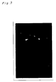
- the substrate After heating the produced substrate at 900°C under reduced pressure of 1 x 10 ⁇ 8 Torr, the substrate was observed by reflection electron beam diffraction to give a photograph of Fig. 3.
- the diffraction pattern had the Kikuchi Line, which indicated that the silicon thin film consisted of single crystal with good quality.
- a silicon carbide thin film having a thickness of 500 ⁇ m was formed by CVD from a mixture of monosilane, propane and hydrogen (a molar ratio of 1:4:95) at 1,350°C under reduced pressure of 400 Torr for 20 minutes.
- an n-type phosphorus-doped silicon film was grown by CVD from a mixture of monosilane, PH3 and hydrogen (a molar ratio of 105:1:107) at 1,050°C under reduced pressure of 100 Torr. for 30 minutes.
- the reflection electron beam diffraction pattern of the formed silicon film had the Kikuchi Line, which indicated that the silicon thin film consisted of single crystal.
- the n-type silicon film had a carrier density of 3 x 10¹⁷/cm3 and electron mobility of 900 cm2/V.sec.
- a piece of Ia type natural single crystal diamond (2 x 2 x 0.3 mm) with the (111) plane exposed was placed in a quartz reactor. After evacuating the reactor, monosilane, propane and hydrogen were supplied to the reactor at a flow ratio of 1:4:95 with keeping a temperature of the diamond single crystal at 1,300°C by an infrared heater for 30 minutes. A thin film of silicon carbide single crystal was formed on the (111) plane of the single crystal diamond.
- the silicon carbide crystal on the diamond was observed by reflective electron beam diffraction. Clear spots were observed, which confirmed the formation of single crystal thin film.
- the lattice constant a0 of silicon carbide single crystal was calculated to be 4.38 ⁇ , which substantially coincides with that of the cubic system (3C) silicon carbide (4.36 ⁇ ).
- a thin film of p-type semiconductive single crystal diamond having a thickness of 2.0 ⁇ m was formed by the conventional microwave plasma CVD method with microwave power of 300 W under reduced pressure of 55 Torr with flowing methane, diboran and hydrogen at a flow ratio of 103:1:105 in the quartz reactor.
- a silicon carbide single crystal film was formed by the same microwave plasma CVD method as above but using the microwave power of 500 W and reduced pressure of 200 Torr. with flowing monosilane, methane, hydrogen and argon at a flow ratio of 1:3:46:50 for one hour during which the substrate temperature was kept at 1,250°C.
- the reflective electron beam diffraction pattern of the silicon carbide single crystal film had spots and the Kikuchi Line, which indicated that the crystal was the cubic system (3C) silicon carbide single crystal.
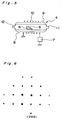
- a thin film single crystal was formed by using an apparatus shown in Fig. 5, which comprises a double-walled quartz tube 4, a supporting plate 6 made of graphite covered with silicon carbide, a 400 KHz high-frequency oscillator 7, an inlet 8 and an outlet 9 for cooling water, a (water cooled) work coil 10, and an inlet 11 and an outlet 2 for gasses.
- a piece 5 of single crystal of IIb type natural diamond (2 x 2 x 0.5 mm) was placed on the supporting plate 6.
- an AC current of 400 KHz and 2 KW was applied to the work coil 10 with supplying hydrogen gas in the tube to keep the pressure at 80 Torr.
- nitrogen, monosilane, propane and hydrogen were supplied at a flow ratio of 1:50:100:2,000 into the tube for 20 minutes under reduced pressure of 80 Torr to grow n-type silicon carbide single crystal.
- diboran, monosilane, propane and hydrogen were supplied at the flow ratio of 0.2:50:100:2,000 for 30 minutes under the same conditions to grow p-type silicon carbide single crystal.
- a piece of Ib type single crystal artificial diamond was placed in a graphite crucible together with hexagonal system silicon carbide powder and heated to 1,750°C under reduced pressure of 0.5 Torr while supplying argon gas to grow silicon carbide crystal on the surface of the diamond piece for 15 minutes by sublimation of silicon carbide.
Landscapes
- Crystals, And After-Treatments Of Crystals (AREA)
Applications Claiming Priority (7)
| Application Number | Priority Date | Filing Date | Title |
|---|---|---|---|
| JP5838387 | 1987-03-12 | ||
| JP58383/87 | 1987-03-12 | ||
| JP5838387A JPH0810670B2 (ja) | 1987-03-12 | 1987-03-12 | 薄膜単結晶シリコン基板 |
| JP62200460A JP2664056B2 (ja) | 1987-08-10 | 1987-08-10 | 薄膜単結晶基板 |
| JP20046087 | 1987-08-10 | ||
| JP200460/87 | 1987-08-10 | ||
| EP88103887A EP0282075B1 (de) | 1987-03-12 | 1988-03-11 | Monokristallines Dünnschichtsubstrat |
Related Parent Applications (3)
| Application Number | Title | Priority Date | Filing Date |
|---|---|---|---|
| EP88103887.1 Division | 1988-03-11 | ||
| EP88103887A Division-Into EP0282075B1 (de) | 1987-03-12 | 1988-03-11 | Monokristallines Dünnschichtsubstrat |
| EP88103887A Division EP0282075B1 (de) | 1987-03-12 | 1988-03-11 | Monokristallines Dünnschichtsubstrat |
Publications (2)
| Publication Number | Publication Date |
|---|---|
| EP0619599A1 true EP0619599A1 (de) | 1994-10-12 |
| EP0619599B1 EP0619599B1 (de) | 2001-06-06 |
Family
ID=26399434
Family Applications (3)
| Application Number | Title | Priority Date | Filing Date |
|---|---|---|---|
| EP94106060A Expired - Lifetime EP0619599B1 (de) | 1987-03-12 | 1988-03-11 | Monokristallines Dünnschichtsubstrat |
| EP88103887A Expired - Lifetime EP0282075B1 (de) | 1987-03-12 | 1988-03-11 | Monokristallines Dünnschichtsubstrat |
| EP94111001A Expired - Lifetime EP0635874B1 (de) | 1987-03-12 | 1988-03-11 | Monokristallines Dünnschichtsubstrat |
Family Applications After (2)
| Application Number | Title | Priority Date | Filing Date |
|---|---|---|---|
| EP88103887A Expired - Lifetime EP0282075B1 (de) | 1987-03-12 | 1988-03-11 | Monokristallines Dünnschichtsubstrat |
| EP94111001A Expired - Lifetime EP0635874B1 (de) | 1987-03-12 | 1988-03-11 | Monokristallines Dünnschichtsubstrat |
Country Status (3)
| Country | Link |
|---|---|
| US (1) | US5373171A (de) |
| EP (3) | EP0619599B1 (de) |
| DE (3) | DE3856278T2 (de) |
Families Citing this family (47)
| Publication number | Priority date | Publication date | Assignee | Title |
|---|---|---|---|---|
| CH675997A5 (en) * | 1988-10-21 | 1990-11-30 | Battelle Memorial Institute | Thermo-conductive sintered silicon carbide laminate |
| US5272009A (en) * | 1988-10-21 | 1993-12-21 | Battelle Memorial Institute | Laminate material and its use as heat-sink |
| JP2730145B2 (ja) * | 1989-03-07 | 1998-03-25 | 住友電気工業株式会社 | 単結晶ダイヤモンド層の形成法 |
| JP2730144B2 (ja) * | 1989-03-07 | 1998-03-25 | 住友電気工業株式会社 | 単結晶ダイヤモンド層形成法 |
| EP0420188A1 (de) * | 1989-09-27 | 1991-04-03 | Sumitomo Electric Industries, Ltd. | Halbleitende Heteroübergangsstruktur |
| NL9000973A (nl) * | 1990-04-24 | 1991-11-18 | Philips Nv | Werkwijze voor het vervaardigen van een halfgeleiderinrichting. |
| DE4027580A1 (de) * | 1990-08-31 | 1992-03-05 | Lux Benno | Verbundkoerper, verfahren zu dessen herstellung und dessen verwendung |
| JP3131005B2 (ja) * | 1992-03-06 | 2001-01-31 | パイオニア株式会社 | 化合物半導体気相成長装置 |
| US5361272A (en) * | 1992-09-18 | 1994-11-01 | Stephen Krissman | Semiconductor architecture and application thereof |
| US5597625A (en) * | 1993-02-10 | 1997-01-28 | California Institute Of Technology | Low pressure growth of cubic boron nitride films |
| JP3309492B2 (ja) * | 1993-05-28 | 2002-07-29 | 住友電気工業株式会社 | 半導体装置用基板 |
| US5679152A (en) * | 1994-01-27 | 1997-10-21 | Advanced Technology Materials, Inc. | Method of making a single crystals Ga*N article |
| US6958093B2 (en) * | 1994-01-27 | 2005-10-25 | Cree, Inc. | Free-standing (Al, Ga, In)N and parting method for forming same |
| DE69432939T2 (de) * | 1994-03-25 | 2004-01-29 | Sumitomo Electric Industries | Orientierbares Material und Oberflächenwellenanordnung |
| JP3344441B2 (ja) * | 1994-03-25 | 2002-11-11 | 住友電気工業株式会社 | 表面弾性波素子 |
| US6028020A (en) * | 1994-12-05 | 2000-02-22 | Sumitomo Electric Industries, Ltd. | Single crystal quartz thin film and preparation thereof |
| US5653800A (en) * | 1995-08-03 | 1997-08-05 | Eneco, Inc. | Method for producing N-type semiconducting diamond |
| SE9600199D0 (sv) * | 1996-01-19 | 1996-01-19 | Abb Research Ltd | A semiconductor device with a low resistance ohmic contact between a metal layer and a SiC-layer |
| KR20000068738A (ko) * | 1997-08-13 | 2000-11-25 | 모리시타 요이찌 | 반도체기판 및 반도체소자 |
| US6891236B1 (en) * | 1999-01-14 | 2005-05-10 | Semiconductor Energy Laboratory Co., Ltd. | Semiconductor device and method of fabricating the same |
| JP4294140B2 (ja) * | 1999-01-27 | 2009-07-08 | 有限会社アプライドダイヤモンド | ダイヤモンド薄膜の改質方法及びダイヤモンド薄膜の改質及び薄膜形成方法並びにダイヤモンド薄膜の加工方法 |
| DE10051465A1 (de) * | 2000-10-17 | 2002-05-02 | Osram Opto Semiconductors Gmbh | Verfahren zur Herstellung eines Halbleiterbauelements auf GaN-Basis |
| EP1277240B1 (de) | 2000-04-26 | 2015-05-20 | OSRAM Opto Semiconductors GmbH | Verfahren zur Herstellung eines lichtmittierenden Halbleiterbauelements |
| CN1252837C (zh) | 2000-04-26 | 2006-04-19 | 奥斯兰姆奥普托半导体股份有限两合公司 | 在GaN基板上的发光二极管芯片和用GaN基板上的发光二极管芯片制造发光二极管元件的方法 |
| TWI289944B (en) | 2000-05-26 | 2007-11-11 | Osram Opto Semiconductors Gmbh | Light-emitting-diode-element with a light-emitting-diode-chip |
| CN100360721C (zh) * | 2001-04-04 | 2008-01-09 | 日矿金属株式会社 | ZnTe系化合物半导体单晶的制造方法和ZnTe系化合物半导体单晶及半导体器件 |
| RU2209260C2 (ru) * | 2001-06-15 | 2003-07-27 | Институт радиотехники и электроники РАН (Фрязинское отделение) | Подложка для выращивания эпитаксиальных слоев арсенида галлия |
| US7033912B2 (en) * | 2004-01-22 | 2006-04-25 | Cree, Inc. | Silicon carbide on diamond substrates and related devices and methods |
| US7612390B2 (en) * | 2004-02-05 | 2009-11-03 | Cree, Inc. | Heterojunction transistors including energy barriers |
| US7294324B2 (en) * | 2004-09-21 | 2007-11-13 | Cree, Inc. | Low basal plane dislocation bulk grown SiC wafers |
| EP1851369A1 (de) | 2005-01-26 | 2007-11-07 | Apollo Diamond, Inc. | Lichtemittierende galliumnitridvorrichtungen auf diamant |
| US7422634B2 (en) * | 2005-04-07 | 2008-09-09 | Cree, Inc. | Three inch silicon carbide wafer with low warp, bow, and TTV |
| US7592211B2 (en) | 2006-01-17 | 2009-09-22 | Cree, Inc. | Methods of fabricating transistors including supported gate electrodes |
| US7709269B2 (en) | 2006-01-17 | 2010-05-04 | Cree, Inc. | Methods of fabricating transistors including dielectrically-supported gate electrodes |
| US7498191B2 (en) * | 2006-05-22 | 2009-03-03 | Chien-Min Sung | Semiconductor-on-diamond devices and associated methods |
| US7557378B2 (en) * | 2006-11-08 | 2009-07-07 | Raytheon Company | Boron aluminum nitride diamond heterostructure |
| US8853745B2 (en) * | 2009-01-20 | 2014-10-07 | Raytheon Company | Silicon based opto-electric circuits |
| US7994550B2 (en) * | 2009-05-22 | 2011-08-09 | Raytheon Company | Semiconductor structures having both elemental and compound semiconductor devices on a common substrate |
| US8183086B2 (en) * | 2009-06-16 | 2012-05-22 | Chien-Min Sung | Diamond GaN devices and associated methods |
| US8212294B2 (en) * | 2010-01-28 | 2012-07-03 | Raytheon Company | Structure having silicon CMOS transistors with column III-V transistors on a common substrate |
| US8389348B2 (en) * | 2010-09-14 | 2013-03-05 | Taiwan Semiconductor Manufacturing Company, Ltd. | Mechanism of forming SiC crystalline on Si substrates to allow integration of GaN and Si electronics |
| EP2849207B1 (de) * | 2012-05-08 | 2020-02-26 | Shin-Etsu Chemical Co., Ltd. | Wärmeableitungssubstrat und verfahren zur herstellung davon |
| US9259818B2 (en) | 2012-11-06 | 2016-02-16 | Sinmat, Inc. | Smooth diamond surfaces and CMP method for forming |
| US8823146B1 (en) * | 2013-02-19 | 2014-09-02 | Raytheon Company | Semiconductor structure having silicon devices, column III-nitride devices, and column III-non-nitride or column II-VI devices |
| CN105669030B (zh) * | 2016-01-21 | 2018-07-20 | 建德市天一玻璃制品有限公司 | 大红水晶钻及其加工方法 |
| CN114628229A (zh) * | 2020-12-11 | 2022-06-14 | 中国科学院微电子研究所 | 一种多层半导体材料结构及制备方法 |
| CN112750690A (zh) * | 2021-01-18 | 2021-05-04 | 西安电子科技大学 | 金刚石衬底上的N极性面GaN/InAlN异质结及制备方法 |
Citations (5)
| Publication number | Priority date | Publication date | Assignee | Title |
|---|---|---|---|---|
| JPS53146299A (en) * | 1977-05-25 | 1978-12-20 | Sharp Corp | Production of silicon carbide substrate |
| JPS59213126A (ja) * | 1983-05-19 | 1984-12-03 | Sumitomo Electric Ind Ltd | ダイヤモンド半導体素子の製造法 |
| JPS61236687A (ja) * | 1985-04-10 | 1986-10-21 | Matsushita Electric Ind Co Ltd | ダイヤモンド部品 |
| JPS61251158A (ja) * | 1985-04-30 | 1986-11-08 | Sumitomo Electric Ind Ltd | 放熱基板 |
| EP0206603A1 (de) * | 1985-06-07 | 1986-12-30 | Morrison Pumps S.A. (Pty) Ltd. | Verfahren zur Kristallzüchtung |
Family Cites Families (10)
| Publication number | Priority date | Publication date | Assignee | Title |
|---|---|---|---|---|
| US3630679A (en) * | 1968-06-26 | 1971-12-28 | Univ Case Western Reserve | Diamond growth process |
| US4028149A (en) * | 1976-06-30 | 1977-06-07 | Ibm Corporation | Process for forming monocrystalline silicon carbide on silicon substrates |
| US4254429A (en) * | 1978-07-08 | 1981-03-03 | Shunpei Yamazaki | Hetero junction semiconductor device |
| JPS5837713B2 (ja) * | 1978-12-01 | 1983-08-18 | 富士通株式会社 | 半導体レ−ザ−装置の製造方法 |
| JPS58161163A (ja) * | 1982-03-19 | 1983-09-24 | Hitachi Ltd | 静電容量型ビデオデイスク用スタイラスの製造方法 |
| US4762806A (en) * | 1983-12-23 | 1988-08-09 | Sharp Kabushiki Kaisha | Process for producing a SiC semiconductor device |
| US4661176A (en) * | 1985-02-27 | 1987-04-28 | The United States Of America As Represented By The Secretary Of The Air Force | Process for improving the quality of epitaxial silicon films grown on insulating substrates utilizing oxygen ion conductor substrates |
| US4751554A (en) * | 1985-09-27 | 1988-06-14 | Rca Corporation | Silicon-on-sapphire integrated circuit and method of making the same |
| EP0221531A3 (de) * | 1985-11-06 | 1992-02-19 | Kanegafuchi Kagaku Kogyo Kabushiki Kaisha | Isoliertes gut wärmeleitendes Substrat und sein Herstellungsverfahren |
| FR2616272B1 (fr) * | 1987-06-02 | 1990-10-26 | Thomson Csf | Dispositif en materiaux semiconducteurs realise sur un substrat de parametre de maille different, application a un laser et procede de realisation |
-
1988
- 1988-03-09 US US07/165,734 patent/US5373171A/en not_active Expired - Lifetime
- 1988-03-11 EP EP94106060A patent/EP0619599B1/de not_active Expired - Lifetime
- 1988-03-11 EP EP88103887A patent/EP0282075B1/de not_active Expired - Lifetime
- 1988-03-11 DE DE3856278T patent/DE3856278T2/de not_active Expired - Fee Related
- 1988-03-11 EP EP94111001A patent/EP0635874B1/de not_active Expired - Lifetime
- 1988-03-11 DE DE3856475T patent/DE3856475T2/de not_active Expired - Lifetime
- 1988-03-11 DE DE3852960T patent/DE3852960T2/de not_active Expired - Lifetime
Patent Citations (5)
| Publication number | Priority date | Publication date | Assignee | Title |
|---|---|---|---|---|
| JPS53146299A (en) * | 1977-05-25 | 1978-12-20 | Sharp Corp | Production of silicon carbide substrate |
| JPS59213126A (ja) * | 1983-05-19 | 1984-12-03 | Sumitomo Electric Ind Ltd | ダイヤモンド半導体素子の製造法 |
| JPS61236687A (ja) * | 1985-04-10 | 1986-10-21 | Matsushita Electric Ind Co Ltd | ダイヤモンド部品 |
| JPS61251158A (ja) * | 1985-04-30 | 1986-11-08 | Sumitomo Electric Ind Ltd | 放熱基板 |
| EP0206603A1 (de) * | 1985-06-07 | 1986-12-30 | Morrison Pumps S.A. (Pty) Ltd. | Verfahren zur Kristallzüchtung |
Non-Patent Citations (5)
| Title |
|---|
| A.G. CULLIS ET AL.: "Electron microscope study of epitaxial silicon films on sapphire and diamond substrates", THIN SOLID FILMS, vol. 31, 1976, LAUSANNE,CH, pages 53 - 67, XP025751091, DOI: doi:10.1016/0040-6090(76)90354-0 * |
| PATENT ABSTRACTS OF JAPAN vol. 11, no. 80 (C - 409) 11 March 1987 (1987-03-11) * |
| PATENT ABSTRACTS OF JAPAN vol. 11, no. 99 (E - 493) 27 March 1987 (1987-03-27) * |
| PATENT ABSTRACTS OF JAPAN vol. 3, no. 23 (C - 28) 26 February 1979 (1979-02-26) * |
| PATENT ABSTRACTS OF JAPAN vol. 9, no. 81 (E - 307) 10 April 1985 (1985-04-10) * |
Also Published As
| Publication number | Publication date |
|---|---|
| EP0282075B1 (de) | 1995-02-08 |
| EP0282075A3 (en) | 1990-02-28 |
| DE3856475T2 (de) | 2001-11-08 |
| DE3856278D1 (de) | 1999-01-14 |
| DE3852960D1 (de) | 1995-03-23 |
| US5373171A (en) | 1994-12-13 |
| DE3856475D1 (de) | 2001-07-12 |
| EP0635874B1 (de) | 1998-12-02 |
| DE3856278T2 (de) | 1999-05-20 |
| EP0635874A1 (de) | 1995-01-25 |
| DE3852960T2 (de) | 1995-07-06 |
| EP0282075A2 (de) | 1988-09-14 |
| EP0619599B1 (de) | 2001-06-06 |
Similar Documents
| Publication | Publication Date | Title |
|---|---|---|
| US5373171A (en) | Thin film single crystal substrate | |
| US4213781A (en) | Deposition of solid semiconductor compositions and novel semiconductor materials | |
| CA1036470A (en) | Deposition of solid semiconductor compositions and novel semiconductor materials | |
| EP0282054B1 (de) | Dünnschicht-Einkristall-Diamantsubstrat | |
| US4897149A (en) | Method of fabricating single-crystal substrates of silicon carbide | |
| US5007971A (en) | Pin heterojunction photovoltaic elements with polycrystal BP(H,F) semiconductor film | |
| US7268063B1 (en) | Process for fabricating semiconductor component | |
| EP0269439B1 (de) | Verfahren zur hetero-epitaktischen Züchtung | |
| EP0069206A1 (de) | Einkristalle von xSiC.(1-x)AlN | |
| WO1991020098A2 (en) | Wafer base for silicon carbide semiconductor devices, incorporating alloy substrates, and method of making the same | |
| Takigawa et al. | Hetero-Epitaxial Growth of Boron Monophosphide on Silicon Substrate Using B2H6-PH3-H2 System | |
| US5190890A (en) | Wafer base for silicon carbide semiconductor devices, incorporating alloy substrates, and method of making the same | |
| US5043219A (en) | Composite material | |
| US5232862A (en) | Method of fabricating a transistor having a cubic boron nitride layer | |
| US5326424A (en) | Cubic boron nitride phosphide films | |
| JP2664056B2 (ja) | 薄膜単結晶基板 | |
| Kumashiro et al. | Preparation and electrical properties of boron and boron phosphide films obtained by gas source molecular beam deposition | |
| Takigawa et al. | Hetero-epitaxial growth of lower boron phosphide on silicon substrate using PH3-B2H6-H2 system | |
| Green et al. | High gain Si Ge heterojunction bipolar transistors grown by rapid thermal chemical vapor deposition | |
| US5081053A (en) | Method for forming a transistor having cubic boron nitride layer | |
| Myers et al. | Properties and applications of CdTe/sapphire epilayers grown by molecular beam epitaxy | |
| Bai et al. | IIIB-nitride semiconductors for high temperature electronic applications | |
| JP2675174B2 (ja) | 太陽電池の製造方法 | |
| JP2522618B2 (ja) | リン合金化立方晶窒化ホウ素膜 | |
| CA1059880A (en) | Deposition of solid semiconductor compositions and novel semiconductor materials |
Legal Events
| Date | Code | Title | Description |
|---|---|---|---|
| PUAI | Public reference made under article 153(3) epc to a published international application that has entered the european phase |
Free format text: ORIGINAL CODE: 0009012 |
|
| AC | Divisional application: reference to earlier application |
Ref document number: 282075 Country of ref document: EP |
|
| AK | Designated contracting states |
Kind code of ref document: A1 Designated state(s): DE FR GB |
|
| 17P | Request for examination filed |
Effective date: 19941130 |
|
| 17Q | First examination report despatched |
Effective date: 19960604 |
|
| GRAG | Despatch of communication of intention to grant |
Free format text: ORIGINAL CODE: EPIDOS AGRA |
|
| GRAG | Despatch of communication of intention to grant |
Free format text: ORIGINAL CODE: EPIDOS AGRA |
|
| GRAG | Despatch of communication of intention to grant |
Free format text: ORIGINAL CODE: EPIDOS AGRA |
|
| GRAH | Despatch of communication of intention to grant a patent |
Free format text: ORIGINAL CODE: EPIDOS IGRA |
|
| GRAH | Despatch of communication of intention to grant a patent |
Free format text: ORIGINAL CODE: EPIDOS IGRA |
|
| GRAA | (expected) grant |
Free format text: ORIGINAL CODE: 0009210 |
|
| AC | Divisional application: reference to earlier application |
Ref document number: 282075 Country of ref document: EP |
|
| AK | Designated contracting states |
Kind code of ref document: B1 Designated state(s): DE FR GB |
|
| REF | Corresponds to: |
Ref document number: 3856475 Country of ref document: DE Date of ref document: 20010712 |
|
| ET | Fr: translation filed | ||
| REG | Reference to a national code |
Ref country code: GB Ref legal event code: IF02 |
|
| PLBE | No opposition filed within time limit |
Free format text: ORIGINAL CODE: 0009261 |
|
| STAA | Information on the status of an ep patent application or granted ep patent |
Free format text: STATUS: NO OPPOSITION FILED WITHIN TIME LIMIT |
|
| 26N | No opposition filed | ||
| REG | Reference to a national code |
Ref country code: GB Ref legal event code: 746 Effective date: 20040728 |
|
| REG | Reference to a national code |
Ref country code: FR Ref legal event code: D6 |
|
| PGFP | Annual fee paid to national office [announced via postgrant information from national office to epo] |
Ref country code: GB Payment date: 20070307 Year of fee payment: 20 |
|
| PGFP | Annual fee paid to national office [announced via postgrant information from national office to epo] |
Ref country code: DE Payment date: 20070308 Year of fee payment: 20 |
|
| REG | Reference to a national code |
Ref country code: GB Ref legal event code: PE20 Expiry date: 20080310 |
|
| PGFP | Annual fee paid to national office [announced via postgrant information from national office to epo] |
Ref country code: FR Payment date: 20070308 Year of fee payment: 20 |
|
| PG25 | Lapsed in a contracting state [announced via postgrant information from national office to epo] |
Ref country code: GB Free format text: LAPSE BECAUSE OF EXPIRATION OF PROTECTION Effective date: 20080310 |