EP0619658A2 - Dispositif pour l'extraction d'une horloge optique et dispositif pour le démultiplexage d'un signal multiplexé par division du temps - Google Patents
Dispositif pour l'extraction d'une horloge optique et dispositif pour le démultiplexage d'un signal multiplexé par division du temps Download PDFInfo
- Publication number
- EP0619658A2 EP0619658A2 EP94302513A EP94302513A EP0619658A2 EP 0619658 A2 EP0619658 A2 EP 0619658A2 EP 94302513 A EP94302513 A EP 94302513A EP 94302513 A EP94302513 A EP 94302513A EP 0619658 A2 EP0619658 A2 EP 0619658A2
- Authority
- EP
- European Patent Office
- Prior art keywords
- light
- clock
- signal
- optical
- lights
- Prior art date
- Legal status (The legal status is an assumption and is not a legal conclusion. Google has not performed a legal analysis and makes no representation as to the accuracy of the status listed.)
- Granted
Links
- 230000003287 optical effect Effects 0.000 title claims abstract description 202
- 230000001419 dependent effect Effects 0.000 claims abstract description 20
- 239000004065 semiconductor Substances 0.000 claims description 16
- 229910003327 LiNbO3 Inorganic materials 0.000 claims description 15
- 230000001360 synchronised effect Effects 0.000 claims description 10
- 230000010355 oscillation Effects 0.000 claims description 8
- 230000010363 phase shift Effects 0.000 claims description 6
- 239000013307 optical fiber Substances 0.000 abstract description 23
- VYPSYNLAJGMNEJ-UHFFFAOYSA-N Silicium dioxide Chemical compound O=[Si]=O VYPSYNLAJGMNEJ-UHFFFAOYSA-N 0.000 abstract description 16
- 230000010287 polarization Effects 0.000 abstract description 12
- 239000000377 silicon dioxide Substances 0.000 abstract description 8
- 230000000644 propagated effect Effects 0.000 abstract description 4
- 238000010586 diagram Methods 0.000 description 10
- 238000001514 detection method Methods 0.000 description 9
- 239000006185 dispersion Substances 0.000 description 7
- 238000000034 method Methods 0.000 description 5
- 238000004891 communication Methods 0.000 description 4
- 238000000605 extraction Methods 0.000 description 4
- 230000008033 biological extinction Effects 0.000 description 2
- 230000005540 biological transmission Effects 0.000 description 2
- 238000005516 engineering process Methods 0.000 description 2
- 230000001902 propagating effect Effects 0.000 description 2
- 238000001228 spectrum Methods 0.000 description 2
- 238000010521 absorption reaction Methods 0.000 description 1
- 230000003321 amplification Effects 0.000 description 1
- 230000006835 compression Effects 0.000 description 1
- 238000007906 compression Methods 0.000 description 1
- 230000003111 delayed effect Effects 0.000 description 1
- 230000005684 electric field Effects 0.000 description 1
- 238000003199 nucleic acid amplification method Methods 0.000 description 1
- 230000001105 regulatory effect Effects 0.000 description 1
- 230000006641 stabilisation Effects 0.000 description 1
- 238000011105 stabilization Methods 0.000 description 1
Images


Classifications
-
- H—ELECTRICITY
- H04—ELECTRIC COMMUNICATION TECHNIQUE
- H04L—TRANSMISSION OF DIGITAL INFORMATION, e.g. TELEGRAPHIC COMMUNICATION
- H04L7/00—Arrangements for synchronising receiver with transmitter
- H04L7/0075—Arrangements for synchronising receiver with transmitter with photonic or optical means
-
- H—ELECTRICITY
- H04—ELECTRIC COMMUNICATION TECHNIQUE
- H04J—MULTIPLEX COMMUNICATION
- H04J14/00—Optical multiplex systems
- H04J14/08—Time-division multiplex systems
Definitions
- This invention relates to an apparatus for extracting an optical clock and an apparatus for demultiplexing a time-division multiplexed signal, and more particularly, to the timing extraction and the demultiplexing of a signal light carried out by the four-wave mixing light generated by the signal light and a clock light.
- the clock extraction is used to provide a central timing point of eye for the purpose of setting up synchronism between a transmitter and a receiver, and correctly discriminating equalized signals.
- a clock is obtained in accordance with an electric signal converted from a light signal by using an optical to electric (O/E) converter, for instance, as described below.
- O/E optical to electric
- phase locked loop comprising a phase detection circuit, a low band-pass filter, and a voltage controlled oscillator (VCO) is used, wherein the phase detection is carried out in the phase detection circuit between an input signal and an output signal of the VCO, and an output signal of the phase detection circuit is supplied to the low band-pass filter to be fed back to the VCO, so that a clock signal which is synchronous with the input signal is obtained.
- PLL phase locked loop
- VCO voltage controlled oscillator
- a pulse coded signal light of a clock frequency f and a clock light of a repetition frequency (f + ⁇ f) which is an output light of a clock light generator driven by a clock obtained from an oscillation frequency f of a VCO which is superposed with a frequency ⁇ f are supplied to the optical amplifier, in which a gain of the signal light is modulated in accordance with gain saturation by the clock light, so that a component of the frequency ⁇ f which is a correlation between the signal and clock lights is generated in an output signal light of the optical amplifier. Consequently, a clock light which is locked in phase to the signal light is obtained by detecting a phase fluctuation of the ⁇ f component, and feeding the detected phase fluctuation back to the VCO.
- the processing of electric signals makes it difficult to demultiplex a time sequential signal from a signal light which is multiplexed with time sequential signals of a transmission capacity of more than several ten Gb/s, due to the limitation in operation speed.
- optical Kerr switch On pages 1186 to 1198 of "IEEE Journal of Selected Areas in Communications, Vol. 6, No. 7", an optical Kerr switch is described.
- linearly polarized signal and clock lights having an angle of 45° therebetween are supplied to an optical fiber, and the polarization of the signal light is rotated to provide switching operation by 90° by using the different of cross phase modulations between a component of the signal light parallel to the polarization of the clock light and a component thereof orthogonal thereto.
- a Mach-Zehnder type optical switch is described.
- one of two divided signal light is supplied to a non-linear optical medium along with a clock light, an the signal light is shifted in phase in the non-linear optical medium by cross phase modulation, so that the cross phase modulated signal light and the remaining one of the two divided signal light are interfered to provide switching operation.
- the clock extraction apparatus using the self-timing method or the phase locked oscillator has a disadvantage in that a operation frequency is several tens GHz at most, and it is difficult to extract a clock from a ultra-high speed signal light of, for instance, 100Gb/s.
- the optical PLL circuit using the semiconductor optical amplifier has a disadvantage in that an operation frequency is limited to be several tens GHz at most by the semiconductor optical amplifier. Further, one more clock light generator is required to generate a clock light of a frequency f locked in phase to the signal light, because the repetition frequency of the obtained clock light is (f + ⁇ f) for the reason that the frequency ⁇ f is superposed on the output signal of the VCO.
- the optical time-division demultiplexing apparatus has a disadvantage in that the phase lock between the signal and clock lights is required to necessitate the conventional optical clock extracting apparatus. This results in large size, high cost and large power consumption.
- an apparatus for extracting an optical clock comprises: a voltage controlled oscillator (VC0) for generating a clock signal of a frequency dependent on an applied voltage; a clock light generator for generating a clock light of an intensity modulated light which is synchronous with the clock signal; an optical coupler for combining a pulse coded signal light and the clock light; a non-linear optical medium for generating third order non-linear optical effect by receiving the signal and clock lights combined in the optical coupler; an optical extractor for extracting at least one light from outputs lights of the non-linear optical medium; and a control circuit for applying a control voltage dependent on the one light to the VCO, wherein the control circuit supplies the VCO with the control voltage which is dependent on a time-mean value in power of the one light, whereby the VCO generates the clock signal, and the clock light generator generates the clock light, the clock signal and the clock light being locked in phase to the signal light and having a clock frequency of one Nth or N times of
- an apparatus for demultiplexing a time-division multiplexed signal comprises: a voltage controlled oscillator (VCO) for generating a clock signal of a frequency dependent on an applied voltage; a clock light generator for generating a clock light of an intensity modulated light which is synchronous with the clock signal; an optical coupler for combining a pulse coded signal light and the clock light, the signal light comprising N-time division sequential lights; a non-linear optical medium for generating third order non-linear optical effect by receiving the signal and clock lights combined in the optical coupler; an optical extractor for extracting at least one light from outputs lights of the no-linear optical medium; a control circuit for applying a control voltage dependent on the one light to the VCO; and an optical divider for dividing the one light into first and second lights, the first light being a demultiplexed light having a clock frequency of one Nth of a clock frequency of the signal light, and the second light being supplied to the control circuit, wherein
- VCO voltage controlled oscillator
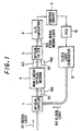
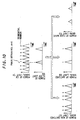
- Fig. 1 shows an apparatus for extracting a clock light in the first preferred embodiment according to the invention.
- the apparatus comprises an optical coupler 1, an optical non-linear medium 4, an optical filter 5, an optoelectric (O/E) converter 8, a control circuit 9, a voltage controlled oscillator (VCO) 10, and a clock light generator 11.
- O/E optoelectric
- VCO voltage controlled oscillator
- a signal light 101 which is supplied to the optical coupler 1 is a pulse-coded signal into which an output light of a semiconductor laser lasing with a single mode is modulated to have a data rate of 20 Gb/s, a mark ratio of 1/2, and a pulse width of 25ps in the form of RZ code by a LiNbO3 optical modulator, and a clock light 102 which is also supplied to the optical coupler 1 has a repetition frequency of 20 GHz, and a pulse width of 25ps which are the same as those in the signal light 1.
- the clock light 102 is generated in the clock light generator 11 utilizing a gain switch as a pulse light source to be driven by an electric signal of an oscillation frequency of 20GHz supplied from the VCO 10.
- the signal light 101 having a wavelength ⁇ s of 1.554 ⁇ m and the clock light 102 having a wavelength ⁇ c of 1.550 ⁇ m are combined by the optical coupler 1, from which an output light is incident to the non-linear optical medium 4 which is a silica-based single mode optical fiber having a length of 10 km and a zero-dispersion wavelength of 1.552 ⁇ m.
- the peak powers of the signal and clock lights 101 and 102 are set to be +40mW at the input of the non-linear optical medium 4, in which four-wave mixing occurs to provide to four-wave mixing lights 103 having wavelength ⁇ m1 and ⁇ m2 of 1.546 ⁇ m (2 ⁇ c - ⁇ s) and 1.558 ⁇ m (2 ⁇ s - ⁇ c) as output lights thereof along with the signal and clock lights 101 and 102.
- the output lights of the non-linear optical medium 4 only the four-wave mixing light 103 of the wavelength ⁇ m1 passes through the optical filter 5.
- the four-wave mixing light 103 is extracted.
- the extracted four-wave mixing light 103 is received to be supplied as an electric signal to the control circuit 9 by the O/E converter 8, from which a control signal is supplied to the VCO 10.
- an optical phase locked loop optical PLL
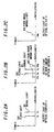
- Fig. 2A shows the signal and clock lights 101 and 102 ( ⁇ c and ⁇ s) supplied from the optical coupler 1
- Fig. 2B shows the signal and clock lights 101 and 102 ( ⁇ c and ⁇ s) and the four-wave mixing lights 103 ( ⁇ m1 and ⁇ m2) supplied from the non-linear optical medium 4
- Fig. 2C shows the four-wave mixing light 103 ( ⁇ m1) extracted by the optical filter 5.
- the power of the four-wave mixing light 103 is dependent on a phase difference ⁇ between the signal and clock lights 101 and 102 as shown in Figs. 3A to 3D.
- Fig. 3A shows the case where the phase difference ⁇ is zero between the signal and clock lights 101 and 102, so that the power of the four-wave mixing light 103 is maximum
- Fig. 3B shows the case where the phase difference ⁇ is ⁇ /2 therebetween, so that the power of the four-wave mixing light 103 is lowered as compared to the maximum value
- Fig. 3C shows the case where the phase difference ⁇ is ⁇ , so that the power of the four-wave mixing light 103 is minimum.
- the phase lock between the signal and clock lights 101 and 102 is obtained by converting the four-wave mixing light 103 to an electric signal in the O/E converter 8 and feeding the electric signal via the control circuit 9 to the VCO 10.
- phase differences of the clock light 102 and an electric clock signal for generating the clock light 102 relative to the signal light 101 are maintained to be constant even in the case where the frequency of a clock signal in a signal source for driving the LiNbO3 optical modulator is fluctuated to some extent.
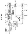
- Fig. 4A shows an apparatus for extracting a clock light in the second preferred embodiment according to the invention, wherein like parts are indicated by like reference numerals as used in Fig. 1, and the apparatus further comprises an oscillator 19, a mixer 20, and a phase modulator 21.
- a signal light 101 which is supplied to the optical coupler 1 is a pulse coded signal into which an output light of a semiconductor laser lasing with a signal mode is modulated to have a data rate of 20 Gb/s, a mark ratio of 1/2, and a pulse width of 20ps in the form of RZ code by LiNbO3 optical modulator
- a clock light which is also supplied to the optical coupler 1 is an intensity-modulated signal into which an output light of a semiconductor laser lasing with a single mode is modulated to have a repetition frequency of 20GHz which is the same as the clock frequency of 20GHz for the signal light 101 by a LiNbO3 optical modulator.
- the clock generator 11 is driven by an electric output signal of an oscillator frequency of 20GHz supplied from the VCO 10, wherein the output signal of the VCO 10 is phase modulated by the phase modulator 21 which is driven by an oscillation frequency of 100kHz supplied from the oscillator 19.
- the signal light 101 having a wavelength ⁇ s of 1.554 ⁇ m and the clock light 102 having a wavelength ⁇ c of 1.550 ⁇ m are combined in the optical coupler 1.
- one of the four-wave mixing lights 103 passes through the optical filter 5.
- the extracted four-wave mixing light 103 is converted to an electric signal in the O/E convertor 8, and the electric signal is supplied to the mixer 20 together with an output signal of the oscillator 19.
- the generator voltage is supplied from the mixer 20 to the control circuit 9, form which a control signal is supplied to the VCO 10.
- an optical phase locked loop optical PLL
- the time-mean value of power for the four-wave mixing light 103 is maximum in case of the phase difference of zero between the signal and clock lights 101 and 102, and minimum in case of the phase difference of ⁇ therebetween.
- phase modulator 21 a signal of 100kHz is superposed to the output signal of the VCO 10, so that the phase modulation of a repetition frequency 100kHz is applied to the clock light 102.
- the phase-modulation component is represented on the four-wave mixing light 103, so that the phase difference ⁇ is detected between the signal and clock lights 101 and 102 by the synchronous detection in the mixer (phase comparator) 20 supplied with output signals of the O/E converter 8 and the oscillator 19.
- the output signal of the mixer 20 is supplied via the control circuit 9 to the VCO 10, so that the phase lock between the signal and clock lights 101 and 102 is realized.
- the timing extracting apparatus in the second preferred embodiment, it is confirmed that the clock light 102 and a related electric clock signal are locked in phase to the signal light 101, even if a clock frequency of a signal source for driving the LiNbO3 optical modulator is fluctuated to some extent.
- Fig. 5 shows an apparatus for extracting a clock light in the third preferred embodiment according to the invention, wherein like parts are indicated by like reference numerals as used in Fig. 4, and the clock light generator 11 comprises a semiconductor laser 13, a LiNbO3 optical modulator 14, a drive circuit 15, a resistance 16, and bias circuit 17 and 18.
- the signal light 101 is the same as one used in the first and second preferred embodiments, and the clock light 102 is generated in the clock light generator 11 which an output light of the semiconductor laser 13 lasing with a signal mode is intensity-modulated in the LiNbO3 optical modulator 14 which is driven by the drive circuit 15, and a frequency of the clock light 102 is the same as that of the signal light 101.
- the two bias circuits 17 and 18 are used to superpose an intensity modulation signal of 100kHz on the clock light 102.
- the first bias circuit 17 biases the clock light 102 of 20 GHz
- the second bias circuit 18 biases an output signal of 100kHz supplied from the oscillator 19.
- the first bias circuit 17 is connected via the resistance 16 of 50 ⁇ to ground.
- the signal light 101 having a wavelength ⁇ s of 1.554 ⁇ m and the clock light 102 having a wavelength ⁇ c of 1.550 ⁇ m are combined in the optical coupler 1, from which the combined signal and clock lights 101 and 102 are supplied to the non-linear optical medium 4 of a silica-based single mode optical fiber having a length of 10km and a zero-dispersion wavelength of 1.552 ⁇ m, wherein the input peak power levels of the signal and clock lights 101 and 102 are set to be +40mW.
- the four-wave mixing light 103 having the wavelength ⁇ m1 passes through the optical filter 5 to be converted to an electric signal in the O/E converter 8.
- the output signals of the O/E converter 8 and the oscillator 19 are supplied to the mixer 20, in which a voltage is generated dependency on a phase difference between the signal and clock lights 101 and 102.
- the output signal of the mixer 20 is supplied to the control circuit 9, from which a control signal is fed back to the VCO 10.
- an optical PLL is structured.
- the signal of 100kHz which is the output signal of the oscillator 19 is superposed on the LiNbO3 optical modulator 14, so that the intensity-modulation of 100kHz is superposed on the clock light 102.
- This intensity-modulation component is represented on the four-wave mixing light 103. Therefore, the output signal of the O/E converter 8 and the oscillator 19 are supplied to the mixer 20 to carry out the synchronous detection, so that a phase difference ⁇ is detected between the signal and clock lights 101 and 102.
- the output signal of the mixer 20 is supplied via the control circuit 9 to the VCO 10, thereby to lock the signal and clock lights 101 and 102 in phase.
- Fig. 6 shows an apparatus for demultiplexing an optical time-division multiplexed signal in the first preferred embodiment according to the invention.
- the apparatus comprises optical couplers 1 and 2, a non-linear optical medium 4, an optical filter 5, an O/E converter 8, a control circuit 9, a VCO 10, and a clock light generator 11.
- a signal light 101 is a signal having a data rate of 40Gb/s which is obtained by multiplexing in time-division four sequential signals.
- Each of the four sequential signals is obtained by dividing into four signals a short pulse having a repetition frequency of 10GHz and a pulse width of 10ps. generated by a gain switch of a semiconductor laser, and by modulating each of the four-divided signals to have a data rate of 10GHz, a mark ratio of 1/2 and a pulse width of 10ps in the form of RZ code by a LiNbO3 optical modulator.
- an appropriate time difference is assigned between adjacent sequential signals by an optical variable delay device which is an optical fiber stretcher, and the sequential signals thus processed are combined not to overlap on each other by an optical coupler.
- the clock light 102 has a repetition frequency of 10GHz which is one quarter of the clock frequency of the signal light 101 and equal to the clock frequency of the sequential signals to be combined, and a pulse width of lops equal to that of the signal light 101.
- the clock light 102 as explained above is generated in the clock light generator 11 which is driven by an electric signal of an oscillation frequency of 10GHz supplied from the VCO 10 and comprises a gain switch of a semiconductor laser for a pulse light source.
- the signal light 101 having a wavelength ⁇ s of 1.554 ⁇ m and the clock light 102 having a wavelength ⁇ c of 1.550 ⁇ m are combined in the first optical coupler 1, from which the combined signal and clock lights 101 and 102 are supplied to the non-linear optical medium 4 of a silica-based single mode optical fiber having a length 10km and a zero-dispersion wavelength of 1.552 ⁇ m.
- the four-wave mixing light 103 having the wavelength ⁇ m1 is only passed through the optical filter 5, and is divided into two four-wave mixing lights by the second optical coupler 2.
- One of the two divided light is an output light, while the other divided light is supplied to the O/E converter 8, from which an electric signal is supplied to the control circuit 9.
- an optical PLL is structured.
- Fig. 7 shows the signal light 101 which comprises first to fourth sequential lights as numbered by 1 to 4, and the clock light 102 which is coincident with the first sequential signal 1 in case of no phase difference therebetween. Consequently, the four-wave mixing light 103 is generated at a timing common to those of the first sequential signal for the signal light 101 and the clock light 102.
- the phase lock of the clock light 102 to the signal light 102 to the signal light 101 is realized, and one sequential signal of 10GHz is demultiplexed from the signal light 101 of 40GHz which is multiplexed by the first to fourth sequential signals.
- Fig. 8 shows an apparatus for demultiplexing a time-division multiplexed signal in the second preferred embodiment according to the invention.
- the demultiplexing apparatus comprises optical couplers 1, 2 and 3, a non-linear optical medium 4, optical filters 5 and 6, an O/E converter 8, a control circuit 9, a VCO 10 and a clock light generator 11.
- a signal light 1 which is the same as one in the first preferred embodiment is supplied to a port 1 of the optical fiber type first optical coupler 1 to be divided into two signal lights at ports 3 and 4 thereof.
- the signal light 104 of the clockwise (CW) direction supplied from the port 3 of the first optical coupler 1 and a clock light 102 which is the same as one in the first preferred embodiment are combined in the second optical coupler 2, from which output lights are supplied to the non-linear optical medium 4 of a silica-based single mode optical fiber having a length of.lOkm and a zero-dispersion wavelength of 1.552 ⁇ m, at the input of which peak power levels of the signal and clock lights 104 and 102 are set to be +40mW.
- four-wave mixing occurs in accordance with the CW signal light 104 and the clock light 102.
- the CW clock light 102, the CW four-wave mixing light 103, and the CW signal light 104 are supplied to the port 4 of the optical coupler 1, while the signal light 105 of counter clockwise (CCW) direction supplied from the port 4 of the optical coupler 1 propagates through the non-linear optical medium 4 to arrive at the port 3 of the optical coupler 1.
- CCW counter clockwise
- the CW and CCW signal lights 104 and 105 supplied to the ports 4 and 3 of the optical coupler 1 are interfered with each other, and the interfered light is obtained at the port 1 of the optical coupler 1 in case of zero in phase difference between the CW and CCW signal lights 104 and 105, and at the port 2 thereof in case of ⁇ in phase difference therebetween.
- the interfered light obtained at the port 1 is a non-switched signal light 107 which is subject to no phase shift for the CW signal light 104 induced by the clock light 102
- the interfered light obtained at the port 2 is a switched light 106 which is subject to a phase shift of ⁇ for the CW signal light 104 induced by the clock light 102.
- the clock light 102 and the four-wave mixing light 103 are respectively divided into two lights by the optical coupler 1. Consequently, the lights supplied from the port 1 of the optical coupler 1 are the non-switched signal light 107, the clock light 102, and the four-wave mixing light 103, from which only the non-switched signal light 107 is extracted to be supplied to a next stage for demultiplexing a time-division multiplexed signal by an optical filter.
- the light supplied from the port 2 of the optical coupler 1 are the switched light 106, the clock light 102, and the four-wave mixing light 103 which are respectively divided into two lights, from one of which only the four-wave mixing light 103 is extracted by the first optical filter 5, and from the other one of which only the switched signal light 106 is extracted by the second optical filter 6.
- the output light of the first optical filter 5 is received in the O/E converter 8 to provide on electric signal which is supplied to the control circuit 9, from which a control signal is supplied to the VCO 10.
- Figs. 9A to 9D the CW signal light 104 of the wavelength ⁇ s and the clock light 102 of the wavelength ⁇ c supplied from the second optical coupler 2 are shown, and, in Fig. 9B, the CW signal and clock lights 104 and 102, and the four-wave mixing lights 103 of the wavelengths ⁇ m1 and ⁇ m2 are shown as output lights of the non-linear optical medium 4. Then, the clock light 102, the CW signal light 106, and the four-wave mixing light 103 are obtained from the port 2 of the first optical coupler 1, as shown in Fig. 9C, and the four-wave mixing light 103 of the wavelength ⁇ m1 is only obtained from the optical filter 5, as shown in Fig. 9D.
- the CW signal light 104 comprises four time sequential signals as numbered by 1 to 4, and the clock light 102 has a repetition frequency of one quarter of the frequency of the CW signal light 104.
- the clock light 102 is in phase with the sequential signal 1 of the CW signal light 104 (corresponding to one of four time slots). Consequently, the switched signal light 106 (the sequential signals 19 is obtained at the port 2 of the optical coupler 1, and the non-switched signal light 107 (sequential signals 2 to 4) is obtained at the port 1 of the optical coupler 1, respectively, as shown thereof.
- Fig. 10 also shows the four-wave mixing light 103 supplied from the optical filter 5.
- the clock light 102 may be in phase with any one of the sequential signal 2 to 4 in case of no phase difference between the signal light 101 and the clock light 102.
- Fig. 11 shows an apparatus for demultiplexing a time-division multiplexed signal in the third preferred embodiment according to the invention.
- the demultiplexing apparatus comprises optical couplers 1 and 2, a non-linear optical medium 4, optical filters 5 and 6, an O/E converter 8, a control circuit 9, an VCO 10, a clock light generator 11, and a polarization beam splitter 12.
- a signal light 101 and a clock light 102 are combined in the first optical coupler 1 to be supplied to the non-linear optical medium 4 of a silica-based single mode optical fiber having a length of 10km and a zero-dispersion wavelength of 1.552 ⁇ m under the same condition as in the first preferred embodiment.
- a peak power of the signal light 101 is set to be +4mW, and that of. the clock light 102 is set to be +50mW.
- the output lights of the non-linear optical medium 4 are respectively divided into two lights, from one of which only the signal light 101 is extracted by the first optical filter 5, and from the other one of which the four-wave mixing light 103 is extracted by the second optical filter 6.
- the signal light 101 is supplied from the first optical filter 5 to the polarization beam splitter 12, from which a switched signal light 106 and a non-switched signal light 107 are separately obtained.
- the four-wave mixing light 103 is supplied from the second optical coupler 6 to the O/E converter 8, from which an electric signal is supplied to a control circuit 9. Then, a control signal is supplied from the control circuit 9 to the VCO 10.
- the timing extracting operation is the same as one in the first preferred embodiment.
- the phenomenon in which phase shift amounts induced by cross phase modulation of a polarization component of the signal light 101 parallel to the clock light 102 and a polarization component of the signal light 101 thereto are different is used.
- a phase difference of the two components is ⁇
- the signal light 101 is rotated in polarization between the input and the output of the non-linear optical medium 4 by 90°.
- the signal light 106 which is switched by the clock light 102 and the signal light 107 which is not switched by the clock light 102 are obtained from the polarizing beam splitter 12.
- the clock light 102 is locked in phase to the signal light 101, and a time sequential signal of 10Gb/s is obtained from the signal light 101 of 40Gb/s which is multiplexed in time-division.
- Fig. 12 shows an apparatus for demultiplexing a time-division multiplexed signal in the fourth preferred embodiment according to the invention.
- the demultiplexing apparatus comprises optical couplers 1, 2 and 3, a non-liner optical medium 4, optical filters 5, 6 and 7, an O/E converter 8, a control circuit 9, a VCO 10, and a clock light generator 11.
- the signal light 101 is set to be +4mW in peak power level at the input of the non-linear optical medium, and the clock light 102 is set to be +40mW in peak power level thereat.
- the timing extracting operation is similar to that in the first to third preferred embodiments, and the demultiplexing operation is carried out by utilizing a phase shift of the signal light 101 induced by cross phase modulation relative to the clock light 102.
- the phase shift amount is ⁇
- the signal lights 101 supplied from the second and third optical filters 6 and 7 are interfered in the third optical coupler 3 to provide a signal light 106 which is switched by the clock light 102 at one port of the third optical coupler 3 and to provide a signal light 107 which is not switched by the clock light 102 at the other port thereof.
- the structure may be modified as set out below.
- the non-linear optical medium 4 is not limited to a silica-based single mode optical fiber, but it may be a semiconductor optical amplifier, an inorganic or organic having third order non-linear optical effect. Further, a polarization maintaining optical fiber or other optical fibers may be used for the non-linear optical medium. In such an optical fiber, the zero-dispersion wavelength may be 1.56 ⁇ m, 1.3 ⁇ m, or other wavelength under the condition where the non-linear optical effect is sufficiently obtained by. the signal and clock lights 101 and 102.
- the peak power levels of the signal and clock lights 101 and 102 may be +20mW, +40mW, or other values at the input of the non-linear optical medium 4, if the nonlinear optical effect is generated.
- the optical power may be amplified by using an Er-doped optical fiber or a semiconductor optical amplifier as the non-linear optical medium 4, if the non-linear optical effect is sufficiently obtained.
- An optical amplifier may be used at an appropriate position for amplification purpose.
- the wavelength of the signal or clock light 101 or 102 may be 1.3 ⁇ m, 1.555 ⁇ m, or other values.
- the signal light 101 may be modified as set out below. That is, the data bit may 5Gb/s or 100Gb/s.
- the number of time-division multiplexing signals is not limited to 4, and may be 2 or 10.
- NRZ coding may be used in place of RZ coding.
- the mark ratio is not limited to 1/2, and may be 3/8 or 1/8.
- the pulse width is not limited to 25ps or 10ps, and may be 100ps or 5ps, if it is less than one time slot of a clock frequency of the signal light 101.
- the form of pulse may be a short pulse having a small duty ratio, a sine-wave pulse, or other forms, if it is functions as a signal light.
- the extinction ratio may be 10dB, or 20dB.
- the clock light 102 may be modified as set out below.
- the division ratio of the clock frequency of the clock light 102 relative to the clock frequency of the signal light 101 is not limited to 4, and may be 2 or 20.
- the clock frequency of the clock light 102 may be a value multiplexing the clock frequency of the signal light 101.
- the same things as in the signal light 101 are applied to the pulse width, the pulse form, the extinction ratio, etc. of the clock light 102.
- An optical fiber squeezer may be used to control at least one of polarization of the signal and clock lights 101 and 102, so that the maximum non-linear optical effect is obtained dependent on polarizations.
- a light received by the O/E converter 8 is not limited to the four-wave mixing light 103, but it may be the signal or clock light 101 or 102, a power time-mean value of the light 101 or 102 is reduced at the output of the nonlinear optical medium 4 due to the generation of the four-wave mixing light 103.
- the minimum value may be controlled to maximize the overlapping degree of the signal and clock lights 101 and 102 by the control circuit 10 in the demultiplexing apparatus.
- the optical couplers 1, 2 and 3 may be a reflection film type or other type in place of an optical fiber type.
- the optical filters 5, 6 and 7 may be an interference film type, a Fabry Perot type, or other types.
- the O/E converter 8 may be a p-i-n photodiode, an avalanche photodiode, or other types.
- a pulse light source in the clock light generator 11 is not. limited to a semiconductor laser using a gain switch, but it may be modified as set out below. That is, it may be a semiconductor laser using a mode lock as a short pulse generator, a ring laser, or other devices which are driven to provide appropriate repetition frequency and pulse width by an output signal of the VCO 10.
- a repetition frequency is generated by branching a light in an optical coupler, applying a delay to the branched light, and combining the delayed light to a light from the light source, and a pulse width is regulated by the pulse compression technology using grating pair, or using high order soliton.
- the clock pulse 102 is not limited to a short pulse light, and it may be an intensity modulation light which is normally obtained by an external modulator such as the LiNbO3 optical modulator 14 and an electric field absorption type semiconductor optical modulator, wherein the intensity modulation index is not limited, if the non-linear optical effect is obtained.
- the oscillation frequency of 100kHz in the oscillator 19 may be changed to be, for instance, 1MHz, or 10kHz, if synchronous detection is realized.
- the non-linear switch used in the demultiplexing apparatus is not limited to a non-linear optical fiber loop mirror, an optical Kerr switch, or other types using the signal and clock lights 101 and 102 having different. wavelengths.
- timing extracting apparatus As described above, advantages of the timing extracting apparatus and the demultiplexing apparatus are summarized below.
Landscapes
- Physics & Mathematics (AREA)
- Optics & Photonics (AREA)
- Engineering & Computer Science (AREA)
- Computer Networks & Wireless Communication (AREA)
- Signal Processing (AREA)
- Optical Communication System (AREA)
- Synchronisation In Digital Transmission Systems (AREA)
Applications Claiming Priority (3)
| Application Number | Priority Date | Filing Date | Title |
|---|---|---|---|
| JP83179/93 | 1993-04-09 | ||
| JP8317993 | 1993-04-09 | ||
| JP8317993A JPH0813025B2 (ja) | 1993-04-09 | 1993-04-09 | 光クロック抽出装置及び光時分割多重分離装置 |
Publications (3)
| Publication Number | Publication Date |
|---|---|
| EP0619658A2 true EP0619658A2 (fr) | 1994-10-12 |
| EP0619658A3 EP0619658A3 (en) | 1995-12-06 |
| EP0619658B1 EP0619658B1 (fr) | 2004-12-08 |
Family
ID=13795078
Family Applications (1)
| Application Number | Title | Priority Date | Filing Date |
|---|---|---|---|
| EP94302513A Expired - Lifetime EP0619658B1 (fr) | 1993-04-09 | 1994-04-11 | Dispositif pour l'extraction d'une horloge optique et dispositif pour le démultiplexage d'un signal multiplexé par division du temps |
Country Status (4)
| Country | Link |
|---|---|
| US (1) | US5457559A (fr) |
| EP (1) | EP0619658B1 (fr) |
| JP (1) | JPH0813025B2 (fr) |
| DE (1) | DE69434167T2 (fr) |
Cited By (6)
| Publication number | Priority date | Publication date | Assignee | Title |
|---|---|---|---|---|
| EP0657765A1 (fr) * | 1993-12-04 | 1995-06-14 | Alcatel SEL Aktiengesellschaft | Mélangeur optique et son utilisation |
| EP0774844A1 (fr) * | 1995-11-14 | 1997-05-21 | PIRELLI CAVI S.p.A. | Méthode et dispositif pour la récupération optique du synchronisme d'un signal numérique optique |
| WO1997044929A1 (fr) * | 1996-05-22 | 1997-11-27 | British Telecommunications Public Limited Company | Dispositif de synchronisation optique |
| FR2774832A1 (fr) * | 1998-02-12 | 1999-08-13 | Alsthom Cge Alcatel | Procede et dispositif de resynchronisation de signaux optiques |
| EP1119119A1 (fr) * | 2000-01-20 | 2001-07-25 | Nippon Telegraph and Telephone Corporation | Générateur de signal local avec PLL pour synchroniser la phase d'horloge avec une suite de signaux optiques |
| EP1185007A3 (fr) * | 2000-09-01 | 2009-08-19 | Fujitsu Limited | Procédé, dispositif et système de traitement de signaux optiques |
Families Citing this family (30)
| Publication number | Priority date | Publication date | Assignee | Title |
|---|---|---|---|---|
| US5574588A (en) * | 1994-02-23 | 1996-11-12 | Nippon Telegraph And Telephone Corporation | Phase lock loop circuit using optical correlation detection |
| DE69526342T2 (de) * | 1994-05-23 | 2002-10-31 | British Telecommunications P.L.C., London | Verarbeitung optischer pakete |
| JP3846918B2 (ja) * | 1994-08-02 | 2006-11-15 | 富士通株式会社 | 光伝送システム、光多重伝送システム及びその周辺技術 |
| DE69534362T2 (de) * | 1994-08-15 | 2006-05-24 | Nippon Telegraph And Telephone Corp. | Volloptischer mehrkanaliger TDM-WDM Konverter und volloptischer mehrkanaliger Zeit-Demultiplexer |
| US5612973A (en) * | 1995-06-19 | 1997-03-18 | Massachusetts Institute Of Technology | System employing dissipative pseudorandom dynamics for communications and measurement |
| US5825519A (en) * | 1996-09-27 | 1998-10-20 | Princeton University | Optical mach-zehnder time division demultiplexer |
| GB2320635A (en) * | 1996-12-19 | 1998-06-24 | Northern Telecom Ltd | Optical timing detection using an interferometer |
| US6020839A (en) * | 1997-10-27 | 2000-02-01 | Int Labs, Inc. | Analog technique to detect asymmetric radio frequency pulses |
| KR20000037800A (ko) | 1998-12-02 | 2000-07-05 | 정선종 | 편광에 무관한 광 역다중화기 |
| US7155095B2 (en) * | 1999-03-29 | 2006-12-26 | Furukawa Electric Co., Ltd. | Method for efficient four-wave mixing generation and short pulse generation equipment using the method |
| JP3732371B2 (ja) * | 1999-09-09 | 2006-01-05 | 沖電気工業株式会社 | 光信号発生回路 |
| US6501579B2 (en) * | 2000-03-03 | 2002-12-31 | Optium, Inc. | Apparatus, system, and method for extracting an optical clock signal from an optical data signal |
| US7068946B2 (en) | 2001-01-23 | 2006-06-27 | At&T Corp. | Modulation scheme for tedons |
| JP4801281B2 (ja) * | 2001-05-31 | 2011-10-26 | 富士通株式会社 | 光パルス挿入装置 |
| DE10137874B4 (de) * | 2001-08-02 | 2004-02-26 | Siemens Ag | Add-Drop Multiplexer für OTDM-Signale |
| DE10214927B4 (de) * | 2002-04-04 | 2004-02-26 | Siemens Ag | Verfahren zum Aufteilen eines optischen Datensignals in n elektrische Datensignale mit niedrigerer Bitrate |
| DE60225116T2 (de) * | 2002-04-24 | 2009-02-19 | Alcatel Lucent | Remodulator für optische Übertragungssysteme |
| KR100475850B1 (ko) * | 2002-10-08 | 2005-03-10 | 한국전자통신연구원 | 광 필터를 사용한 클럭 추출 방법 및 장치 |
| US7302728B2 (en) * | 2004-03-11 | 2007-12-04 | Coe Kunz | Cleaning implement for golfers |
| JP2005348127A (ja) * | 2004-06-03 | 2005-12-15 | Yokogawa Electric Corp | 光クロック信号抽出装置 |
| JP4342393B2 (ja) * | 2004-07-14 | 2009-10-14 | 株式会社東芝 | 携帯端末機器に装着される電子装置及び電子装置の制御方法 |
| JP4476097B2 (ja) * | 2004-10-28 | 2010-06-09 | 富士通株式会社 | クロック抽出方法および装置 |
| ITMI20042312A1 (it) * | 2004-12-01 | 2005-03-01 | Marconi Comm Spa | Multiplexer con add-drop ottico |
| JP5410534B2 (ja) * | 2008-10-14 | 2014-02-05 | コーネル・ユニバーシティー | 位相シフトを入力波形に対して付与する装置 |
| CN102388298B (zh) * | 2009-02-05 | 2013-10-23 | 康奈尔大学 | 通过使用四波混频进行时间展宽的高速光采样 |
| US8275263B1 (en) * | 2009-06-26 | 2012-09-25 | The Boeing Company | Multiplication of phase deviations |
| US9088369B2 (en) | 2012-12-28 | 2015-07-21 | Synergy Microwave Corporation | Self injection locked phase locked looped optoelectronic oscillator |
| JP6128134B2 (ja) * | 2013-01-21 | 2017-05-17 | 富士通株式会社 | 周波数変換装置、波長多重装置および周波数変換方法 |
| US9094133B2 (en) * | 2013-03-12 | 2015-07-28 | Synergy Microwave Corporation | Integrated production of self injection locked self phase loop locked optoelectronic oscillator |
| US10256912B2 (en) * | 2014-03-04 | 2019-04-09 | National Institute Of Advanced Industrial Science And Technology | Optical phase regeneration method and device |
Family Cites Families (2)
| Publication number | Priority date | Publication date | Assignee | Title |
|---|---|---|---|---|
| US4980891A (en) * | 1989-12-22 | 1990-12-25 | Bell Communications Research, Inc. | Clocked optical regenerator and other optoelectronic functional circuits |
| JP2701608B2 (ja) * | 1991-07-29 | 1998-01-21 | 日本電気株式会社 | 光クロック抽出回路 |
-
1993
- 1993-04-09 JP JP8317993A patent/JPH0813025B2/ja not_active Expired - Fee Related
-
1994
- 1994-04-11 DE DE69434167T patent/DE69434167T2/de not_active Expired - Fee Related
- 1994-04-11 EP EP94302513A patent/EP0619658B1/fr not_active Expired - Lifetime
- 1994-04-11 US US08/225,589 patent/US5457559A/en not_active Expired - Lifetime
Non-Patent Citations (3)
| Title |
|---|
| ELECTRONICS LETTERS, vol. 28, no. 5, XP 000292706 KAWANISHI S ET AL '10GHZ TIMING EXTRACTION FROM RANDOMLY MODULATED OPTICAL PULSES USING PHASE-LOCKED LOOP WITH TRAVELLING-WAVE LASER-DIODE OPTICAL AMPLIFIER USING OPTICAL GAIN MODULATION' * |
| ELECTRONICS LETTERS, vol. 29, no. 2, 21 January 1993 STEVENAGE GB, pages 231-233, XP 000331631 S. KAWANISHI ET AL. '64 to 8 Gbit/s ALL-OPTICAL DEMULTIPLEXING EXPERIMENT WITH CLOCK RECOVERY USING NEW PHASE LOCK LOOP TECHNIQUE' * |
| OFC '94. OPTICAL FIBER COMMUNICATION. VOL.4. 1994 TECHNICAL DIGEST SERIES. CONFERENCE EDITION (IEEE CAT. NO.94CH3422-3), 1994 CONFERENCE ON OPTICAL FIBER COMMUNICATION - OFC'94, SAN JOSE, CA, USA, 20-25 FEB. 1994, ISBN 1-55752-321-5, 1994, WASHINGTON, DC, USA, OPT. SOC. AMERICA, USA, pages 61-62, SAITO T ET AL '10-GHz timing extraction from a 20-Gbit/s optical data stream by using a newly proposed optical phase-locked loop' * |
Cited By (13)
| Publication number | Priority date | Publication date | Assignee | Title |
|---|---|---|---|---|
| US5504610A (en) * | 1993-12-04 | 1996-04-02 | Alcatel N.V. | Optical mixer and its use |
| EP0657765A1 (fr) * | 1993-12-04 | 1995-06-14 | Alcatel SEL Aktiengesellschaft | Mélangeur optique et son utilisation |
| EP0774844A1 (fr) * | 1995-11-14 | 1997-05-21 | PIRELLI CAVI S.p.A. | Méthode et dispositif pour la récupération optique du synchronisme d'un signal numérique optique |
| US5777766A (en) * | 1995-11-14 | 1998-07-07 | Pirelli Cavi S.P.A. | Method and device for optically recovering the synchronism of an optical digital signal |
| US6137610A (en) * | 1996-05-22 | 2000-10-24 | British Telecommunications Public Limited Company | Optical synchronization arrangement |
| WO1997044929A1 (fr) * | 1996-05-22 | 1997-11-27 | British Telecommunications Public Limited Company | Dispositif de synchronisation optique |
| AU735930B2 (en) * | 1996-05-22 | 2001-07-19 | British Telecommunications Public Limited Company | Optical synchronisation arrangement |
| EP0936773A1 (fr) * | 1998-02-12 | 1999-08-18 | Alcatel | Procédé et dispositif de resynchronisation de signaux optiques |
| FR2774832A1 (fr) * | 1998-02-12 | 1999-08-13 | Alsthom Cge Alcatel | Procede et dispositif de resynchronisation de signaux optiques |
| US6424443B1 (en) | 1998-02-12 | 2002-07-23 | Alcatel | Optical signal resynchronization method and device |
| EP1119119A1 (fr) * | 2000-01-20 | 2001-07-25 | Nippon Telegraph and Telephone Corporation | Générateur de signal local avec PLL pour synchroniser la phase d'horloge avec une suite de signaux optiques |
| US6560007B2 (en) | 2000-01-20 | 2003-05-06 | Nippon Telegraph And Telephone Corporation | Bit-phase synchronized optical pulse stream local generator |
| EP1185007A3 (fr) * | 2000-09-01 | 2009-08-19 | Fujitsu Limited | Procédé, dispositif et système de traitement de signaux optiques |
Also Published As
| Publication number | Publication date |
|---|---|
| US5457559A (en) | 1995-10-10 |
| DE69434167D1 (de) | 2005-01-13 |
| EP0619658B1 (fr) | 2004-12-08 |
| DE69434167T2 (de) | 2005-12-01 |
| JPH0813025B2 (ja) | 1996-02-07 |
| EP0619658A3 (en) | 1995-12-06 |
| JPH06303216A (ja) | 1994-10-28 |
Similar Documents
| Publication | Publication Date | Title |
|---|---|---|
| US5457559A (en) | Apparatus for extracting an optical clock and apparatus for demultiplexing a time-division multiplexed signal | |
| US7110677B2 (en) | Method and system for optical time division multiplexed fiber communications with coherent detection | |
| US5892608A (en) | Optical receiver device for dark soliton lightwave | |
| US7224906B2 (en) | Method and system for mitigating nonlinear transmission impairments in fiber-optic communications systems | |
| US5574588A (en) | Phase lock loop circuit using optical correlation detection | |
| EP1170627B1 (fr) | Porte optique et modulateur de phase optique | |
| Fice et al. | Homodyne coherent optical receiver using an optical injection phase-lock loop | |
| US20030020985A1 (en) | Receiver for high-speed optical signals | |
| JPH09325308A (ja) | 光変調器、短光パルス発生装置、光波形整形装置および光デマルチプレクサ装置 | |
| US6940638B2 (en) | Optical frequency conversion systems and methods | |
| US6239893B1 (en) | Very high data rate soliton regenerator | |
| US7356220B2 (en) | Apparatus and method for reducing signal noise and OCDMA receiver and method | |
| US20050018271A1 (en) | Apparatus for simultaneous OTDM demultiplexing, electrical clock recovery and optical clock generation, and optical clock recovery | |
| JP3556657B2 (ja) | 位相共役光学の光システムへの適用 | |
| JP3476806B2 (ja) | 位相共役光学の光システムへの適用 | |
| Yamamoto et al. | 160 Gbit/s demultiplexer with clock recovery using SOA-based interferometric switches and its application to 120 km fiber transmission | |
| EP1427125A2 (fr) | Méthode et dispositif de séparation des impulsions optiques | |
| Tokle et al. | Wavelength conversion of 80 Gbit/s optical DQPSK using FWM in a highly non-linear fibre | |
| Kawanishi et al. | Time-division-multiplexed 100 Gbit/s, 200 km optical transmission experiment using PLL timing extraction and all-optical demultiplexing based on polarization insensitive four-wave-mixing | |
| JP3576546B2 (ja) | 位相共役光学の光システムへの適用 | |
| JPH09102776A (ja) | 光クロック信号抽出回路 | |
| JP3280185B2 (ja) | 時分割多重光信号の多重分離方法及びその装置 | |
| JP3386090B2 (ja) | 光クロック位相同期ループ回路 | |
| WO2003036834A1 (fr) | Procede et systeme de communications optiques par fibre a multiplexage temporel avec detection coherente | |
| JP2005269667A (ja) | 光伝送システム、光多重伝送システム及びその周辺技術 |
Legal Events
| Date | Code | Title | Description |
|---|---|---|---|
| PUAI | Public reference made under article 153(3) epc to a published international application that has entered the european phase |
Free format text: ORIGINAL CODE: 0009012 |
|
| AK | Designated contracting states |
Kind code of ref document: A2 Designated state(s): DE FR GB |
|
| PUAL | Search report despatched |
Free format text: ORIGINAL CODE: 0009013 |
|
| AK | Designated contracting states |
Kind code of ref document: A3 Designated state(s): DE FR GB |
|
| 17P | Request for examination filed |
Effective date: 19951020 |
|
| 17Q | First examination report despatched |
Effective date: 19991209 |
|
| GRAP | Despatch of communication of intention to grant a patent |
Free format text: ORIGINAL CODE: EPIDOSNIGR1 |
|
| GRAA | (expected) grant |
Free format text: ORIGINAL CODE: 0009210 |
|
| GRAS | Grant fee paid |
Free format text: ORIGINAL CODE: EPIDOSNIGR3 |
|
| AK | Designated contracting states |
Kind code of ref document: B1 Designated state(s): DE FR GB |
|
| REG | Reference to a national code |
Ref country code: GB Ref legal event code: FG4D |
|
| REF | Corresponds to: |
Ref document number: 69434167 Country of ref document: DE Date of ref document: 20050113 Kind code of ref document: P |
|
| PLBE | No opposition filed within time limit |
Free format text: ORIGINAL CODE: 0009261 |
|
| STAA | Information on the status of an ep patent application or granted ep patent |
Free format text: STATUS: NO OPPOSITION FILED WITHIN TIME LIMIT |
|
| ET | Fr: translation filed | ||
| 26N | No opposition filed |
Effective date: 20050909 |
|
| PGFP | Annual fee paid to national office [announced via postgrant information from national office to epo] |
Ref country code: FR Payment date: 20090417 Year of fee payment: 16 Ref country code: DE Payment date: 20090409 Year of fee payment: 16 |
|
| PGFP | Annual fee paid to national office [announced via postgrant information from national office to epo] |
Ref country code: GB Payment date: 20090408 Year of fee payment: 16 |
|
| GBPC | Gb: european patent ceased through non-payment of renewal fee |
Effective date: 20100411 |
|
| REG | Reference to a national code |
Ref country code: FR Ref legal event code: ST Effective date: 20101230 |
|
| PG25 | Lapsed in a contracting state [announced via postgrant information from national office to epo] |
Ref country code: DE Free format text: LAPSE BECAUSE OF NON-PAYMENT OF DUE FEES Effective date: 20101103 |
|
| PG25 | Lapsed in a contracting state [announced via postgrant information from national office to epo] |
Ref country code: GB Free format text: LAPSE BECAUSE OF NON-PAYMENT OF DUE FEES Effective date: 20100411 |
|
| PG25 | Lapsed in a contracting state [announced via postgrant information from national office to epo] |
Ref country code: FR Free format text: LAPSE BECAUSE OF NON-PAYMENT OF DUE FEES Effective date: 20100430 |