EP0620514A2 - Temperaturkompensierter Spannungsregler - Google Patents
Temperaturkompensierter Spannungsregler Download PDFInfo
- Publication number
- EP0620514A2 EP0620514A2 EP94200862A EP94200862A EP0620514A2 EP 0620514 A2 EP0620514 A2 EP 0620514A2 EP 94200862 A EP94200862 A EP 94200862A EP 94200862 A EP94200862 A EP 94200862A EP 0620514 A2 EP0620514 A2 EP 0620514A2
- Authority
- EP
- European Patent Office
- Prior art keywords
- voltage
- temperature
- output
- coupled
- diode
- Prior art date
- Legal status (The legal status is an assumption and is not a legal conclusion. Google has not performed a legal analysis and makes no representation as to the accuracy of the status listed.)
- Granted
Links
Images
Classifications
-
- G—PHYSICS
- G05—CONTROLLING; REGULATING
- G05F—SYSTEMS FOR REGULATING ELECTRIC OR MAGNETIC VARIABLES
- G05F3/00—Non-retroactive systems for regulating electric variables by using an uncontrolled element, or an uncontrolled combination of elements, such element or such combination having self-regulating properties
- G05F3/02—Regulating voltage or current
- G05F3/08—Regulating voltage or current wherein the variable is DC
- G05F3/10—Regulating voltage or current wherein the variable is DC using uncontrolled devices with non-linear characteristics
- G05F3/16—Regulating voltage or current wherein the variable is DC using uncontrolled devices with non-linear characteristics being semiconductor devices
- G05F3/20—Regulating voltage or current wherein the variable is DC using uncontrolled devices with non-linear characteristics being semiconductor devices using diode- transistor combinations
- G05F3/26—Current mirrors
- G05F3/267—Current mirrors using both bipolar and field-effect technology
-
- Y—GENERAL TAGGING OF NEW TECHNOLOGICAL DEVELOPMENTS; GENERAL TAGGING OF CROSS-SECTIONAL TECHNOLOGIES SPANNING OVER SEVERAL SECTIONS OF THE IPC; TECHNICAL SUBJECTS COVERED BY FORMER USPC CROSS-REFERENCE ART COLLECTIONS [XRACs] AND DIGESTS
- Y10—TECHNICAL SUBJECTS COVERED BY FORMER USPC
- Y10S—TECHNICAL SUBJECTS COVERED BY FORMER USPC CROSS-REFERENCE ART COLLECTIONS [XRACs] AND DIGESTS
- Y10S323/00—Electricity: power supply or regulation systems
- Y10S323/907—Temperature compensation of semiconductor
Definitions
- the invention is in the field of voltage regulators, and relates more particularly to a temperature-compensated voltage regulator capable of producing a low-voltage output from a high-voltage input.
- Voltage regulator circuits are presently used to provide regulated power supply voltage in a wide variety of circuits and in various integrated circuit applications.
- Several different voltage regulator circuits are shown in U.S. Patents Nos. 5,023,543 and 4,792,749, and in European Patent Specification No. 0 183 185.
- the prior-art regulator circuits suffer from a number of drawbacks, such as the inability to operate with extremely high input voltages, undue circuit complexity and expense, the inability to provide self-biasing and self-starting, instability, high power consumption, and the use of components which are difficult or costly to integrate.
- a new temperature-compensated voltage regulator which includes a voltage buffer for receiving a high-voltage input and providing a low-voltage output, and a voltage generator for generating a reference voltage coupled between the low-voltage output of the voltage buffer and an input of a current mirror, with the output of the current mirror being coupled to a control input of the buffer and, through a resistor, to the low-voltage output of the voltage buffer.
- the voltage buffer is a field effect transistor, such as a JFET or a depletion-mode MOS FET, and the voltage generator is formed by a series connection of a zener diode and at least one p-n junction diode.
- the current mirror which couples the voltage generator to the control input of the field effect transistor and to the resistor, is composed of a diode-connected transistor having its control electrode coupled to the voltage generator and also to the control electrode of a second transistor, whose output is coupled to the resistor and the control input of the voltage buffer.
- the series connection of the zener diode and the at least one junction diode serves not only as the voltage generator, but also as a temperature compensation mechanism by configuring the circuit such that the net temperature coefficient of the series connection of diodes (including the diode-connected current-mirror transistor) is substantially zero.
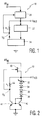
- a temperature-compensated voltage regulator 10 is shown in partly-schematic and partly-block diagram form in Fig. 1.
- the voltage regulator 10 includes a voltage buffer 20 having a high-voltage input HV IN , a control input V G and a low-voltage output V REG .
- a voltage generator 22 for generating a reference voltage is coupled between the low-voltage output of the voltage buffer and an input of a current mirror 24.
- the current mirror also has a common terminal, typically ground, and an output which is coupled to the control input V G of the voltage buffer 20.
- the configuration of Fig. 1 is completed by a resistor R L which couples the output of the current mirror 24 to the low-voltage output V REG , with the regulated output voltage being generated between the low-voltage output V REG of the voltage buffer and the common (ground) terminal.
- the voltage buffer of the voltage regulator 10 is formed by a junction field effect transistor (JFET) 30 having its main current path connected between the high-voltage input HV IN and the low-voltage output V REG .
- the voltage generator includes a series connection of a zener diode 32 and at least one (here three) p-n junction diodes 34, 36 and 38.
- Diode 38 is coupled to the current mirror by being connected to the collector and base of diode-connected transistor 40, whose emitter is connected to ground, and the output of the current mirror, at the collector of a transistor 42, is connected to the gate of buffer transistor 30 (V G ).
- the base of transistor 42 is connected to the base of transistor 40, and the emitter of transmitter 42 is connected to ground.
- the circuit configuration is completed by coupling the collector of transistor 42 and the gate of transistor 30 (V G ) through load resistor 44 (R L ) to the low- voltage output V REG .
- resistor R L is not critical, it will typically will have a high resistance value, such as 100K ohms, in order to minimize power consumption.
- the magnitude of the regulated output voltage V REG is determined by appropriate selection of the zener voltage of zener diode 32, and by selection of the number of series-connected diodes coupled between zener diode 32 and transistor 40.
- zener diode 32 has a zener voltage of 9.5 volts, and three p-n diodes (34, 36 and 38) are connected between the zener diode and diode-connected transistor 40.
- the regulated output voltage V REG will be equal to 9.5 volts plus a total of four forward voltage drops of about 0.7 volts each (i.e.,the voltage drops across p-n diodes 34, 36 and 38, plus the voltage drop across diode-connected transistor 40) for a total regulated output voltage of about 12.3 volts.
- the temperature coefficient of the zener diode is about +8 mV/°C, while each p-n junction diode has a temperature coefficient of about - 2mV/°C.
- the effective temperature coefficient of the three p-n diodes plus the diode-connected transistor is therefore about -8mV/°C, thus to a first order essentially balancing the +8mV/°C temperature coeffecient of the zener diode and providing a net temperature coefficient of zero.
- zener diode voltage, temperature coefficients, and numbers of p-n junction diodes can be employed, consistent with the goals of providing a desired output voltage in combination with a zero first-order temperature coefficient.
- a high voltage input (up to about 500 volts depending upon the design of buffer transistor 30) is applied to the high-voltage input HV IN .
- Transistor 30 will then conduct, causing current to flow to ground through the series-connected diodes 32, 34, 36 and 38, and diode-connected transistor 40 of the current mirror. The voltage drops across these components will establish an output voltage at the low-voltage output V REG of about 12 volts with respect to ground.
- the current flowing into transistor 40 will be reflected by the current mirror to cause a proportional current flow through resistor 44 and transistor 42. This current flow through resistor 44 will establish a gate voltage V G at the gate of buffer transistor 30 which is equal to the regulated output voltage less the voltage drop caused by the current flowing through resistor 44.
- the circuit shown in Fig. 2 offers several important advantages over more complex prior-art circuits.
- the circuit is both self-starting and self-biasing, thus providing reliable performance, and is capable of handling input voltages as high as 500 volts with appropriate selection of buffer transistor 30.
- the disclosed circuit is capable of providing a desired regulated output voltage along with good temperature compensation.
- the circuit features low power consumption and, due to its simplicity, offers the additional advantages of stability, compactness and economy, and can be easily fabricated using conventional integrated circuit technology.
- buffer transistor 30 may be a depletion-mode MOSFET rather than a JFET, and MOS transistors, rather than bipolar transistors, may be used for transistors 40 and 42 of the current mirror.
- MOS transistors rather than bipolar transistors
- various types and numbers of series-connected diodes may be used in order to achieve a desired regulated output voltage and desired temperature compensation characteristics.
Landscapes
- Engineering & Computer Science (AREA)
- Physics & Mathematics (AREA)
- Microelectronics & Electronic Packaging (AREA)
- Nonlinear Science (AREA)
- Electromagnetism (AREA)
- General Physics & Mathematics (AREA)
- Radar, Positioning & Navigation (AREA)
- Automation & Control Theory (AREA)
- Control Of Electrical Variables (AREA)
Applications Claiming Priority (2)
| Application Number | Priority Date | Filing Date | Title |
|---|---|---|---|
| US08/043,418 US5519313A (en) | 1993-04-06 | 1993-04-06 | Temperature-compensated voltage regulator |
| US43418 | 1993-04-06 |
Publications (3)
| Publication Number | Publication Date |
|---|---|
| EP0620514A2 true EP0620514A2 (de) | 1994-10-19 |
| EP0620514A3 EP0620514A3 (de) | 1995-08-09 |
| EP0620514B1 EP0620514B1 (de) | 2000-03-01 |
Family
ID=21927083
Family Applications (1)
| Application Number | Title | Priority Date | Filing Date |
|---|---|---|---|
| EP94200862A Expired - Lifetime EP0620514B1 (de) | 1993-04-06 | 1994-03-30 | Temperaturkompensierter Spannungsregler |
Country Status (4)
| Country | Link |
|---|---|
| US (1) | US5519313A (de) |
| EP (1) | EP0620514B1 (de) |
| JP (1) | JPH06309049A (de) |
| DE (1) | DE69423121T2 (de) |
Cited By (3)
| Publication number | Priority date | Publication date | Assignee | Title |
|---|---|---|---|---|
| EP1253498A1 (de) * | 2001-04-24 | 2002-10-30 | Infineon Technologies AG | Spannungsregler |
| WO2012003871A1 (en) * | 2010-07-07 | 2012-01-12 | Epcos Ag | Voltage regulator and a method for reducing an influence of a threshold voltage variation |
| CN105388950A (zh) * | 2015-12-21 | 2016-03-09 | 哈尔滨工业大学 | 基于电流镜的耐高温恒流启动电路 |
Families Citing this family (17)
| Publication number | Priority date | Publication date | Assignee | Title |
|---|---|---|---|---|
| JP2000277622A (ja) * | 1999-01-18 | 2000-10-06 | Sony Corp | 半導体装置およびその製造方法 |
| US6222350B1 (en) * | 2000-01-21 | 2001-04-24 | Titan Specialties, Ltd. | High temperature voltage regulator circuit |
| DE10146849A1 (de) * | 2001-09-24 | 2003-04-10 | Atmel Germany Gmbh | Verfahren zur Erzeugung einer Ausgangsspannung |
| US6885239B2 (en) * | 2001-10-31 | 2005-04-26 | Kabushiki Kaisha Toshiba | Mobility proportion current generator, and bias generator and amplifier using the same |
| US7554314B2 (en) * | 2005-11-04 | 2009-06-30 | Denso Corporation | Current mirror circuit for reducing chip size |
| US8552698B2 (en) * | 2007-03-02 | 2013-10-08 | International Rectifier Corporation | High voltage shunt-regulator circuit with voltage-dependent resistor |
| US8203276B2 (en) * | 2008-11-28 | 2012-06-19 | Lightech Electronic Industries Ltd. | Phase controlled dimming LED driver system and method thereof |
| US9167641B2 (en) * | 2008-11-28 | 2015-10-20 | Lightech Electronic Industries Ltd. | Phase controlled dimming LED driver system and method thereof |
| US20100194465A1 (en) * | 2009-02-02 | 2010-08-05 | Ali Salih | Temperature compensated current source and method therefor |
| US8169844B2 (en) * | 2009-06-30 | 2012-05-01 | Agere Systems Inc. | Memory built-in self-characterization |
| JP5581868B2 (ja) * | 2010-07-15 | 2014-09-03 | 株式会社リコー | 半導体回路及びそれを用いた定電圧回路 |
| JP5392225B2 (ja) * | 2010-10-07 | 2014-01-22 | 株式会社デンソー | 半導体装置、及び、その製造方法 |
| JP6061033B2 (ja) * | 2013-06-20 | 2017-01-18 | 富士電機株式会社 | 基準電圧回路 |
| US9602100B1 (en) * | 2014-01-22 | 2017-03-21 | Automation Solutions, LLC | Downhole measurement tool having a regulated voltage power supply and method of use thereof |
| CN103956906B (zh) * | 2014-04-21 | 2016-07-27 | 华为技术有限公司 | 一种反馈控制电路 |
| US20180173259A1 (en) * | 2016-12-20 | 2018-06-21 | Silicon Laboratories Inc. | Apparatus for Regulator with Improved Performance and Associated Methods |
| WO2022030119A1 (ja) * | 2020-08-06 | 2022-02-10 | 富士電機株式会社 | 電源回路、スイッチング制御回路 |
Family Cites Families (16)
| Publication number | Priority date | Publication date | Assignee | Title |
|---|---|---|---|---|
| DE2237559C3 (de) * | 1972-07-31 | 1975-05-28 | Deutsche Itt Industries Gmbh, 7800 Freiburg | Monolithisch integrierte Schaltungsanordnung zur Spannungsstabilisierung |
| DE2314423C3 (de) * | 1973-03-23 | 1981-08-27 | Robert Bosch Gmbh, 7000 Stuttgart | Verfahren zur Herstellung einer Referenzgleichspannungsquelle |
| US4030023A (en) * | 1976-05-25 | 1977-06-14 | Rockwell International Corporation | Temperature compensated constant voltage apparatus |
| GB2146808B (en) * | 1983-09-15 | 1986-11-12 | Ferranti Plc | Constant voltage circuits |
| IT1179823B (it) * | 1984-11-22 | 1987-09-16 | Cselt Centro Studi Lab Telecom | Generatore di tensione differenziale di rifferimento per circuiti integrati ad alimentazione singola in tecnologia nmos |
| KR910001293B1 (ko) * | 1986-03-31 | 1991-02-28 | 가부시키가이샤 도시바 | 전원전압검출회로 |
| US4686451A (en) * | 1986-10-15 | 1987-08-11 | Triquint Semiconductor, Inc. | GaAs voltage reference generator |
| US4774452A (en) * | 1987-05-29 | 1988-09-27 | Ge Company | Zener referenced voltage circuit |
| US4890052A (en) * | 1988-08-04 | 1989-12-26 | Texas Instruments Incorporated | Temperature constant current reference |
| US5023543A (en) * | 1989-09-15 | 1991-06-11 | Gennum Corporation | Temperature compensated voltage regulator and reference circuit |
| NL9001018A (nl) * | 1990-04-27 | 1991-11-18 | Philips Nv | Referentiegenerator. |
| US5084665A (en) * | 1990-06-04 | 1992-01-28 | Motorola, Inc. | Voltage reference circuit with power supply compensation |
| US5334929A (en) * | 1992-08-26 | 1994-08-02 | Harris Corporation | Circuit for providing a current proportional to absolute temperature |
| US5352973A (en) * | 1993-01-13 | 1994-10-04 | Analog Devices, Inc. | Temperature compensation bandgap voltage reference and method |
| US5430367A (en) * | 1993-01-19 | 1995-07-04 | Delco Electronics Corporation | Self-regulating band-gap voltage regulator |
| US5402061A (en) * | 1993-08-13 | 1995-03-28 | Tektronix, Inc. | Temperature independent current source |
-
1993
- 1993-04-06 US US08/043,418 patent/US5519313A/en not_active Expired - Fee Related
-
1994
- 1994-03-30 DE DE69423121T patent/DE69423121T2/de not_active Expired - Fee Related
- 1994-03-30 EP EP94200862A patent/EP0620514B1/de not_active Expired - Lifetime
- 1994-04-04 JP JP6066027A patent/JPH06309049A/ja active Pending
Cited By (6)
| Publication number | Priority date | Publication date | Assignee | Title |
|---|---|---|---|---|
| EP1253498A1 (de) * | 2001-04-24 | 2002-10-30 | Infineon Technologies AG | Spannungsregler |
| US6700361B2 (en) | 2001-04-24 | 2004-03-02 | Infineon Technologies Ag | Voltage regulator with a stabilization circuit for guaranteeing stabile operation |
| WO2012003871A1 (en) * | 2010-07-07 | 2012-01-12 | Epcos Ag | Voltage regulator and a method for reducing an influence of a threshold voltage variation |
| US9280169B2 (en) | 2010-07-07 | 2016-03-08 | Epcos Ag | Voltage regulator and a method for reducing an influence of a threshold voltage variation |
| CN105388950A (zh) * | 2015-12-21 | 2016-03-09 | 哈尔滨工业大学 | 基于电流镜的耐高温恒流启动电路 |
| CN105388950B (zh) * | 2015-12-21 | 2016-11-23 | 哈尔滨工业大学 | 基于电流镜的耐高温恒流启动电路 |
Also Published As
| Publication number | Publication date |
|---|---|
| DE69423121T2 (de) | 2000-09-21 |
| EP0620514A3 (de) | 1995-08-09 |
| US5519313A (en) | 1996-05-21 |
| DE69423121D1 (de) | 2000-04-06 |
| JPH06309049A (ja) | 1994-11-04 |
| EP0620514B1 (de) | 2000-03-01 |
Similar Documents
| Publication | Publication Date | Title |
|---|---|---|
| EP0620514B1 (de) | Temperaturkompensierter Spannungsregler | |
| US4352056A (en) | Solid-state voltage reference providing a regulated voltage having a high magnitude | |
| EP1557679B1 (de) | Hochspannungsstromdetektor | |
| US5404053A (en) | Circuit for controlling the maximum current in a MOS power transistor used for driving a load connected to earth | |
| US4902959A (en) | Band-gap voltage reference with independently trimmable TC and output | |
| US4528496A (en) | Current supply for use in low voltage IC devices | |
| US6124704A (en) | Reference voltage source with temperature-compensated output reference voltage | |
| EP0155720B1 (de) | Kaskadenstromquellenanordnung | |
| US4563632A (en) | Monolithically integratable constant-current generating circuit with low supply voltage | |
| US4339677A (en) | Electrically variable impedance circuit with feedback compensation | |
| US4091321A (en) | Low voltage reference | |
| US5051686A (en) | Bandgap voltage reference | |
| US4268789A (en) | Limiter circuit | |
| US5015942A (en) | Positive temperature coefficient current source with low power dissipation | |
| US6380723B1 (en) | Method and system for generating a low voltage reference | |
| EP0181017B1 (de) | Transistor oder Diode simulierende Schaltungsanordnung | |
| US5283537A (en) | Current mirror circuit | |
| US6570437B2 (en) | Bandgap reference voltage circuit | |
| US4335346A (en) | Temperature independent voltage supply | |
| US6144250A (en) | Error amplifier reference circuit | |
| US4644249A (en) | Compensated bias generator voltage source for ECL circuits | |
| US4433283A (en) | Band gap regulator circuit | |
| US4571536A (en) | Semiconductor voltage supply circuit having constant output voltage characteristic | |
| US6605987B2 (en) | Circuit for generating a reference voltage based on two partial currents with opposite temperature dependence | |
| JPH0795249B2 (ja) | 定電圧装置 |
Legal Events
| Date | Code | Title | Description |
|---|---|---|---|
| PUAI | Public reference made under article 153(3) epc to a published international application that has entered the european phase |
Free format text: ORIGINAL CODE: 0009012 |
|
| AK | Designated contracting states |
Kind code of ref document: A2 Designated state(s): DE FR GB IT NL |
|
| PUAL | Search report despatched |
Free format text: ORIGINAL CODE: 0009013 |
|
| AK | Designated contracting states |
Kind code of ref document: A3 Designated state(s): DE FR GB IT NL |
|
| 17P | Request for examination filed |
Effective date: 19960209 |
|
| RAP3 | Party data changed (applicant data changed or rights of an application transferred) |
Owner name: KONINKLIJKE PHILIPS ELECTRONICS N.V. |
|
| GRAG | Despatch of communication of intention to grant |
Free format text: ORIGINAL CODE: EPIDOS AGRA |
|
| 17Q | First examination report despatched |
Effective date: 19990521 |
|
| GRAG | Despatch of communication of intention to grant |
Free format text: ORIGINAL CODE: EPIDOS AGRA |
|
| GRAH | Despatch of communication of intention to grant a patent |
Free format text: ORIGINAL CODE: EPIDOS IGRA |
|
| GRAH | Despatch of communication of intention to grant a patent |
Free format text: ORIGINAL CODE: EPIDOS IGRA |
|
| GRAA | (expected) grant |
Free format text: ORIGINAL CODE: 0009210 |
|
| AK | Designated contracting states |
Kind code of ref document: B1 Designated state(s): DE FR GB IT NL |
|
| PG25 | Lapsed in a contracting state [announced via postgrant information from national office to epo] |
Ref country code: NL Free format text: LAPSE BECAUSE OF FAILURE TO SUBMIT A TRANSLATION OF THE DESCRIPTION OR TO PAY THE FEE WITHIN THE PRESCRIBED TIME-LIMIT Effective date: 20000301 Ref country code: IT Free format text: LAPSE BECAUSE OF FAILURE TO SUBMIT A TRANSLATION OF THE DESCRIPTION OR TO PAY THE FEE WITHIN THE PRESCRIBED TIME-LIMIT;WARNING: LAPSES OF ITALIAN PATENTS WITH EFFECTIVE DATE BEFORE 2007 MAY HAVE OCCURRED AT ANY TIME BEFORE 2007. THE CORRECT EFFECTIVE DATE MAY BE DIFFERENT FROM THE ONE RECORDED. Effective date: 20000301 |
|
| REF | Corresponds to: |
Ref document number: 69423121 Country of ref document: DE Date of ref document: 20000406 |
|
| ET | Fr: translation filed | ||
| NLV1 | Nl: lapsed or annulled due to failure to fulfill the requirements of art. 29p and 29m of the patents act | ||
| PLBE | No opposition filed within time limit |
Free format text: ORIGINAL CODE: 0009261 |
|
| STAA | Information on the status of an ep patent application or granted ep patent |
Free format text: STATUS: NO OPPOSITION FILED WITHIN TIME LIMIT |
|
| 26N | No opposition filed | ||
| PGFP | Annual fee paid to national office [announced via postgrant information from national office to epo] |
Ref country code: FR Payment date: 20010326 Year of fee payment: 8 |
|
| PGFP | Annual fee paid to national office [announced via postgrant information from national office to epo] |
Ref country code: GB Payment date: 20010330 Year of fee payment: 8 |
|
| PGFP | Annual fee paid to national office [announced via postgrant information from national office to epo] |
Ref country code: DE Payment date: 20010516 Year of fee payment: 8 |
|
| REG | Reference to a national code |
Ref country code: GB Ref legal event code: IF02 |
|
| PG25 | Lapsed in a contracting state [announced via postgrant information from national office to epo] |
Ref country code: GB Free format text: LAPSE BECAUSE OF NON-PAYMENT OF DUE FEES Effective date: 20020330 |
|
| PG25 | Lapsed in a contracting state [announced via postgrant information from national office to epo] |
Ref country code: DE Free format text: LAPSE BECAUSE OF NON-PAYMENT OF DUE FEES Effective date: 20021001 |
|
| GBPC | Gb: european patent ceased through non-payment of renewal fee |
Effective date: 20020330 |
|
| PG25 | Lapsed in a contracting state [announced via postgrant information from national office to epo] |
Ref country code: FR Free format text: LAPSE BECAUSE OF NON-PAYMENT OF DUE FEES Effective date: 20021129 |
|
| REG | Reference to a national code |
Ref country code: FR Ref legal event code: ST |