EP0620636B1 - Oszillator mit einer spannungsgesteuerten Frequenz - Google Patents
Oszillator mit einer spannungsgesteuerten Frequenz Download PDFInfo
- Publication number
- EP0620636B1 EP0620636B1 EP94200944A EP94200944A EP0620636B1 EP 0620636 B1 EP0620636 B1 EP 0620636B1 EP 94200944 A EP94200944 A EP 94200944A EP 94200944 A EP94200944 A EP 94200944A EP 0620636 B1 EP0620636 B1 EP 0620636B1
- Authority
- EP
- European Patent Office
- Prior art keywords
- oscillator
- electrode
- inductance
- series
- parallel
- Prior art date
- Legal status (The legal status is an assumption and is not a legal conclusion. Google has not performed a legal analysis and makes no representation as to the accuracy of the status listed.)
- Expired - Lifetime
Links
- 230000008878 coupling Effects 0.000 claims description 4
- 238000010168 coupling process Methods 0.000 claims description 4
- 238000005859 coupling reaction Methods 0.000 claims description 4
- 239000003990 capacitor Substances 0.000 description 17
- 230000010355 oscillation Effects 0.000 description 13
- 230000003071 parasitic effect Effects 0.000 description 6
- 230000000903 blocking effect Effects 0.000 description 4
- 238000010586 diagram Methods 0.000 description 4
- 230000000694 effects Effects 0.000 description 4
- 238000002955 isolation Methods 0.000 description 2
- 230000002301 combined effect Effects 0.000 description 1
- 238000010276 construction Methods 0.000 description 1
- 230000007423 decrease Effects 0.000 description 1
- 230000002349 favourable effect Effects 0.000 description 1
- 230000005669 field effect Effects 0.000 description 1
- 230000037431 insertion Effects 0.000 description 1
- 238000003780 insertion Methods 0.000 description 1
- 238000009413 insulation Methods 0.000 description 1
- 244000045947 parasite Species 0.000 description 1
Images
Classifications
-
- H—ELECTRICITY
- H03—ELECTRONIC CIRCUITRY
- H03B—GENERATION OF OSCILLATIONS, DIRECTLY OR BY FREQUENCY-CHANGING, BY CIRCUITS EMPLOYING ACTIVE ELEMENTS WHICH OPERATE IN A NON-SWITCHING MANNER; GENERATION OF NOISE BY SUCH CIRCUITS
- H03B5/00—Generation of oscillations using amplifier with regenerative feedback from output to input
- H03B5/08—Generation of oscillations using amplifier with regenerative feedback from output to input with frequency-determining element comprising lumped inductance and capacitance
- H03B5/12—Generation of oscillations using amplifier with regenerative feedback from output to input with frequency-determining element comprising lumped inductance and capacitance active element in amplifier being semiconductor device
- H03B5/1231—Generation of oscillations using amplifier with regenerative feedback from output to input with frequency-determining element comprising lumped inductance and capacitance active element in amplifier being semiconductor device the amplifier comprising one or more bipolar transistors
-
- H—ELECTRICITY
- H03—ELECTRONIC CIRCUITRY
- H03B—GENERATION OF OSCILLATIONS, DIRECTLY OR BY FREQUENCY-CHANGING, BY CIRCUITS EMPLOYING ACTIVE ELEMENTS WHICH OPERATE IN A NON-SWITCHING MANNER; GENERATION OF NOISE BY SUCH CIRCUITS
- H03B5/00—Generation of oscillations using amplifier with regenerative feedback from output to input
- H03B5/08—Generation of oscillations using amplifier with regenerative feedback from output to input with frequency-determining element comprising lumped inductance and capacitance
- H03B5/12—Generation of oscillations using amplifier with regenerative feedback from output to input with frequency-determining element comprising lumped inductance and capacitance active element in amplifier being semiconductor device
- H03B5/1203—Generation of oscillations using amplifier with regenerative feedback from output to input with frequency-determining element comprising lumped inductance and capacitance active element in amplifier being semiconductor device the amplifier being a single transistor
-
- H—ELECTRICITY
- H03—ELECTRONIC CIRCUITRY
- H03B—GENERATION OF OSCILLATIONS, DIRECTLY OR BY FREQUENCY-CHANGING, BY CIRCUITS EMPLOYING ACTIVE ELEMENTS WHICH OPERATE IN A NON-SWITCHING MANNER; GENERATION OF NOISE BY SUCH CIRCUITS
- H03B5/00—Generation of oscillations using amplifier with regenerative feedback from output to input
- H03B5/08—Generation of oscillations using amplifier with regenerative feedback from output to input with frequency-determining element comprising lumped inductance and capacitance
- H03B5/12—Generation of oscillations using amplifier with regenerative feedback from output to input with frequency-determining element comprising lumped inductance and capacitance active element in amplifier being semiconductor device
- H03B5/1237—Generation of oscillations using amplifier with regenerative feedback from output to input with frequency-determining element comprising lumped inductance and capacitance active element in amplifier being semiconductor device comprising means for varying the frequency of the generator
- H03B5/124—Generation of oscillations using amplifier with regenerative feedback from output to input with frequency-determining element comprising lumped inductance and capacitance active element in amplifier being semiconductor device comprising means for varying the frequency of the generator the means comprising a voltage dependent capacitance
- H03B5/1243—Generation of oscillations using amplifier with regenerative feedback from output to input with frequency-determining element comprising lumped inductance and capacitance active element in amplifier being semiconductor device comprising means for varying the frequency of the generator the means comprising a voltage dependent capacitance the means comprising voltage variable capacitance diodes
-
- H—ELECTRICITY
- H03—ELECTRONIC CIRCUITRY
- H03B—GENERATION OF OSCILLATIONS, DIRECTLY OR BY FREQUENCY-CHANGING, BY CIRCUITS EMPLOYING ACTIVE ELEMENTS WHICH OPERATE IN A NON-SWITCHING MANNER; GENERATION OF NOISE BY SUCH CIRCUITS
- H03B2200/00—Indexing scheme relating to details of oscillators covered by H03B
- H03B2200/003—Circuit elements of oscillators
- H03B2200/004—Circuit elements of oscillators including a variable capacitance, e.g. a varicap, a varactor or a variable capacitance of a diode or transistor
-
- H—ELECTRICITY
- H03—ELECTRONIC CIRCUITRY
- H03B—GENERATION OF OSCILLATIONS, DIRECTLY OR BY FREQUENCY-CHANGING, BY CIRCUITS EMPLOYING ACTIVE ELEMENTS WHICH OPERATE IN A NON-SWITCHING MANNER; GENERATION OF NOISE BY SUCH CIRCUITS
- H03B2201/00—Aspects of oscillators relating to varying the frequency of the oscillations
- H03B2201/02—Varying the frequency of the oscillations by electronic means
- H03B2201/0208—Varying the frequency of the oscillations by electronic means the means being an element with a variable capacitance, e.g. capacitance diode
Definitions
- the present invention relates to a voltage-controlled frequency oscillator comprising on the one hand, an amplifier device which has a main current path defined between a first and a second electrode, and a control electrode for controlling the conduction of this device. , further comprising a capacitive divider bridge performing reactive coupling between the first electrode of the device and its control electrode, one end of the divider bridge being connected to the control electrode, the other end connected to a voltage reference and the intermediate node, connected to the first electrode, oscillator to which a tuning circuit is still connected, disposed between the control electrode and the voltage reference, which circuit comprises: a first parallel branch formed by an inductance of tuning in series with a first variable capacitance, and a second parallel branch equivalent alente to a second variable capacity.
- Such an oscillator of the Colpitts type, is known from document EP-A-0 270 298. It is in particular used as a local oscillator for the reception of television signals.
- a constant technical problem in this field lies in the ability to cover the widest possible frequency range, starting from a determined tuning inductance, while maintaining reliable conditions of oscillation of the amplifier device.
- the reactive impedance values are likely to vary in large proportions, from the lowest frequency to the highest frequency of the envisaged frequency range, it is most often necessary to use a tuning circuit having a relatively complex arrangement, achieving a satisfactory compromise between the operational safety of the oscillator, and the extent of the frequency range covered.
- the known oscillator recommends the use of a tuning circuit having said second parallel branch, in order to widen the range of frequencies covered by the variation in capacitance of varicap diodes which constitute said variable capacitors.
- a tuning circuit having said second parallel branch, in order to widen the range of frequencies covered by the variation in capacitance of varicap diodes which constitute said variable capacitors.
- the object of the invention is to provide an oscillator having a very wide frequency range, while ensuring reliable oscillation conditions for the amplifier device, throughout the entire range of the frequency range.
- an oscillator of the type defined in the introductory paragraph is notably remarkable in that the tuning circuit comprises a third parallel branch made up of a fixed capacitance, and in that all of the first and third parallel branches is connected to the connection node between the device control electrode and the second parallel branch via a series inductor whose value is less than that of the tuning inductor.
- all of the first and third parallel branches form a resonant circuit which can be described as a combination of a series mode and a parallel mode.
- the compromise is still too narrow between the width of the frequency band covered, and the stability of the oscillation at the band limit frequencies.
- the impedance of the tuning circuit decreases.
- the oscillation stops occurring because the tuning circuit dissipates more energy than the amplifying device can supply.
- the insertion of the series inductance introduces a possibility of resonance at a frequency other than that which is determined by the chord inductance and the series-parallel combination of the capacities provided in the tuning circuit.
- the value of the series inductance is chosen as being only a fraction of the value of the tuning inductance, so that the aforementioned undesirable frequency, is clearly higher than the frequency which is deduced from l inductance agree. It can be made so high that this parasitic oscillation, in reality, does not occur.
- the oscillator is characterized in that the second parallel branch consists of a fixed capacitance in series with a variable capacitance diode, of the same model as the diode with variable capacity constituting said first variable capacity.
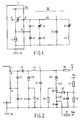
- the oscillator shown in FIG. 1, very schematically, comprises a portion of circuit 1, with negative resistance, in which a transistor T constitutes an amplifier device whose main current path is supplied between a supply voltage Vcc and a reference voltage VE. At the base of transistor T is connected a terminal A, and to the emitter of this transistor a terminal B. The emitter of transistor T is also connected to the reference voltage VE via a current source S.
- a current source S In the portion of circuit 1, only the transistor T and the current source S have been represented while other functionalities not shown may also be incorporated in the form of an integrated circuit monolithic, functionalities which do not directly concern the invention.
- the oscillation signal generated by transistor T can be taken from the base of this transistor, which is symbolically represented in the figure by the output terminal 0.
- a capacitive divider bridge provides reactive coupling between the emitter of transistor T and the base of this transistor, which divider bridge consists of capacitors 11 and 12 arranged in series, the free end of capacitor 11 connected to terminal A (base of transistor T) and the free end of capacitor 12 connected to the reference voltage VE.
- the common point between the capacitors 11 and 12 is connected to the terminal B (emitter of the transistor T).
- a tuning circuit 20 consisting of a first parallel branch formed of a tuning inductor La in series with a variable capacitance 21 and a second parallel branch formed by a second variable capacity 22 in series with a fixed capacity 23, this branch being equivalent to a variable capacity.
- a third branch in parallel on the first branch 21, La consists of a fixed capacitor 24.
- the first (21, La ) and third (24) parallel branches are joined in a node C.
- the divider bridge 11, 12 and the second parallel branch 22, 23 are directly connected to the terminal A.
- the node C is connected to terminal A via a series inductor Ls whose value is lower than that of the tuning inductor La .
- the Ls series inductor provides an effective means of ensuring that the oscillation conditions remain true at the highest frequencies when the range of frequencies over which the oscillator can be tuned has been extent.
- the presence of the series inductance Ls results in the fact that the tuning circuit 20 is capable of entering into resonance on two frequencies: one called the main one determined mainly by the tuning inductor La and the other called parasite determined by the Ls series inductance.
- the reactance with respect to the reference voltage VE is reduced to a capacitance resulting from the combination of the capacitors 11, 12, 23 and variable capacity 22.
- the parasitic resonance frequency can therefore be calculated and it will be determined mainly by the choice of the value of the capacitors 11, 12, 24 and of the inductance Ls .
- the inductance Ls has been chosen to be of low value in front of the tuning inductor La , it is easy to ensure that the parasitic resonant frequency is reported clearly beyond the highest frequency of the frequency range in the so-called main mode, so that the oscillation conditions on the parasitic frequency are not fulfilled.
- the conditions are more favorable since the parallel capacity equivalent to the series capacities 22 and 23, becomes low due to the variable capacity 22 when one places oneself at the high limit of the frequency range, and that it increases at the other end of the range, for the lowest frequencies.
- a widening of the frequency range is also obtained at high frequencies, which is however unimportant because the variable capacitance 22, although low, is located in parallel on the divider bridge 11, 12, which then has a preponderant influence.
- a significant increase in the tuning range requires increasing the equivalent parallel capacity at the lower limit of the frequency range. It is important, however, that the parallel capacitance has a high quality coefficient so as not to significantly lower the impedance of the tuning circuit at the lowest frequencies, which would make the operation of the oscillator at these frequencies critical. For this reason, increasing the equivalent parallel capacity obtained by simply increasing the value of capacity 23 is not a satisfactory solution.
- a higher quality coefficient is obtained if the equivalent parallel capacity is increased by means of an additional capacity (24) of fixed value, added in parallel to the branch of variable capacity. It follows a certain reduction in the impedance at high frequencies compared to the previous situation which is compensated in the present invention by the addition of the series inductor Ls.
- an extended frequency range is obtained by using two capacitive branches respectively 24 and 22, 23 in parallel on the first tuning branch La , 21, and by interposing the series inductance Ls between the node A and the node C.
- the level of impedance of the tuning circuit can be adapted almost optimally to that required to obtain correct operation of the oscillator over the frequency range sought.
- the choice of a capacitor 24 of relatively low value contributes to raising the level of impedance of the tuning circuit.
- the operation of the oscillator at these frequencies is also made easier by the presence of the inductance Ls . Detailed calculations show that this inductance has the effect of raising the impedance of the tuning circuit while having little effect on the oscillation frequency.
- variable capacitors 21 and 22 varying between 2.5 pF and 40 pF, it is found that in practice, it is possible to cover a range having an extreme frequency ratio which is as high as a factor 2.8, for a chord inductor La of given value.
- FIG. 2 An example of practical implementation of the invention is represented by the oscillator in FIG. 2.
- the elements corresponding to FIG. 1 and ensuring the same function are assigned the same reference signs.
- variable capacitors 22 respectively 21 of FIG. 1 are here produced by means of variable capacitance diodes C22 respectively C21, of the same model, both controlled from the same adjustment voltage VT which is applied to the node C via a blocking resistor 30 of high value.
- the DC isolation between node C and terminal A is ensured by means of a link capacity 32 of high value chosen so that its reactance is low throughout the frequency range.
- the anode of the diode C22 is brought to the direct potential of the reference voltage VE (ground) by means of a blocking resistor 34 while a similar arrangement is applied to the diode C21 whose anode, through the tuning inductor La 1, is brought to the DC reference potential VE via a blocking resistor 36.
- a blocking resistor 34 is applied to the diode C21 whose anode, through the tuning inductor La 1, is brought to the DC reference potential VE via a blocking resistor 36.
- an additional inductance La 2 whose value is higher than the inductance La 1, the sum of these inductances being used to cover the lowest range of the frequencies sought.
- isolation is carried out on either side of the additional inductance La2 by capacitors 38 and 40 of high values so that at the frequencies used the impedance of these capacitors is negligible.
- a band switching circuit is produced by means of a switching diode 42 whose anode is connected between the capacitance 38 and the inductance La2 and whose cathode is brought to a potential intermediate between the supply voltage Vcc and the reference voltage VE by means of a resistive bridge 44, 46. Finally, the anode of the switching diode 42 can be brought either a voltage equal to Vcc to place this diode in conduction, or to a voltage equal to the reference voltage VE to place this diode in blocking mode, this under the effect of a switching signal Vsw applied via an insulation resistance 48 to the node joining the capacitor 40 and the additional inductance La 2. When the diode 42 is conductive, it transmits the alternating signal at the reference voltage VE through a selected capacity 50 of a high value such that its impedance is negligible in alternating mode.
- the diagram in FIG. 2 conforms to the principle of the diagram in FIG. 1, in which the tuning inductor La can take two distinct values.
- the oscillator of FIG. 2 makes it possible in practice to cover the VHF television frequency band from 87 to 204 MHz as well as the VHF band from 188 to 513 MHz in a construction where the elements have the following values: Capacities References Values 11, 12 15 pF 23 47 pF 24 8 pF C21, C22 2.5 to 40 pF 32 100 pF 38, 40, 50 1nf Inductors La1 35 nH La2 160 nH Ls 7 nH Resistors 30, 34, 36 27 KOhms 48 390 Ohms 44 1 KOhms 46 680 Ohms Tensions Vcc 5 Volts VE 0 Vsw 0 or 5 Volts VT 0.5 to 28 Volts
- the invention is not limited to the use of a bipolar transistor as an amplifier device T, as described in the examples, but also applies to any other device, in particular field effect transistor, as soon as reactive coupling can be carried out between its control electrode (grid) and its first electrode (source), the main current path being defined between source and drain.
Landscapes
- Inductance-Capacitance Distribution Constants And Capacitance-Resistance Oscillators (AREA)
Claims (4)
- Die vorliegende Erfindung betrifft einen Oszillator mit einer spannungsgesteuerten Frequenz, bestehend einerseits aus einer Verstärkereinrichtung (T), die einen zwischen einer ersten und einer zweiten Elektrode definierten Hauptstromweg und eine Steuerelektrode für die Leitungssteuerung der Einrichtung aufweist, bestehend andererseits aus einer kapazitiven Teilerbrücke (11, 12), die eine reaktive Kopplung zwischen der ersten Elektrode der Einrichtung und ihrer Steuerelektrode vornimmt, wobei ein Ende der Teilerbrücke an die Steuerelektrode, das andere Ende an eine Spannungsreferenz (VE) und der Zwischenknoten an die erste Elektrode angeschlossen ist, während an den Oszillator zusätzlich zwischen der Steuerelektrode und der Spannungsreferenz ein Abstimmkreis (20) angeschlossen ist und die Schaltung folgendes enthält :
einen ersten aus einer Abstimminduktanz (La) in Serie mit einer ersten variablen Kapazität (21) gebildeten parallelen Zweig und einen zweiten, mit einer zweiten variablen Kapazität (22, 23) äquivalenten parallelen Zweig, mit dem Merkmal, daß die Abstimmschaltung einen dritten, aus einer festen Kapazität (24) gebildeten parallelen Zweig enthält und daß die Gesamtheit der ersten und dritten parallelen Zweige mit einem Verbindungsknoten (A) zwischen der Steuerelektrode der Einrichtung und dem zweiten parallelen Zweig verbunden ist, über eine Serieninduktanz (Ls), deren Wert unter dem der Abstimminduktanz (La) liegt. - Ein Oszillator laut Anspruch 1, mit dem Merkmal, daß der zweite parallele Zweig aus einer festen Kapazität (23) in Serie mit einer Diode variabler Kapazität (C22) gebildet wird, selben Modells wie die Diode variabler Kapazität (C21), die die besagte erste variable Kapazität bildet.
- Ein Oszillator laut Anspruch 2, mit dem Merkmal, daß die beiden Dioden variabler Kapazität (C21, C22) mit derselben variablen Steuerspannung (VT) gesteuert werden.
- Ein Oszillator laut einem beliebigen der Ansprüche 1 bis 3, mit dem Merkmal, daß die Verstärkereinrichtung (T) ein Bipolartransistor ist, dessen Basis die Steuerelektrode bildet, während der Emitter die besagte erste Elektrode und der Kollektor die besagte zweite Elektrode bildet.
Applications Claiming Priority (2)
| Application Number | Priority Date | Filing Date | Title |
|---|---|---|---|
| FR9304380A FR2704109A1 (fr) | 1993-04-14 | 1993-04-14 | Oscillateur à fréquence commandée par tension. |
| FR9304380 | 1993-04-14 |
Publications (2)
| Publication Number | Publication Date |
|---|---|
| EP0620636A1 EP0620636A1 (de) | 1994-10-19 |
| EP0620636B1 true EP0620636B1 (de) | 1997-10-15 |
Family
ID=9446051
Family Applications (1)
| Application Number | Title | Priority Date | Filing Date |
|---|---|---|---|
| EP94200944A Expired - Lifetime EP0620636B1 (de) | 1993-04-14 | 1994-04-07 | Oszillator mit einer spannungsgesteuerten Frequenz |
Country Status (5)
| Country | Link |
|---|---|
| US (1) | US5469117A (de) |
| EP (1) | EP0620636B1 (de) |
| JP (1) | JPH0746038A (de) |
| DE (1) | DE69406177T2 (de) |
| FR (1) | FR2704109A1 (de) |
Families Citing this family (8)
| Publication number | Priority date | Publication date | Assignee | Title |
|---|---|---|---|---|
| US5583759A (en) * | 1993-11-22 | 1996-12-10 | Huntington Bancshares, Inc. | Mechanism for expediting the deposit, transport and submission of checks into the payment system |
| US5892410A (en) * | 1997-02-19 | 1999-04-06 | Motorola, Inc. | Method and apparatus for transmitting radio frequency signals |
| WO2000003488A2 (en) * | 1998-07-13 | 2000-01-20 | Safety 1St, Inc. | Device for transmitting and receiving audible signals |
| US6431000B1 (en) * | 2000-05-23 | 2002-08-13 | General Electric Company | Method and apparatus for high cycle fatigue life test |
| US6509799B1 (en) * | 2000-11-09 | 2003-01-21 | Intel Corporation | Electrically tuned integrated amplifier for wireless communications |
| US6466099B2 (en) * | 2001-01-03 | 2002-10-15 | Motorola, Inc. | Voltage controlled oscillator (VCO) in colpitts configuration |
| GB2401263B (en) * | 2003-04-29 | 2006-01-11 | Motorola Inc | Wireless communication terminal and voltage controlled oscillator therefor |
| CN106877819B (zh) | 2016-11-21 | 2020-08-11 | 成都仕芯半导体有限公司 | 基于复合型谐振器的压控振荡器 |
Family Cites Families (10)
| Publication number | Priority date | Publication date | Assignee | Title |
|---|---|---|---|---|
| JPS4934262A (de) * | 1972-07-28 | 1974-03-29 | ||
| US3825858A (en) * | 1973-02-23 | 1974-07-23 | Hitachi Ltd | Local oscillator for use in a vhf tuner for a television receiver |
| US4074209A (en) * | 1976-12-13 | 1978-02-14 | Rca Corporation | Wide range frequency modulation of narrow loop bandwidth phase-locked oscillators |
| JPS58107703A (ja) * | 1981-12-21 | 1983-06-27 | Matsushita Electric Ind Co Ltd | 電圧制御発振器 |
| JPS58200606A (ja) * | 1982-05-17 | 1983-11-22 | Sharp Corp | 発振回路 |
| DE3246295C2 (de) * | 1982-12-14 | 1986-11-27 | Siemens AG, 1000 Berlin und 8000 München | Frequenzmodulierbarer Oszillator |
| DE3316881C1 (de) * | 1983-05-07 | 1990-01-25 | Deutsche Thomson-Brandt Gmbh, 7730 Villingen-Schwenningen | Oszillatorschaltung fuer Fernsehempfangsgeraete |
| US4593257A (en) * | 1985-02-28 | 1986-06-03 | Rca Corporation | Multiband local oscillator |
| US4736169A (en) * | 1986-09-29 | 1988-04-05 | Hughes Aircraft Company | Voltage controlled oscillator with frequency sensitivity control |
| US4743866A (en) * | 1986-11-26 | 1988-05-10 | Rca Corporation | Wide range oscillator |
-
1993
- 1993-04-14 FR FR9304380A patent/FR2704109A1/fr not_active Withdrawn
-
1994
- 1994-04-05 US US08/223,471 patent/US5469117A/en not_active Expired - Fee Related
- 1994-04-07 DE DE69406177T patent/DE69406177T2/de not_active Expired - Fee Related
- 1994-04-07 EP EP94200944A patent/EP0620636B1/de not_active Expired - Lifetime
- 1994-04-12 JP JP6073102A patent/JPH0746038A/ja active Pending
Also Published As
| Publication number | Publication date |
|---|---|
| FR2704109A1 (fr) | 1994-10-21 |
| DE69406177T2 (de) | 1998-03-26 |
| US5469117A (en) | 1995-11-21 |
| JPH0746038A (ja) | 1995-02-14 |
| DE69406177D1 (de) | 1997-11-20 |
| EP0620636A1 (de) | 1994-10-19 |
Similar Documents
| Publication | Publication Date | Title |
|---|---|---|
| EP0321329B1 (de) | Mittels Varaktoren abgestimmter Oszillator-Frequenzverdoppler | |
| FR2511821A1 (fr) | Dispositif d'accord de recepteur de television | |
| FR2602380A1 (fr) | Circuit gyrateur simulant une inductance | |
| FR2578124A1 (fr) | Circuit d'accord pour un tuner a plusieurs bandes | |
| FR2651075A1 (fr) | Correcteur de gain a pente variable en circuit integre monolithique a hyperfrequences | |
| EP0620636A1 (de) | Oszillator mit einer spannungsgesteuerten Frequenz | |
| FR2578123A1 (fr) | Reseau d'accouplement entre etages a bande changee comprenant un condensateur couple cote haut | |
| EP2202838B1 (de) | Kompakt geschalteter MEMS-Kondensator | |
| WO2002045263A1 (fr) | Filtre passe-bas ou passe-bande integre | |
| FR2644647A1 (fr) | Oscillateur hyperfrequence commande en tension | |
| EP0726648B1 (de) | Abstimmschaltung für Empfangsgerät insbesondere Fernsehempfänger | |
| CA2027885C (fr) | Cellule de filtrage et filtre correspondant | |
| FR2530907A1 (fr) | Dispositif de reglage d'accord pour recepteur de television a plusieurs bandes | |
| EP0201964B1 (de) | Verstärker für Hochfrequenzen | |
| FR2509928A1 (fr) | Reseau de transformation d'impedance pour filtre d'ondes acoustiques de surface | |
| FR2678450A1 (fr) | Dispositif de filtrage coupe-bande hyperfrequence. | |
| EP0120756B1 (de) | Hochfrequenzbandpassverstärker mit einem eine anpassbare Impedanz enthaltenden Oszillator | |
| FR2578375A1 (fr) | Agencement suiveur de la tension d'accord | |
| FR2588144A1 (fr) | Appareil commutateur de signaux haute frequence. | |
| EP0772359B1 (de) | Filtervorrichtung zur Verarbeitung einer Vielzahl von Kanälen in einem Kabelfernsehverteilungssystem | |
| FR2555847A1 (fr) | Filtre de preselection de canaux, notamment pour recepteur de television operant dans une bande etendue de frequences | |
| FR2612023A1 (fr) | Dispositif de commande bidirectionnelle d'un signal electrique de puissance a tres haute frequence | |
| EP0337825B1 (de) | Mikrowellensperrfilter in Mikrostreifenausführung | |
| EP0267100B1 (de) | Spannungsgesteuerter Mikrowellentransistoroszillator und solche Oszillatoren enthaltender breitbandiger Mikrowellengenerator | |
| FR2622067A1 (fr) | Amplificateur haute frequence avec circuit de neutrodynage automatique |
Legal Events
| Date | Code | Title | Description |
|---|---|---|---|
| PUAI | Public reference made under article 153(3) epc to a published international application that has entered the european phase |
Free format text: ORIGINAL CODE: 0009012 |
|
| AK | Designated contracting states |
Kind code of ref document: A1 Designated state(s): DE FR GB |
|
| 17P | Request for examination filed |
Effective date: 19950419 |
|
| RAP1 | Party data changed (applicant data changed or rights of an application transferred) |
Owner name: PHILIPS ELECTRONICS N.V. Owner name: PHILIPS COMPOSANTS ET SEMICONDUCTEURS |
|
| GRAG | Despatch of communication of intention to grant |
Free format text: ORIGINAL CODE: EPIDOS AGRA |
|
| 17Q | First examination report despatched |
Effective date: 19961218 |
|
| GRAH | Despatch of communication of intention to grant a patent |
Free format text: ORIGINAL CODE: EPIDOS IGRA |
|
| GRAH | Despatch of communication of intention to grant a patent |
Free format text: ORIGINAL CODE: EPIDOS IGRA |
|
| GRAA | (expected) grant |
Free format text: ORIGINAL CODE: 0009210 |
|
| AK | Designated contracting states |
Kind code of ref document: B1 Designated state(s): DE FR GB |
|
| REF | Corresponds to: |
Ref document number: 69406177 Country of ref document: DE Date of ref document: 19971120 |
|
| GBT | Gb: translation of ep patent filed (gb section 77(6)(a)/1977) |
Effective date: 19971110 |
|
| PLBE | No opposition filed within time limit |
Free format text: ORIGINAL CODE: 0009261 |
|
| STAA | Information on the status of an ep patent application or granted ep patent |
Free format text: STATUS: NO OPPOSITION FILED WITHIN TIME LIMIT |
|
| 26N | No opposition filed | ||
| REG | Reference to a national code |
Ref country code: FR Ref legal event code: TP |
|
| PGFP | Annual fee paid to national office [announced via postgrant information from national office to epo] |
Ref country code: FR Payment date: 20010423 Year of fee payment: 8 |
|
| PGFP | Annual fee paid to national office [announced via postgrant information from national office to epo] |
Ref country code: GB Payment date: 20010430 Year of fee payment: 8 |
|
| PGFP | Annual fee paid to national office [announced via postgrant information from national office to epo] |
Ref country code: DE Payment date: 20010620 Year of fee payment: 8 |
|
| REG | Reference to a national code |
Ref country code: GB Ref legal event code: IF02 |
|
| PG25 | Lapsed in a contracting state [announced via postgrant information from national office to epo] |
Ref country code: GB Free format text: LAPSE BECAUSE OF NON-PAYMENT OF DUE FEES Effective date: 20020407 |
|
| PG25 | Lapsed in a contracting state [announced via postgrant information from national office to epo] |
Ref country code: DE Free format text: LAPSE BECAUSE OF NON-PAYMENT OF DUE FEES Effective date: 20021101 |
|
| GBPC | Gb: european patent ceased through non-payment of renewal fee |
Effective date: 20020407 |
|
| PG25 | Lapsed in a contracting state [announced via postgrant information from national office to epo] |
Ref country code: FR Free format text: LAPSE BECAUSE OF NON-PAYMENT OF DUE FEES Effective date: 20021231 |
|
| REG | Reference to a national code |
Ref country code: FR Ref legal event code: ST |