EP0620662A1 - Dispositif de traitement, de sérialisation et de synchronisation - Google Patents
Dispositif de traitement, de sérialisation et de synchronisation Download PDFInfo
- Publication number
- EP0620662A1 EP0620662A1 EP93200442A EP93200442A EP0620662A1 EP 0620662 A1 EP0620662 A1 EP 0620662A1 EP 93200442 A EP93200442 A EP 93200442A EP 93200442 A EP93200442 A EP 93200442A EP 0620662 A1 EP0620662 A1 EP 0620662A1
- Authority
- EP
- European Patent Office
- Prior art keywords
- circuit
- serializing
- reset
- signal
- clock signal
- Prior art date
- Legal status (The legal status is an assumption and is not a legal conclusion. Google has not performed a legal analysis and makes no representation as to the accuracy of the status listed.)
- Ceased
Links
- 230000001360 synchronised effect Effects 0.000 claims abstract description 12
- 230000007704 transition Effects 0.000 claims abstract description 10
- 230000010363 phase shift Effects 0.000 claims abstract description 8
- 238000000034 method Methods 0.000 claims abstract description 4
- 230000003111 delayed effect Effects 0.000 claims description 14
- 238000001514 detection method Methods 0.000 claims description 9
- 102100040858 Dual specificity protein kinase CLK4 Human genes 0.000 description 23
- 101000749298 Homo sapiens Dual specificity protein kinase CLK4 Proteins 0.000 description 23
- 230000001934 delay Effects 0.000 description 6
- 238000005070 sampling Methods 0.000 description 6
- 238000010586 diagram Methods 0.000 description 4
- 125000004122 cyclic group Chemical group 0.000 description 1
- 230000001960 triggered effect Effects 0.000 description 1
Images




Classifications
-
- H—ELECTRICITY
- H03—ELECTRONIC CIRCUITRY
- H03L—AUTOMATIC CONTROL, STARTING, SYNCHRONISATION OR STABILISATION OF GENERATORS OF ELECTRONIC OSCILLATIONS OR PULSES
- H03L7/00—Automatic control of frequency or phase; Synchronisation
-
- H—ELECTRICITY
- H04—ELECTRIC COMMUNICATION TECHNIQUE
- H04J—MULTIPLEX COMMUNICATION
- H04J3/00—Time-division multiplex systems
- H04J3/02—Details
- H04J3/04—Distributors combined with modulators or demodulators
- H04J3/047—Distributors with transistors or integrated circuits
Definitions
- the present invention relates to a processing, serializing and synchronizing device including a processing means able to process a plurality of digital signals under control of a first clock signal and to be reset by a first reset signal, a serializing and synchronizing circuit able to be reset by a second reset signal and including a multiplexing device to convert the thus processed plurality of digital signals to a serialized output signal synchronous with a second clock signal, and a control circuit generating said first and second clock signals.
- Such a device is for instance used in a telecommunication system to process an incoming data stream at a lower rate than its input rate and to derive from the thus processed stream an output data stream at an output rate equal or even higher than the input rate.
- the processing means for instance demultiplexes the incoming data stream to provide the plurality of digital signals which can then be processed at a lower rate than the input rate, i.e. at the rate of the first clock signal, and the serializing and synchronizing circuit multiplexes the processed digital signals at the rate of the second clock signal which is at least equal to the input rate.
- the serializing and synchronizing circuit When the first reset signal is independent from the the second one and from the clock signals and when the serializing and synchronizing circuit operates without knowledge of the phase relationship between both the clock signals, it may happen that the processed digital signals supplied to the multiplexing device are undefined because the serializing and synchronizing circuit is for instance reset while the processing means is still supplying undefined data, or that the multiplexing of the processed digital signals occurs at transitions thereof.
- the latter situation can happen at start up or after a not known interval of time due to a shift of the first clock with respect to the second one because of , e.g., temperature variations.
- the processed digital signals have then to be synchronized for instance by a relative phase shift of the first clock with respect to the incoming signal, resulting in a possible value jump of the output data, i.e. a skipping of output data bits.
- a possible jump makes testing of the device rather difficult since the output signal can then not be uniquely defined with respect to the input signal because the instant at which the jump occurs is unknown.
- An object of the present invention is to provide a processing, serializing and synchronizing device of the above known type but wherein no data skipping occurs , i.e. where the processed digital signals are always synchronized with the second clock signal.
- control circuit includes a generator circuit to generate said first and second clock signals, first and second delay circuits controlled by said first and second clock signals, and means generating a third reset signal which resets said generator circuit and is synchronized with said clock signals and delayed, in said first and second delay circuits to obtain said first and second reset signals with a predetermined phase relation which is such that after reset of said processing means and of said serializing and synchronizing circuit respectively, said processed digital signals are multiplexed by said multiplexing device at multiplexing instants which are located outside value transitions of said processed digital signals and which are independent from relative phase shifts between said first and second clock signals.
- the processed digital signals are always synchronized with the second clock signal, even when a phase shift occurs between the first and the second clock signal.
- This independency of the latter possible phase shifts is obtained by the control of at least one of the delay circuits by both the first and the second clock signal.
- said generator circuit includes a detection circuit for detecting a value transition of said third reset signal and that said detection circuit includes a first and a second flipflop connected in cascade and both controlled by said second clock signal, said third reset signal being applied to an input of said first flipflop, and a decision logic to respective inputs of which outputs of said first and second flipflops are connected respectively, a control signal being provided at an output of said decision logic to reset a counter circuit included in said generator circuit, that said counter circuit of said generator circuit is controlled by said second clock signal and has a maximum count value indicative of the frequency ratio between said first and said second clock signal, said counter circuit generating a third clock signal which is buffered by buffer means additionally included in said generator circuit and which generates said first clock signal, that said first delay circuit includes at least three cascaded flipflops, connected to said output of said second flipflop of said detection circuit and at an output of the last flipflop of which said second reset signal is generated and that said second delay circuit includes a plurality of cascaded flipflops
- the predetermined phase relationship can be realized between the first and the second reset signal.
- a predetermined phase relationship is realized between the first and second reset signals and the first and second clock signals because the counter circuit is reset by the third reset signal. How the mentioned relationships are chosen is explained later.
- serializing and synchronizing circuit includes a counter circuit with maximum count value equal to said plurality of digital signals and which is reset by said second reset signal delayed over a predetermined time interval, an output signal of said counter circuit controlling said multiplexing device.
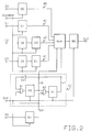
- the processing, serializing and synchronizing device of Fig. 1 has 3 input terminals IN, R2 and CLK at which a digital input signal IN synchronous with a 160 MHz clock signal, a reset signal R2 for instance generated under control of an operator, and a clock signal CLK with a frequency of 160 MHz are applied respectively, and an output terminal OUT where a like named digital output signal synchronous with CLK is provided.
- the device includes a processing circuit P wherein the signal IN is demultiplexed into 4 digital signals which are processed in parallel at a speed of 40 MHz.
- P is reset by a reset signal R1 and controlled by a clock signal CLK4BUF having a frequency of 40 MHz. It generates 4 output signals I0 to I3 which are the processed digital signals and which are applied to respective like named inputs of a serializing and synchronizing device S controlled by the clock signal CLK4BUF, by a reset signal R3 and by the clock signal CLK.
- S generates the output signal OUT.
- the device additionally includes a control circuit C to respective inputs of which the signals R2 and CLK are applied and which generates the reset signals R1 and R3 and the clock signal CLK4BUF.
- the serializing and synchronizing circuit S is shown in more detail in Fig. 2. It includes 4 D-flipflops D0 to D3 having the respective inputs I0 to I3 to which the signals I0 to I3 of P are applied. The outputs of D2 and D3 are connected to an input of D flipflops E0 and E1 respectively. D0, D1, E0 and E1 generate signals d0, d1, e0 and e1 respectively which are applied to distinct inputs of a multiplexer MUX an output of which is connected with an input of a D flipflop B0 which generates the output signal OUT.
- S additionally includes a counter circuit C1 of the well known Johnson type and comprising two D flipflops X0 and X1, 2 AND gates A1 and A2, each with one inverting input, and an invertor IV1.
- An output of XO is via a non-inverting input of A2 coupled to an input of X1 an output of which is via IV1 and a non-inverting input of A1 in series, coupled back to an input of X0.
- the outputs of X0 and X1 are connected to respective control inputs of MUX where respective signals x0 and x1 are applied.
- a reset signal R3' generated by a D flipflop B1 is applied to the inverting input of both A1 and A2, whilst the reset signal R3 from the control circuit C is applied to an input of B1.
- the flipflops D0 to D3, E0 and E1 are controlled by the clock signal CLK4BUF, whilst the other flipflops of S are controlled by CLK.
- C includes a cascade connection of 11 D flipflops AF0, AF1 and B2 to B10.
- the reset signal R2 is applied to an input of AF0 and the reset signal R3 is generated by B10.
- the output of the 9th flipflop B8 is not only connected to B9, but also to an input of a D flipflop B11 which is controlled by CLK4BUF and generates the reset signal R1.
- the 3th and the 4th flipflops B2 and B3 generate signals b2 and b3 respectively which are applied to respective inputs of an XOR gate XOR providing a signal xor.
- B2, B3 and XOR form a detection circuit DT, whilst B4 to B10, and B4 to B8 and B11 constitute 2 delay circuits D1 and D2 respectively.
- C additionally includes a counter circuit DI which is a well known Johnson counter comprising 2 D flipflops C0 and C1, 2 AND gates A3 and A4, each with an inverting input and an invertor IV2.
- DI which is a well known Johnson counter comprising 2 D flipflops C0 and C1, 2 AND gates A3 and A4, each with an inverting input and an invertor IV2.
- An output of C0, where a signal c0 is generated, is coupled to an input of C1 via A4, whilst an output of C1 is coupled back to an input of C0 via IV2 and A3 in series.
- a signal c0 and the clock signal CLK4 are generated respectively.
- the signal xor is applied to the inverting inputs of both A3 and A4 and CLK4 is applied to an input of a buffer circuit B which generates CLK4BUF.
- DT, DI and B form a generator circuit which generates the clock signal CLK4BUF from the clock signal CLK.
- D flipflops of the processing, serializing and synchronizing device are positive edge triggered ones, except E0 and E1.
- the signal R2 which is an asynchronous reset is first synchronized with CLK by the flipflops AF0 and AF1.
- the thus obtained synchronous reset is delayed in B2 and B3, the output signals b2 and b3 of which are compared by means of the XOR gate XOR.
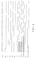
- b2 and b3 are different, i.e. when a signal transition of R2 is detected, xor becomes active as shown in Fig. 4 and resets DI. DI divides the clock signal CLK in 4 thereby generating the clock signal CLK4, which is buffered and thus delayed in B to obtain the clock signal CLK4BUF.
- the signal b3 is by means of B4 to B10, and of B4 to B8, which generates a signal b8, and B11 delayed over 7 clock periods of CLK and over 5 clock periods of CLK plus maximum 1 clock period of CLK4BUF to obtain the reset signals R3 and R1 respectively.
- the latter reset signals are thus delayed over a predetermined time interval with respect to R2 which is such that they do not become active before the clock signal CLK4BUF is stable, whilst the delay of R3 with respect to R1 is such that, after the reset of the processing means P, stable and defined data is present at the input of the multiplexer MUX at the moment the counter circuit C1 is reset by R3.
- flipflop B1 is implemented in the serializing and synchronizing circuit S instead of in C as part of D1, in order to keep the delay of R'3 between the output of B1 and A2 as small as possible.
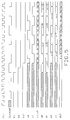
- Figs. 5 and 6 show how the signals I0 to I3 are sampled by MUX and B0 after having been delayed over 1 clock period of CLK4BUF, for I0 and I1, and 1 1/2 clock periods of CLK4BUF for I2 and I3, by D0, D1 and D2,E0; D3, E1 respectively and this again when CLK4BUF equals CLK (Fig. 5) and when CLK4BUF is delayed over 2 1/2 clock period of CLK (Fig. 6).
- meaningful data is not necessarily input data of P, since IN can be delayed by P.
- meaningful data is meant data which is not undefined.
- the meaningful sequenced data bits are indicated on Fig. 5 by n, n+1, n+2, etc. where n is part of d0, n+1 is part of d1, n+2 is part of d3, etc. in a cyclic way.
- phase relations between R1, R3, CLK4 and CLK4BUF realized by C are such that when the relative delay of CLK4BUF with respect to CLK4 remains larger than 0 but smaller than 3 clock periods of CLK, d0, d1, e0 and e1 are stable when being sampled by MUX and B0 and that they are then sampled at a constant absolute instant in time and in the correct sequence, independently of the value of that delay.
- This independency is realized by using R2 to control the generation of CLK4, and CLK4 and CLK4BUF to control the generation of R1.
- phase interval is a theoretical one. Indeed in the above description and in the time diagrams of Figs. 4 to 7 implementation specific time delays such as setup delays, hold delays, etc... have not been taken into account. As a result of these delays, the mentioned interval can in practice be subject to small variations which can be determined experimentally.
Landscapes
- Engineering & Computer Science (AREA)
- Microelectronics & Electronic Packaging (AREA)
- Computer Networks & Wireless Communication (AREA)
- Signal Processing (AREA)
- Synchronisation In Digital Transmission Systems (AREA)
Priority Applications (2)
| Application Number | Priority Date | Filing Date | Title |
|---|---|---|---|
| EP93200442A EP0620662A1 (fr) | 1993-02-16 | 1993-02-16 | Dispositif de traitement, de sérialisation et de synchronisation |
| AU54894/94A AU670345B2 (en) | 1993-02-16 | 1994-02-04 | Reset and synchronizing device |
Applications Claiming Priority (1)
| Application Number | Priority Date | Filing Date | Title |
|---|---|---|---|
| EP93200442A EP0620662A1 (fr) | 1993-02-16 | 1993-02-16 | Dispositif de traitement, de sérialisation et de synchronisation |
Publications (1)
| Publication Number | Publication Date |
|---|---|
| EP0620662A1 true EP0620662A1 (fr) | 1994-10-19 |
Family
ID=8213649
Family Applications (1)
| Application Number | Title | Priority Date | Filing Date |
|---|---|---|---|
| EP93200442A Ceased EP0620662A1 (fr) | 1993-02-16 | 1993-02-16 | Dispositif de traitement, de sérialisation et de synchronisation |
Country Status (2)
| Country | Link |
|---|---|
| EP (1) | EP0620662A1 (fr) |
| AU (1) | AU670345B2 (fr) |
Cited By (2)
| Publication number | Priority date | Publication date | Assignee | Title |
|---|---|---|---|---|
| WO1995010904A1 (fr) * | 1993-10-12 | 1995-04-20 | Telefonaktiebolaget Lm Ericsson | Unite de traitement de signaux |
| WO2001093491A3 (fr) * | 2000-06-02 | 2003-09-04 | Connectcom Microsystems Inc | Emetteur reseau haute frequence |
Citations (1)
| Publication number | Priority date | Publication date | Assignee | Title |
|---|---|---|---|---|
| US3985963A (en) * | 1973-10-03 | 1976-10-12 | Societe Anonyme De Telecommunications | Device for ensuring in an intermediate station the transfer and the branch connection of at least one multiplexed numerical data channel |
-
1993
- 1993-02-16 EP EP93200442A patent/EP0620662A1/fr not_active Ceased
-
1994
- 1994-02-04 AU AU54894/94A patent/AU670345B2/en not_active Ceased
Patent Citations (1)
| Publication number | Priority date | Publication date | Assignee | Title |
|---|---|---|---|---|
| US3985963A (en) * | 1973-10-03 | 1976-10-12 | Societe Anonyme De Telecommunications | Device for ensuring in an intermediate station the transfer and the branch connection of at least one multiplexed numerical data channel |
Non-Patent Citations (3)
| Title |
|---|
| IEEE JOURNAL OF SOLID-STATE CIRCUITS. vol. 23, no. 1, 1 February 1988, NEW YORK US pages 133 - 141 H. JONATHAN CHAO ET AL. 'A 140 Mbit/s CMOS LSI framer chip for a broad-band ISDN local acces system.' * |
| IRE WESCON CONVENTION RECORD vol. 31, 1987, NORTH HOLLYWOOD US pages 300 - 304 RAMESH BHIMARAO 'A GaAs structured cell array for 1.5Gb/s fiber-optic communication applications' * |
| PATENT ABSTRACTS OF JAPAN vol. 01, no. 3023 (E-705)10 January 1989 & JP-A-63 226 121 ( NEC CORP. ) 20 September 1988 * |
Cited By (3)
| Publication number | Priority date | Publication date | Assignee | Title |
|---|---|---|---|---|
| WO1995010904A1 (fr) * | 1993-10-12 | 1995-04-20 | Telefonaktiebolaget Lm Ericsson | Unite de traitement de signaux |
| AU680560B2 (en) * | 1993-10-12 | 1997-07-31 | Telefonaktiebolaget Lm Ericsson (Publ) | Signal processing unit |
| WO2001093491A3 (fr) * | 2000-06-02 | 2003-09-04 | Connectcom Microsystems Inc | Emetteur reseau haute frequence |
Also Published As
| Publication number | Publication date |
|---|---|
| AU5489494A (en) | 1994-08-18 |
| AU670345B2 (en) | 1996-07-11 |
Similar Documents
| Publication | Publication Date | Title |
|---|---|---|
| US5864250A (en) | Non-servo clock and data recovery circuit and method | |
| EP0877505B1 (fr) | Contrôleur de circuit synchrone pour le contrôle de transmission de données entre circuits asynchrones | |
| US5455840A (en) | Method of compensating a phase of a system clock in an information processing system, apparatus employing the same and system clock generator | |
| US20080192871A1 (en) | Method and system of cycle slip framing in a deserializer | |
| US5550878A (en) | Phase comparator | |
| US4876699A (en) | High speed sampled data digital phase detector apparatus | |
| AU657634B2 (en) | High-speed time-multiplexed data transmission system | |
| US4852124A (en) | Digital phase-locked loop clock extractor for bipolar signals | |
| US7260166B2 (en) | Systems for synchronizing resets in multi-clock frequency applications | |
| US5946327A (en) | Method and apparatus for converting between a multi-bit TDM bus and a single-bit TDM bus using digital logic | |
| US3213375A (en) | Synchronized controlled period pulse generator for producing pulses in place of missing input pulses | |
| AU670345B2 (en) | Reset and synchronizing device | |
| US5436628A (en) | Programmable frequency timing generator with phase adjust | |
| US5825834A (en) | Fast response system implementing a sampling clock for extracting stable clock information from a serial data stream with defined jitter characeristics and method therefor | |
| US4317080A (en) | Signal monitor system | |
| US6928573B2 (en) | Communication clocking conversion techniques | |
| US5268653A (en) | Digital phase-locked loop operating mode control method and device | |
| KR100418017B1 (ko) | 데이터 및 클럭 복원회로 | |
| JPS613545A (ja) | 標本化回路 | |
| US20040004505A1 (en) | Data delay circuit | |
| JPH06244739A (ja) | マルチプレクサ回路 | |
| US4855969A (en) | Dynamic timing reference alignment system | |
| JP2798125B2 (ja) | ディジタル信号同期化回路 | |
| US3820051A (en) | Adaptive threshold circuit employing nand gates interconnecting flip-flop circuit | |
| CA1264830A (fr) | Circuit de restitution de donnees et de generation de signaux d'horloge pour appareil de verification de systeme de transmission de donnees |
Legal Events
| Date | Code | Title | Description |
|---|---|---|---|
| PUAI | Public reference made under article 153(3) epc to a published international application that has entered the european phase |
Free format text: ORIGINAL CODE: 0009012 |
|
| AK | Designated contracting states |
Kind code of ref document: A1 Designated state(s): BE DE ES FR GB IT NL SE |
|
| RBV | Designated contracting states (corrected) |
Designated state(s): BE DE ES FR GB IT NL SE |
|
| 17P | Request for examination filed |
Effective date: 19950419 |
|
| RAP1 | Party data changed (applicant data changed or rights of an application transferred) |
Owner name: ALCATEL BELL NAAMLOZE VENNOOTSCHAP |
|
| GRAG | Despatch of communication of intention to grant |
Free format text: ORIGINAL CODE: EPIDOS AGRA |
|
| 17Q | First examination report despatched |
Effective date: 19980609 |
|
| STAA | Information on the status of an ep patent application or granted ep patent |
Free format text: STATUS: THE APPLICATION HAS BEEN REFUSED |
|
| 18R | Application refused |
Effective date: 19981129 |