EP0621500A1 - Beleuchtete transparente Anzeige mit rückseitigem Mikrotextur-Reflektor - Google Patents
Beleuchtete transparente Anzeige mit rückseitigem Mikrotextur-Reflektor Download PDFInfo
- Publication number
- EP0621500A1 EP0621500A1 EP94302586A EP94302586A EP0621500A1 EP 0621500 A1 EP0621500 A1 EP 0621500A1 EP 94302586 A EP94302586 A EP 94302586A EP 94302586 A EP94302586 A EP 94302586A EP 0621500 A1 EP0621500 A1 EP 0621500A1
- Authority
- EP
- European Patent Office
- Prior art keywords
- substrate
- microtextured
- transparent
- reflector
- light
- Prior art date
- Legal status (The legal status is an assumption and is not a legal conclusion. Google has not performed a legal analysis and makes no representation as to the accuracy of the status listed.)
- Withdrawn
Links
- 239000000758 substrate Substances 0.000 claims abstract description 28
- 239000000463 material Substances 0.000 claims description 7
- 229920003023 plastic Polymers 0.000 description 8
- 230000000007 visual effect Effects 0.000 description 7
- 239000004033 plastic Substances 0.000 description 6
- 238000000034 method Methods 0.000 description 4
- 229920002120 photoresistant polymer Polymers 0.000 description 4
- PXHVJJICTQNCMI-UHFFFAOYSA-N Nickel Chemical compound [Ni] PXHVJJICTQNCMI-UHFFFAOYSA-N 0.000 description 3
- 229910052782 aluminium Inorganic materials 0.000 description 3
- XAGFODPZIPBFFR-UHFFFAOYSA-N aluminium Chemical compound [Al] XAGFODPZIPBFFR-UHFFFAOYSA-N 0.000 description 3
- 238000009713 electroplating Methods 0.000 description 3
- 239000004568 cement Substances 0.000 description 2
- 238000010586 diagram Methods 0.000 description 2
- 238000005286 illumination Methods 0.000 description 2
- 239000004973 liquid crystal related substance Substances 0.000 description 2
- 229910052751 metal Inorganic materials 0.000 description 2
- 239000002184 metal Substances 0.000 description 2
- 229920003229 poly(methyl methacrylate) Polymers 0.000 description 2
- 239000004926 polymethyl methacrylate Substances 0.000 description 2
- RYGMFSIKBFXOCR-UHFFFAOYSA-N Copper Chemical compound [Cu] RYGMFSIKBFXOCR-UHFFFAOYSA-N 0.000 description 1
- XUIMIQQOPSSXEZ-UHFFFAOYSA-N Silicon Chemical compound [Si] XUIMIQQOPSSXEZ-UHFFFAOYSA-N 0.000 description 1
- 230000004913 activation Effects 0.000 description 1
- 230000001464 adherent effect Effects 0.000 description 1
- 239000011248 coating agent Substances 0.000 description 1
- 238000000576 coating method Methods 0.000 description 1
- 229910052802 copper Inorganic materials 0.000 description 1
- 239000010949 copper Substances 0.000 description 1
- 239000006185 dispersion Substances 0.000 description 1
- 230000000694 effects Effects 0.000 description 1
- 238000004049 embossing Methods 0.000 description 1
- 239000011888 foil Substances 0.000 description 1
- 230000004313 glare Effects 0.000 description 1
- 238000010438 heat treatment Methods 0.000 description 1
- 230000001788 irregular Effects 0.000 description 1
- 238000004377 microelectronic Methods 0.000 description 1
- 239000000203 mixture Substances 0.000 description 1
- 229910052759 nickel Inorganic materials 0.000 description 1
- 229910052710 silicon Inorganic materials 0.000 description 1
- 239000010703 silicon Substances 0.000 description 1
- 229920002379 silicone rubber Polymers 0.000 description 1
- 239000004945 silicone rubber Substances 0.000 description 1
- 230000000153 supplemental effect Effects 0.000 description 1
- 238000007738 vacuum evaporation Methods 0.000 description 1
Images


Classifications
-
- G—PHYSICS
- G02—OPTICS
- G02B—OPTICAL ELEMENTS, SYSTEMS OR APPARATUS
- G02B6/00—Light guides; Structural details of arrangements comprising light guides and other optical elements, e.g. couplings
- G02B6/0001—Light guides; Structural details of arrangements comprising light guides and other optical elements, e.g. couplings specially adapted for lighting devices or systems
- G02B6/0011—Light guides; Structural details of arrangements comprising light guides and other optical elements, e.g. couplings specially adapted for lighting devices or systems the light guides being planar or of plate-like form
- G02B6/0033—Means for improving the coupling-out of light from the light guide
- G02B6/0035—Means for improving the coupling-out of light from the light guide provided on the surface of the light guide or in the bulk of it
- G02B6/0036—2-D arrangement of prisms, protrusions, indentations or roughened surfaces
-
- G—PHYSICS
- G02—OPTICS
- G02B—OPTICAL ELEMENTS, SYSTEMS OR APPARATUS
- G02B6/00—Light guides; Structural details of arrangements comprising light guides and other optical elements, e.g. couplings
- G02B6/0001—Light guides; Structural details of arrangements comprising light guides and other optical elements, e.g. couplings specially adapted for lighting devices or systems
- G02B6/0011—Light guides; Structural details of arrangements comprising light guides and other optical elements, e.g. couplings specially adapted for lighting devices or systems the light guides being planar or of plate-like form
- G02B6/0033—Means for improving the coupling-out of light from the light guide
- G02B6/0058—Means for improving the coupling-out of light from the light guide varying in density, size, shape or depth along the light guide
- G02B6/0061—Means for improving the coupling-out of light from the light guide varying in density, size, shape or depth along the light guide to provide homogeneous light output intensity
-
- G—PHYSICS
- G02—OPTICS
- G02B—OPTICAL ELEMENTS, SYSTEMS OR APPARATUS
- G02B6/00—Light guides; Structural details of arrangements comprising light guides and other optical elements, e.g. couplings
- G02B6/0001—Light guides; Structural details of arrangements comprising light guides and other optical elements, e.g. couplings specially adapted for lighting devices or systems
- G02B6/0011—Light guides; Structural details of arrangements comprising light guides and other optical elements, e.g. couplings specially adapted for lighting devices or systems the light guides being planar or of plate-like form
- G02B6/0065—Manufacturing aspects; Material aspects
-
- G—PHYSICS
- G02—OPTICS
- G02F—OPTICAL DEVICES OR ARRANGEMENTS FOR THE CONTROL OF LIGHT BY MODIFICATION OF THE OPTICAL PROPERTIES OF THE MEDIA OF THE ELEMENTS INVOLVED THEREIN; NON-LINEAR OPTICS; FREQUENCY-CHANGING OF LIGHT; OPTICAL LOGIC ELEMENTS; OPTICAL ANALOGUE/DIGITAL CONVERTERS
- G02F1/00—Devices or arrangements for the control of the intensity, colour, phase, polarisation or direction of light arriving from an independent light source, e.g. switching, gating or modulating; Non-linear optics
- G02F1/01—Devices or arrangements for the control of the intensity, colour, phase, polarisation or direction of light arriving from an independent light source, e.g. switching, gating or modulating; Non-linear optics for the control of the intensity, phase, polarisation or colour
- G02F1/13—Devices or arrangements for the control of the intensity, colour, phase, polarisation or direction of light arriving from an independent light source, e.g. switching, gating or modulating; Non-linear optics for the control of the intensity, phase, polarisation or colour based on liquid crystals, e.g. single liquid crystal display cells
- G02F1/133—Constructional arrangements; Operation of liquid crystal cells; Circuit arrangements
- G02F1/1333—Constructional arrangements; Manufacturing methods
- G02F1/1335—Structural association of cells with optical devices, e.g. polarisers or reflectors
- G02F1/133553—Reflecting elements
-
- G—PHYSICS
- G02—OPTICS
- G02B—OPTICAL ELEMENTS, SYSTEMS OR APPARATUS
- G02B6/00—Light guides; Structural details of arrangements comprising light guides and other optical elements, e.g. couplings
- G02B6/0001—Light guides; Structural details of arrangements comprising light guides and other optical elements, e.g. couplings specially adapted for lighting devices or systems
- G02B6/0011—Light guides; Structural details of arrangements comprising light guides and other optical elements, e.g. couplings specially adapted for lighting devices or systems the light guides being planar or of plate-like form
- G02B6/0033—Means for improving the coupling-out of light from the light guide
- G02B6/005—Means for improving the coupling-out of light from the light guide provided by one optical element, or plurality thereof, placed on the light output side of the light guide
- G02B6/0051—Diffusing sheet or layer
-
- G—PHYSICS
- G02—OPTICS
- G02B—OPTICAL ELEMENTS, SYSTEMS OR APPARATUS
- G02B6/00—Light guides; Structural details of arrangements comprising light guides and other optical elements, e.g. couplings
- G02B6/0001—Light guides; Structural details of arrangements comprising light guides and other optical elements, e.g. couplings specially adapted for lighting devices or systems
- G02B6/0011—Light guides; Structural details of arrangements comprising light guides and other optical elements, e.g. couplings specially adapted for lighting devices or systems the light guides being planar or of plate-like form
- G02B6/0033—Means for improving the coupling-out of light from the light guide
- G02B6/005—Means for improving the coupling-out of light from the light guide provided by one optical element, or plurality thereof, placed on the light output side of the light guide
- G02B6/0055—Reflecting element, sheet or layer
Definitions
- This invention relates to illuminating devices, and, more particularly, to an illuminating device particularly useful for illuminating transparent displays such as liquid crystal displays (LCD).
- transparent display applicants refer to visual display devices wherein either the visual message portion of the display or the background portion is transparent or translucent.
- LCD displays low power liquid crystal displays
- LCD displays have a number of shortcomings.
- the activated portion is darkened, representing a visual message
- the unactivated portion is transparent, constituting visual background.
- One shortcoming of LCD displays is the relatively low contrast between the activated portion and the unactivated portion. The contrast can be increased by backlighting the cell, thereby producing a sharp visual contrast between the portions of the cell darkened by activation and the light shining through the transparent regions.
- conventional backlighting arrangements are inefficient. Even in so complex an electronic structure as a portable computer, the power used in display backlighting is the major drain on the system batteries.
- a reflector having dispersion characteristics of enhanced uniformity and a display device which can be read over an enhanced range of viewing angles.
- a reflector comprises a base plane having a microtextured surface comprising a pattern of microelements having maximum lateral dimensions less than 125 micrometers and smooth continuous mold-formed surfaces arising from the base plane.
- a preferred reflecting surface is composed of closely packed, smooth- surfaced spherical segments having diameters of twenty-five microns and attitudes of four microns.
- a particularly efficient illuminating device for a transparent display comprises a microtextured reflecting surface formed on a major surface of a transparent substrate and a light source fordirecting light into the transparentsub- strate approximately parallel to the major surface.
- the substrate has two major surfaces separated by a thickness in the range 0.5 to 1.0 mm so that the substrate behaves as a light guide. A substantial portion of the light passing into the substrate undergoes total internal reflection until it hits a microelement and is reflected out of the substrate. The result is an efficient illuminating device particularly useful for lighting transparent displays.
- FIGS. 1 and 2 are schematic enlarged top and cross sectional views respectively of a preferred reflecting surface.
- FIG. 1 shows a greatly enlarged top view of a microtextured reflector 10 comprising a pattern of microelements, each having smooth, continuous, mold-formed surfaces and maximum lateral dimensions along the plane of the surface of less than about 125 micrometers.
- the preferred pattern comprises a mixture of two microelements: spherical segments 11 and random segments 12.
- the bases of the spherical segments, as seen from a top view occupy 50 to 90% of the reflector surface and preferably 50 to 80%.
- the spherical segments occupy on the reflector plane, base circles of diameter in the range 10-125 microns, and preferably they all occupy bases of diameter 25 ⁇ 10 micrometers.
- the altitudes of the spherical segments are within the range 10-20% of the diameters.
- the spherical segments can be randomly distributed but are preferably distributed in approximately an open hexagonal array.
- the random segments 12 are microelements having irregularly shaped bases disposed between successive spherical microelements.
- the random segments preferably have no dimension exceeding 125 micrometers and lateral base dimensions comparable to the base diameters of the spherical segments.
- the rationale for the preferred surface is as follows. If the surface consisted of a close-packed hexagonal array of spherical segments, then ⁇ /2 ⁇ 13 ⁇ 90% of the base plane would be covered by the bases of the spherical segments. However the uniformity of the array could, under some lighting conditions, produce undesirable reflected "rainbow" effects due to diffraction. Moreover if the periodicity of the array were to match the periodicity of the pixels in an overlying LCD display, undesirable moire patterns could occur. However both of these problems can be avoided by randomizing the position of the reflecting segments.
- Preferred, however, is to space the spherical segments apart by about their base diameters and to fill the interstices between them with elements of randomly shaped bases having lateral dimensions comparable to the base diameters of the spherical segments. Since the radii of curvature of these random elements are approximately the same as those of the spherical elements, their reflectance as a function of angle will be nearly the same.
- the spherical segments 11 and random segments 12 are advantageously molded or embossed into a plastic substrate 8, such as polymethyl methacrylate (PMM) coated with a reflecting material 9 such as aluminum.
- PMM polymethyl methacrylate
- a reflecting material 9 such as aluminum.
- the bases of the random segments are irregular, the surfaces 12 extending up from the bases are preferably smooth and continuous.
- FIG. 3 is a schematic cross section of a transparent display using a microtextured back reflector of the type shown in FIGS. 1 and 2.
- the display comprises a transparent dispay cell 30, such as an LCD cell, having a microtextured back reflector 10.
- Reflector 10 is bonded to cell 30 by transparent cement 31 such as transparent silicone rubber cement 31.
- This display is particularly useful as a display screen for a portable telephone where the angle of view is not fixed.
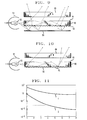
- FIG. 4 is a schematic graphical plot of reflected light intensity of the back reflector 10 versus angle of illumination 0. Viewing at normal incidence is presumed.
- Curve 1 shows the intensity distribution for a conventional isotropic reflector
- Curve 2 shows the intensity distribution for a back reflector of the type shown in FIGS. 1 and 2.
- the back reflector of FIGS. 1 and 2 has a distribution which is relatively flat out to angles of 45° or more, at which angle intensity falls off very rapidly.
- the reflector of FIGS. 1 and 2 when used in the display of FIG. 3 provides greater uniformity over a wider range of viewing angles.
- the range of efficient reflection for the reflector of FIGS. 1 and 2 can be controlled by controlling the ratio of the altitude h of the spherical segments to their base plane diameter d.
- the greater h/d the greater the radius of curvature and the larger the maximum reflected angle 0.
- h/d 1/2 tan 0/4.
- FIG. 5 is a block diagram showing the steps used in making a microtextured reflecting element of the type shown in FIGS. 1 and 2.
- FIG. 6 shows the structures produced at various stages of the FIG. 5 process.
- the first step shown in FIG. 5A is to provide a substrate such as a silicon wafer (60 of FIG. 6).
- the next step is to form on the substrate a planar pattern of photoresist corresponding to the bases of the spherical and random segments to be formed.
- This can be accomplished using conventional photolithographic processing.
- FIG. 6 shows the substrate 60 supporting adherent planar regions of photoresist 61 and 62 corresponding to the bases of spherical and random segments. Preferably the segments have a maximum lateral dimension of less than 125 micrometers.
- the photoresist can be AZ 1300 or AZ 1400 commercially marketed by Shipley Photoresist Co.
- the third step shown in FIG. 5C is to heat the resist to form smooth continuous segments.
- heating developed AZ 1300 spots to 110°C for a period of about 4 minutes produces smooth continuous profiles as shown in FIG. 7.
- the radius of curvature of the spherical segments formed by this process is uniquely determined by the thickness of the resist and the diameter of the base.
- the fourth step is to form an embossing surface or mold conforming to the thus- formed surface. This can be accomplished, for example, by electroplating a few mils of nickel onto the surface of FIG. 7.
- the resulting textured nickel foil can, in turn, be laminated to a copper plate or roll.
- the final step shown in FIG. 5E is to use the textured surface to texture plastic material or metal foil. Plastic, in turn, can be provided with a reflecting surface of aluminum by vacuum evaporation, and the back reflector is complete.
- FIG. 8 illustrates that microtextured reflective elements can be recessed into the body of the reflecting layer rather than projecting out from the body.
- FIG. 8 is a cross section of a reflector wherein the reflective elements are inverted as compared with FIG. 2.
- Inverted spherical segments 71 and random segments 72 arrayed and dimensioned as described in connection with FIGs. 1 and 2 are molded or embossed into plastic substrate 8.
- the plastic is a transparent plastic and reflecting material 79 is selectively applied to the inverted reflective elements to form a transflective device capable of transmitting backlighting in light poor environments and reflecting light in light rich environments.
- the uncoated transparent plastic regions transmit backlighting (not shown) and the reflecting elements 71 and 72 reflect ambient light.
- Such a transflective device is useful as a back reflector in the display of FIG. 3.
- the reflecting material 79 can be selectively applied to the inverted elements by an electroplating process using a sensitizer. After the surface is formed on the plastic, the sensitizer is applied and the surface is subjected to buffing to selectively remove the sensitizer from the non-recessed regions. Electroplating will then selectively deposit reflecting material in the recessed regions where the sensitizer remains.
- FIG. 9 illustrates an illuminating device for providing lighting to a display 89.
- the device comprises a transparent substrate 90 having a pair of major surfaces 91 and 92.
- a microtextured surface is formed on at least one of the major surfaces--preferably the major surface 92 away from display 89.
- a light source comprising a lamp 93 and reflector 94 (preferably paraboloidal in cross section) is provided for directing light into the substrate 90 generally parallel to the microtextured surface 92.
- the substrate 90 preferably has a thickness between the major surfaces of about 0.5 to 1.0 mm so that the substrate acts as a light guide.
- a diffusing surface 95 such as a white sheet is placed near the substrate on the side opposite display 89.
- a diffusing surface 95 such as a white sheet is placed near the substrate on the side opposite display 89.
- FIG. 10 is an alternative embodiment of a low light arrangement similar to that of FIG. 9 except the diffusing surface is omitted and the microtextured surface 92 is provided with a coating 100 of reflecting metal such as aluminum.
- FIG. 11 is a graphical illustration comparing the luminance of the FIG. 10 arrangement (curve 1) with that of a back-lit watch purchased commercially (curve 2).
- the microtextured surface of the FIG. 10 arrangement used spherical segments with 30 micrometer diameter (on the substrate plane) with 35 micrometer center-to-center spacing. The segments extended to a height of about 5 micrometers above the substrate surface.
- the two arrangements employed the same light source.
- FIG. 11 shows that the FIG. 10 arrangement always exceeds the luminance required for reading (the dashed line) and shows a surprisingly enhanced luminance characteristic as compared with the commercial watch.
Landscapes
- Physics & Mathematics (AREA)
- Optics & Photonics (AREA)
- General Physics & Mathematics (AREA)
- Nonlinear Science (AREA)
- Chemical & Material Sciences (AREA)
- Mathematical Physics (AREA)
- Engineering & Computer Science (AREA)
- Crystallography & Structural Chemistry (AREA)
- Manufacturing & Machinery (AREA)
- Optical Elements Other Than Lenses (AREA)
- Liquid Crystal (AREA)
- Planar Illumination Modules (AREA)
- Light Guides In General And Applications Therefor (AREA)
- Devices For Indicating Variable Information By Combining Individual Elements (AREA)
Applications Claiming Priority (2)
| Application Number | Priority Date | Filing Date | Title |
|---|---|---|---|
| US52320 | 1993-04-23 | ||
| US08/052,320 US5349503A (en) | 1991-12-31 | 1993-04-23 | Illuminated transparent display with microtextured back reflector |
Publications (1)
| Publication Number | Publication Date |
|---|---|
| EP0621500A1 true EP0621500A1 (de) | 1994-10-26 |
Family
ID=21976835
Family Applications (1)
| Application Number | Title | Priority Date | Filing Date |
|---|---|---|---|
| EP94302586A Withdrawn EP0621500A1 (de) | 1993-04-23 | 1994-04-13 | Beleuchtete transparente Anzeige mit rückseitigem Mikrotextur-Reflektor |
Country Status (3)
| Country | Link |
|---|---|
| US (1) | US5349503A (de) |
| EP (1) | EP0621500A1 (de) |
| JP (1) | JPH075464A (de) |
Cited By (36)
| Publication number | Priority date | Publication date | Assignee | Title |
|---|---|---|---|---|
| EP0781959A1 (de) * | 1995-12-28 | 1997-07-02 | AT&T Corp. | Transparente Anzeige mit einer Beleuchtungsvorrichtung die einen rückseitigen Mikrotextur-Diffusor aufweist, und Herstellungsverfahren derselben |
| EP0985868A1 (de) * | 1998-09-11 | 2000-03-15 | Gerhard Dipl.-Phys. Karl | Leuchtkörper |
| EP1279891A1 (de) * | 2001-07-27 | 2003-01-29 | Alps Electric Co., Ltd. | Oberflächenemittierende Vorrichtung mit hoher Leuchtfähigkeit, welche auf der Vorderseite einer reflektierenden Flüssigkristallanzeigevorrichtung angebracht ist, und Flüssigkristallanzeigevorrichtung |
| EP1336876A1 (de) * | 2002-02-05 | 2003-08-20 | Alps Electric Co., Ltd. | Beleuchtungsvorrichtung mit Einzellichtquelle und Flüssigkristall Anzeigevorrichtung |
| WO2005114762A1 (fr) * | 2004-05-17 | 2005-12-01 | Thomson Licensing | Diode electroluminescente organique (oled) a extraction de lumiere amelioree, afficheur correspondant |
| WO2006073806A1 (en) * | 2004-12-30 | 2006-07-13 | 3M Innovative Properties Company | Optical film having a surface with rounded structures |
| US7220026B2 (en) | 2004-12-30 | 2007-05-22 | 3M Innovative Properties Company | Optical film having a structured surface with offset prismatic structures |
| US7320538B2 (en) | 2004-12-30 | 2008-01-22 | 3M Innovative Properties Company | Optical film having a structured surface with concave pyramid-shaped structures |
| WO2009154957A3 (en) * | 2008-05-28 | 2010-03-18 | Qualcomm Mems Technologies, Inc. | Light guide panal with light turning microstructure, method of fabrication thereof, and display device |
| US7845841B2 (en) | 2006-08-28 | 2010-12-07 | Qualcomm Mems Technologies, Inc. | Angle sweeping holographic illuminator |
| US7855827B2 (en) | 2006-10-06 | 2010-12-21 | Qualcomm Mems Technologies, Inc. | Internal optical isolation structure for integrated front or back lighting |
| US7864395B2 (en) | 2006-10-27 | 2011-01-04 | Qualcomm Mems Technologies, Inc. | Light guide including optical scattering elements and a method of manufacture |
| US7907319B2 (en) | 1995-11-06 | 2011-03-15 | Qualcomm Mems Technologies, Inc. | Method and device for modulating light with optical compensation |
| US8040589B2 (en) | 2008-02-12 | 2011-10-18 | Qualcomm Mems Technologies, Inc. | Devices and methods for enhancing brightness of displays using angle conversion layers |
| US8049951B2 (en) | 2008-04-15 | 2011-11-01 | Qualcomm Mems Technologies, Inc. | Light with bi-directional propagation |
| US8061882B2 (en) | 2006-10-06 | 2011-11-22 | Qualcomm Mems Technologies, Inc. | Illumination device with built-in light coupler |
| US8068710B2 (en) | 2007-12-07 | 2011-11-29 | Qualcomm Mems Technologies, Inc. | Decoupled holographic film and diffuser |
| US8107155B2 (en) | 2006-10-06 | 2012-01-31 | Qualcomm Mems Technologies, Inc. | System and method for reducing visual artifacts in displays |
| US8169688B2 (en) | 2004-09-27 | 2012-05-01 | Qualcomm Mems Technologies, Inc. | System and method of reducing color shift in a display |
| US8231257B2 (en) | 2009-01-13 | 2012-07-31 | Qualcomm Mems Technologies, Inc. | Large area light panel and screen |
| US8358266B2 (en) | 2008-09-02 | 2013-01-22 | Qualcomm Mems Technologies, Inc. | Light turning device with prismatic light turning features |
| US8373821B2 (en) | 2007-04-30 | 2013-02-12 | Qualcomm Mems Technologies, Inc. | Dual film light guide for illuminating displays |
| CN101881879B (zh) * | 2004-09-27 | 2013-03-13 | 高通Mems科技公司 | 照明干涉式调制器显示器的系统和方法 |
| US8402647B2 (en) | 2010-08-25 | 2013-03-26 | Qualcomm Mems Technologies Inc. | Methods of manufacturing illumination systems |
| US8615912B2 (en) | 2007-06-14 | 2013-12-31 | Avery Dennison Corporation | Illuminated graphical and information display |
| CN103680316A (zh) * | 2013-12-17 | 2014-03-26 | 京东方科技集团股份有限公司 | 透明显示面板及其制造方法、显示装置 |
| US8872085B2 (en) | 2006-10-06 | 2014-10-28 | Qualcomm Mems Technologies, Inc. | Display device having front illuminator with turning features |
| US8902484B2 (en) | 2010-12-15 | 2014-12-02 | Qualcomm Mems Technologies, Inc. | Holographic brightness enhancement film |
| US8928967B2 (en) | 1998-04-08 | 2015-01-06 | Qualcomm Mems Technologies, Inc. | Method and device for modulating light |
| US8971675B2 (en) | 2006-01-13 | 2015-03-03 | Qualcomm Mems Technologies, Inc. | Interconnect structure for MEMS device |
| US8979349B2 (en) | 2009-05-29 | 2015-03-17 | Qualcomm Mems Technologies, Inc. | Illumination devices and methods of fabrication thereof |
| US9019590B2 (en) | 2004-02-03 | 2015-04-28 | Qualcomm Mems Technologies, Inc. | Spatial light modulator with integrated optical compensation structure |
| US9019183B2 (en) | 2006-10-06 | 2015-04-28 | Qualcomm Mems Technologies, Inc. | Optical loss structure integrated in an illumination apparatus |
| US9025235B2 (en) | 2002-12-25 | 2015-05-05 | Qualcomm Mems Technologies, Inc. | Optical interference type of color display having optical diffusion layer between substrate and electrode |
| US9110289B2 (en) | 1998-04-08 | 2015-08-18 | Qualcomm Mems Technologies, Inc. | Device for modulating light with multiple electrodes |
| US20170003437A1 (en) * | 2015-03-03 | 2017-01-05 | Boe Technology Group Co., Ltd. | Composite light guide plate and manufacturing method thereof, backlight module, and display device |
Families Citing this family (42)
| Publication number | Priority date | Publication date | Assignee | Title |
|---|---|---|---|---|
| US5988826A (en) * | 1993-03-25 | 1999-11-23 | Enplas Corporation | Surface light source device |
| DE4425246A1 (de) * | 1994-07-16 | 1996-01-18 | Schoeniger Karl Heinz | Beleuchtete Anzeigetafel |
| US5575549A (en) * | 1994-08-12 | 1996-11-19 | Enplas Corporation | Surface light source device |
| US5521796A (en) * | 1994-09-22 | 1996-05-28 | Taiho Industries Co., Ltd. | Light conducting plate for surface light source device and method for the manufacture thereof |
| US6123877A (en) * | 1994-12-28 | 2000-09-26 | Nashua Corporation | Asymmetric light diffusing material |
| US6712481B2 (en) * | 1995-06-27 | 2004-03-30 | Solid State Opto Limited | Light emitting panel assemblies |
| US5613751A (en) | 1995-06-27 | 1997-03-25 | Lumitex, Inc. | Light emitting panel assemblies |
| US7108414B2 (en) | 1995-06-27 | 2006-09-19 | Solid State Opto Limited | Light emitting panel assemblies |
| US5975711A (en) * | 1995-06-27 | 1999-11-02 | Lumitex, Inc. | Integrated display panel assemblies |
| WO1997008582A1 (en) * | 1995-08-23 | 1997-03-06 | Philips Electronics N.V. | Illumination system for a flat-panel picture display device |
| US5895115A (en) * | 1996-01-16 | 1999-04-20 | Lumitex, Inc. | Light emitting panel assemblies for use in automotive applications and the like |
| EP0882930B1 (de) * | 1996-02-01 | 2010-09-29 | Mitsubishi Rayon Co., Ltd. | Oberflächenlichtquelle und flüssigkristallgerät, signalvorrichtung und diese verwendende signalvorrichtung zur verkehrslenkung |
| US5919551A (en) * | 1996-04-12 | 1999-07-06 | 3M Innovative Properties Company | Variable pitch structured optical film |
| JP4174687B2 (ja) * | 1996-09-24 | 2008-11-05 | セイコーエプソン株式会社 | 照明装置及び液晶表示装置 |
| US5932342A (en) * | 1996-11-14 | 1999-08-03 | Nashua Corporation | Optical diffusers obtained by fluid phase mixing of incompatible materials |
| TW496992B (en) * | 1997-07-29 | 2002-08-01 | Alps Electric Co Ltd | Reflector having pits and projections on a surface thereof, manufacturing method for the same, and reflection type liquid crystal display device using the same |
| JP3257457B2 (ja) | 1997-07-31 | 2002-02-18 | 株式会社日立製作所 | 液晶表示装置 |
| US6007211A (en) * | 1997-09-08 | 1999-12-28 | Cheung; James | Molded illuminating device |
| JP4118389B2 (ja) * | 1997-12-29 | 2008-07-16 | 日本ライツ株式会社 | 導光板および平面照明装置 |
| US7364341B2 (en) * | 1999-02-23 | 2008-04-29 | Solid State Opto Limited | Light redirecting films including non-interlockable optical elements |
| US6827456B2 (en) | 1999-02-23 | 2004-12-07 | Solid State Opto Limited | Transreflectors, transreflector systems and displays and methods of making transreflectors |
| US6752505B2 (en) | 1999-02-23 | 2004-06-22 | Solid State Opto Limited | Light redirecting films and film systems |
| KR100333979B1 (ko) * | 1999-04-26 | 2002-04-24 | 윤종용 | 액정 표시 장치용 박막 트랜지스터 기판 및 그의 제조 방법 |
| US6759281B1 (en) * | 1999-04-26 | 2004-07-06 | Samsung Electronics Co., Ltd. | Method of making a display switch having a contact hole through a passivation layer and a color filter |
| DE19931299C2 (de) * | 1999-07-07 | 2001-08-30 | Philips Corp Intellectual Pty | Bildschirm mit Hintergrundbeleuchtung |
| JP4198281B2 (ja) | 1999-09-13 | 2008-12-17 | 日本ライツ株式会社 | 導光板および平面照明装置 |
| US20060078847A1 (en) * | 2000-09-29 | 2006-04-13 | Kwan Norman H | Dental implant system and additional methods of attachment |
| US7400805B2 (en) * | 2003-06-10 | 2008-07-15 | Abu-Ageel Nayef M | Compact light collection system and method |
| US8324640B2 (en) * | 2004-07-02 | 2012-12-04 | GE Lighting Solutions, LLC | LED-based edge lit illumination system |
| KR101133756B1 (ko) * | 2004-08-30 | 2012-04-09 | 삼성전자주식회사 | 도광판과 이를 구비한 백라이트 어셈블리 및 액정표시장치 |
| EP1828854A4 (de) | 2004-11-04 | 2008-07-30 | Solid State Opto Ltd | Lange gekrümmte keile eines optischen films |
| US20080190071A1 (en) * | 2005-03-31 | 2008-08-14 | Koninklijke Philips Electronics, N.V. | Translucent Wall Element and Motor Vehicle Comprising Such an Element |
| TW200710500A (en) * | 2005-09-09 | 2007-03-16 | Innolux Display Corp | Light guide plate and back light module using the same |
| JP5202906B2 (ja) * | 2007-08-27 | 2013-06-05 | 株式会社ジャパンディスプレイイースト | 液晶表示装置 |
| US20090273852A1 (en) * | 2008-05-02 | 2009-11-05 | U-Tech Media Co., Ltd. | Imaging device with micro-scale optical structures |
| US8462292B2 (en) * | 2008-07-31 | 2013-06-11 | Rambus Delaware Llc | Optically transmissive substrates and light emitting assemblies and methods of making same, and methods of displaying images using the optically transmissive substrates and light emitting assemblies |
| US8500348B2 (en) * | 2008-11-24 | 2013-08-06 | Logitech Europe S.A. | Keyboard with ultra-durable keys |
| US8358508B2 (en) * | 2009-03-19 | 2013-01-22 | Panduit Corp. | Active patch panel |
| CN101865424A (zh) * | 2010-05-14 | 2010-10-20 | 苏州向隆塑胶有限公司 | 导光板、前光模块以及反射式显示装置 |
| GB201008599D0 (en) * | 2010-05-24 | 2010-07-07 | Design Led Products Ltd | Light guide device |
| TWI475974B (zh) * | 2012-01-11 | 2015-03-11 | Global Lighting Technology Inc | 物品展示櫃、透明顯示器與導光板 |
| CN111929944A (zh) * | 2020-09-02 | 2020-11-13 | 京东方科技集团股份有限公司 | 一种显示基板及其制备方法、显示面板、显示模组 |
Citations (6)
| Publication number | Priority date | Publication date | Assignee | Title |
|---|---|---|---|---|
| US3994564A (en) * | 1975-03-31 | 1976-11-30 | Hughes Aircraft Company | Light pipe reflector for use in liquid crystal or other display |
| US4373282A (en) * | 1979-12-26 | 1983-02-15 | Hughes Aircraft Company | Thin-panel illuminator for front-lit displays |
| US4714983A (en) * | 1985-06-10 | 1987-12-22 | Motorola, Inc. | Uniform emission backlight |
| EP0317250A2 (de) * | 1987-11-12 | 1989-05-24 | Mitsubishi Rayon Co., Ltd. | Ebene Lichtquelle |
| JPH04329521A (ja) * | 1991-05-01 | 1992-11-18 | Sharp Corp | 液晶用照明装置 |
| EP0544332A1 (de) * | 1991-11-28 | 1993-06-02 | Enplas Corporation | Flächenartige Lichtquelle |
Family Cites Families (13)
| Publication number | Priority date | Publication date | Assignee | Title |
|---|---|---|---|---|
| US2951419A (en) * | 1953-06-11 | 1960-09-06 | Jerome H Lemelson | Reflective display device |
| US3253971A (en) * | 1962-02-23 | 1966-05-31 | Firestone Tire & Rubber Co | Process of producing product with a reflective surface |
| CH589306A5 (de) * | 1975-06-27 | 1977-06-30 | Bbc Brown Boveri & Cie | |
| JPS5462797A (en) * | 1977-10-28 | 1979-05-21 | Citizen Watch Co Ltd | Liquid crystal color display device |
| US4185895A (en) * | 1978-03-31 | 1980-01-29 | Hughes Aircraft Company | Reflective mode, dynamic scattering liquid crystal display system having a Fresnel reflector for lighting |
| US4431272A (en) * | 1980-05-08 | 1984-02-14 | Kabushiki Kaisha Suwa Seikosha | Liquid crystal display device |
| US4712867A (en) * | 1983-03-09 | 1987-12-15 | Santa Barbara Research Center | Retroreflector |
| DE3605000A1 (de) * | 1985-02-22 | 1986-09-04 | Sharp Kk | Beleuchtungsvorrichtung |
| US4991940A (en) * | 1988-01-25 | 1991-02-12 | Taliq Corporation | Gain reflector-liquid crystal display |
| JP2595067B2 (ja) * | 1988-08-18 | 1997-03-26 | 東ソー株式会社 | 液晶パネル用バックライト |
| US5093765A (en) * | 1990-02-16 | 1992-03-03 | Tosoh Corporation | Back lighting device for a panel |
| US5128787A (en) * | 1990-12-07 | 1992-07-07 | At&T Bell Laboratories | Lcd display with multifaceted back reflector |
| JP2640578B2 (ja) * | 1991-02-27 | 1997-08-13 | シャープ株式会社 | 液晶用照明装置 |
-
1993
- 1993-04-23 US US08/052,320 patent/US5349503A/en not_active Expired - Fee Related
-
1994
- 1994-04-06 JP JP6090749A patent/JPH075464A/ja active Pending
- 1994-04-13 EP EP94302586A patent/EP0621500A1/de not_active Withdrawn
Patent Citations (6)
| Publication number | Priority date | Publication date | Assignee | Title |
|---|---|---|---|---|
| US3994564A (en) * | 1975-03-31 | 1976-11-30 | Hughes Aircraft Company | Light pipe reflector for use in liquid crystal or other display |
| US4373282A (en) * | 1979-12-26 | 1983-02-15 | Hughes Aircraft Company | Thin-panel illuminator for front-lit displays |
| US4714983A (en) * | 1985-06-10 | 1987-12-22 | Motorola, Inc. | Uniform emission backlight |
| EP0317250A2 (de) * | 1987-11-12 | 1989-05-24 | Mitsubishi Rayon Co., Ltd. | Ebene Lichtquelle |
| JPH04329521A (ja) * | 1991-05-01 | 1992-11-18 | Sharp Corp | 液晶用照明装置 |
| EP0544332A1 (de) * | 1991-11-28 | 1993-06-02 | Enplas Corporation | Flächenartige Lichtquelle |
Non-Patent Citations (1)
| Title |
|---|
| PATENT ABSTRACTS OF JAPAN vol. 17, no. 170 (P - 1515) 31 March 1993 (1993-03-31) * |
Cited By (47)
| Publication number | Priority date | Publication date | Assignee | Title |
|---|---|---|---|---|
| US7907319B2 (en) | 1995-11-06 | 2011-03-15 | Qualcomm Mems Technologies, Inc. | Method and device for modulating light with optical compensation |
| EP0781959A1 (de) * | 1995-12-28 | 1997-07-02 | AT&T Corp. | Transparente Anzeige mit einer Beleuchtungsvorrichtung die einen rückseitigen Mikrotextur-Diffusor aufweist, und Herstellungsverfahren derselben |
| US9110289B2 (en) | 1998-04-08 | 2015-08-18 | Qualcomm Mems Technologies, Inc. | Device for modulating light with multiple electrodes |
| US8928967B2 (en) | 1998-04-08 | 2015-01-06 | Qualcomm Mems Technologies, Inc. | Method and device for modulating light |
| EP0985868A1 (de) * | 1998-09-11 | 2000-03-15 | Gerhard Dipl.-Phys. Karl | Leuchtkörper |
| EP1279891A1 (de) * | 2001-07-27 | 2003-01-29 | Alps Electric Co., Ltd. | Oberflächenemittierende Vorrichtung mit hoher Leuchtfähigkeit, welche auf der Vorderseite einer reflektierenden Flüssigkristallanzeigevorrichtung angebracht ist, und Flüssigkristallanzeigevorrichtung |
| US6806922B2 (en) * | 2001-07-27 | 2004-10-19 | Alps Electric Co., Ltd. | Surface light-emitting device having light-guide panel wherein light radiated from exit surface is maximized proximate to normal direction of exit surface |
| EP1336876A1 (de) * | 2002-02-05 | 2003-08-20 | Alps Electric Co., Ltd. | Beleuchtungsvorrichtung mit Einzellichtquelle und Flüssigkristall Anzeigevorrichtung |
| US6734929B2 (en) | 2002-02-05 | 2004-05-11 | Alps Electric Co., Ltd. | Illumination device having a single light source and liquid crystal display device |
| US9025235B2 (en) | 2002-12-25 | 2015-05-05 | Qualcomm Mems Technologies, Inc. | Optical interference type of color display having optical diffusion layer between substrate and electrode |
| US9019590B2 (en) | 2004-02-03 | 2015-04-28 | Qualcomm Mems Technologies, Inc. | Spatial light modulator with integrated optical compensation structure |
| CN100555705C (zh) * | 2004-05-17 | 2009-10-28 | 汤姆森特许公司 | 具有提高的光提取效率的有机发光二极管和对应的显示装置 |
| US7733011B2 (en) | 2004-05-17 | 2010-06-08 | Thomson Licensing | Organic light-emitting diode with relief patterns |
| WO2005114762A1 (fr) * | 2004-05-17 | 2005-12-01 | Thomson Licensing | Diode electroluminescente organique (oled) a extraction de lumiere amelioree, afficheur correspondant |
| CN101881879B (zh) * | 2004-09-27 | 2013-03-13 | 高通Mems科技公司 | 照明干涉式调制器显示器的系统和方法 |
| US8169688B2 (en) | 2004-09-27 | 2012-05-01 | Qualcomm Mems Technologies, Inc. | System and method of reducing color shift in a display |
| US7416309B2 (en) | 2004-12-30 | 2008-08-26 | 3M Innovative Properties Company | Optical film having a surface with rounded structures |
| US7320538B2 (en) | 2004-12-30 | 2008-01-22 | 3M Innovative Properties Company | Optical film having a structured surface with concave pyramid-shaped structures |
| US7220026B2 (en) | 2004-12-30 | 2007-05-22 | 3M Innovative Properties Company | Optical film having a structured surface with offset prismatic structures |
| WO2006073806A1 (en) * | 2004-12-30 | 2006-07-13 | 3M Innovative Properties Company | Optical film having a surface with rounded structures |
| US8971675B2 (en) | 2006-01-13 | 2015-03-03 | Qualcomm Mems Technologies, Inc. | Interconnect structure for MEMS device |
| US7845841B2 (en) | 2006-08-28 | 2010-12-07 | Qualcomm Mems Technologies, Inc. | Angle sweeping holographic illuminator |
| US8107155B2 (en) | 2006-10-06 | 2012-01-31 | Qualcomm Mems Technologies, Inc. | System and method for reducing visual artifacts in displays |
| US9019183B2 (en) | 2006-10-06 | 2015-04-28 | Qualcomm Mems Technologies, Inc. | Optical loss structure integrated in an illumination apparatus |
| US7855827B2 (en) | 2006-10-06 | 2010-12-21 | Qualcomm Mems Technologies, Inc. | Internal optical isolation structure for integrated front or back lighting |
| US8872085B2 (en) | 2006-10-06 | 2014-10-28 | Qualcomm Mems Technologies, Inc. | Display device having front illuminator with turning features |
| US8061882B2 (en) | 2006-10-06 | 2011-11-22 | Qualcomm Mems Technologies, Inc. | Illumination device with built-in light coupler |
| US7864395B2 (en) | 2006-10-27 | 2011-01-04 | Qualcomm Mems Technologies, Inc. | Light guide including optical scattering elements and a method of manufacture |
| US8373821B2 (en) | 2007-04-30 | 2013-02-12 | Qualcomm Mems Technologies, Inc. | Dual film light guide for illuminating displays |
| US8615912B2 (en) | 2007-06-14 | 2013-12-31 | Avery Dennison Corporation | Illuminated graphical and information display |
| US8798425B2 (en) | 2007-12-07 | 2014-08-05 | Qualcomm Mems Technologies, Inc. | Decoupled holographic film and diffuser |
| US8068710B2 (en) | 2007-12-07 | 2011-11-29 | Qualcomm Mems Technologies, Inc. | Decoupled holographic film and diffuser |
| US8040589B2 (en) | 2008-02-12 | 2011-10-18 | Qualcomm Mems Technologies, Inc. | Devices and methods for enhancing brightness of displays using angle conversion layers |
| US8049951B2 (en) | 2008-04-15 | 2011-11-01 | Qualcomm Mems Technologies, Inc. | Light with bi-directional propagation |
| WO2009154957A3 (en) * | 2008-05-28 | 2010-03-18 | Qualcomm Mems Technologies, Inc. | Light guide panal with light turning microstructure, method of fabrication thereof, and display device |
| US8346048B2 (en) | 2008-05-28 | 2013-01-01 | Qualcomm Mems Technologies, Inc. | Front light devices and methods of fabrication thereof |
| CN103149623A (zh) * | 2008-05-28 | 2013-06-12 | 高通Mems科技公司 | 具有光转向微结构的光导面板、其制造方法和显示装置 |
| US8358266B2 (en) | 2008-09-02 | 2013-01-22 | Qualcomm Mems Technologies, Inc. | Light turning device with prismatic light turning features |
| US8439546B2 (en) | 2009-01-13 | 2013-05-14 | Qualcomm Mems Technologies, Inc. | Large area light panel and screen |
| US8231257B2 (en) | 2009-01-13 | 2012-07-31 | Qualcomm Mems Technologies, Inc. | Large area light panel and screen |
| US8979349B2 (en) | 2009-05-29 | 2015-03-17 | Qualcomm Mems Technologies, Inc. | Illumination devices and methods of fabrication thereof |
| US9121979B2 (en) | 2009-05-29 | 2015-09-01 | Qualcomm Mems Technologies, Inc. | Illumination devices and methods of fabrication thereof |
| US8402647B2 (en) | 2010-08-25 | 2013-03-26 | Qualcomm Mems Technologies Inc. | Methods of manufacturing illumination systems |
| US8902484B2 (en) | 2010-12-15 | 2014-12-02 | Qualcomm Mems Technologies, Inc. | Holographic brightness enhancement film |
| CN103680316A (zh) * | 2013-12-17 | 2014-03-26 | 京东方科技集团股份有限公司 | 透明显示面板及其制造方法、显示装置 |
| CN103680316B (zh) * | 2013-12-17 | 2015-09-23 | 京东方科技集团股份有限公司 | 透明显示面板及其制造方法、显示装置 |
| US20170003437A1 (en) * | 2015-03-03 | 2017-01-05 | Boe Technology Group Co., Ltd. | Composite light guide plate and manufacturing method thereof, backlight module, and display device |
Also Published As
| Publication number | Publication date |
|---|---|
| US5349503A (en) | 1994-09-20 |
| JPH075464A (ja) | 1995-01-10 |
Similar Documents
| Publication | Publication Date | Title |
|---|---|---|
| US5349503A (en) | Illuminated transparent display with microtextured back reflector | |
| US5245454A (en) | Lcd display with microtextured back reflector and method for making same | |
| KR101298786B1 (ko) | 조명 조립체 및 시스템 | |
| KR100425348B1 (ko) | 반사체 및 반사형 액정표시장치 | |
| TWI243920B (en) | Light redirecting films and film systems | |
| US5128787A (en) | Lcd display with multifaceted back reflector | |
| US5598280A (en) | Film lens and a surface light source using the same | |
| JP2019513300A (ja) | 光拡散の方法と装置 | |
| TW200907420A (en) | Diffuser prism sheet comprising light diffuser in the valley of prism and LCD back light unit thereby | |
| KR20000029356A (ko) | 반사 및 투과 기능을 갖는 광학판 | |
| US6285425B1 (en) | Ridged reflector for an optical display having a curved and a planar facet for each ridge | |
| US7321407B2 (en) | Reflector and liquid crystal display | |
| EP1916551A1 (de) | Prismamatrix mit Zufallsphasenstrukturen | |
| KR20040086525A (ko) | 반투과 반사막 및 액정 표시 장치 | |
| JP2002207214A (ja) | 反射板並びに反射型液晶表示装置及びその製造方法 | |
| JPWO2001035129A1 (ja) | 反射部材及び光反射方法 | |
| EP1183569A1 (de) | Anzeigevorrichtung und lichtdurchslässige platte dazu | |
| US7567318B2 (en) | Reflector and liquid crystal display panel | |
| JPH117014A (ja) | 照明装置および液晶表示装置および電子機器 | |
| US7057685B2 (en) | Reflective plate, liquid crystal display (LCD) using same, and electronic apparatus using this LCD | |
| CN105223729A (zh) | 一种液晶显示装置 | |
| US20080055936A1 (en) | Light redirecting film having varying optical elements | |
| US20090033829A1 (en) | Prism sheet and liquid crystal display device using the same | |
| JP2002109930A (ja) | 面光源装置 | |
| CN218601642U (zh) | 背光模组以及显示装置 |
Legal Events
| Date | Code | Title | Description |
|---|---|---|---|
| PUAI | Public reference made under article 153(3) epc to a published international application that has entered the european phase |
Free format text: ORIGINAL CODE: 0009012 |
|
| AK | Designated contracting states |
Kind code of ref document: A1 Designated state(s): DE |
|
| K1C1 | Correction of patent application (title page) published |
Effective date: 19941026 |
|
| 17P | Request for examination filed |
Effective date: 19950412 |
|
| 17Q | First examination report despatched |
Effective date: 19970120 |
|
| STAA | Information on the status of an ep patent application or granted ep patent |
Free format text: STATUS: THE APPLICATION IS DEEMED TO BE WITHDRAWN |
|
| 18D | Application deemed to be withdrawn |
Effective date: 19970531 |