EP0621991B1 - Hochspannungsgenerator mit ausgangsstromsteuerung - Google Patents
Hochspannungsgenerator mit ausgangsstromsteuerung Download PDFInfo
- Publication number
- EP0621991B1 EP0621991B1 EP93902568A EP93902568A EP0621991B1 EP 0621991 B1 EP0621991 B1 EP 0621991B1 EP 93902568 A EP93902568 A EP 93902568A EP 93902568 A EP93902568 A EP 93902568A EP 0621991 B1 EP0621991 B1 EP 0621991B1
- Authority
- EP
- European Patent Office
- Prior art keywords
- high voltage
- voltage
- controlled
- current
- series
- Prior art date
- Legal status (The legal status is an assumption and is not a legal conclusion. Google has not performed a legal analysis and makes no representation as to the accuracy of the status listed.)
- Expired - Lifetime
Links
- 239000003990 capacitor Substances 0.000 claims abstract description 33
- 230000007423 decrease Effects 0.000 claims description 6
- 238000010586 diagram Methods 0.000 description 6
- 230000000630 rising effect Effects 0.000 description 5
- 238000004088 simulation Methods 0.000 description 2
- 230000003472 neutralizing effect Effects 0.000 description 1
- 238000007493 shaping process Methods 0.000 description 1
Images


Classifications
-
- G—PHYSICS
- G11—INFORMATION STORAGE
- G11C—STATIC STORES
- G11C16/00—Erasable programmable read-only memories
- G11C16/02—Erasable programmable read-only memories electrically programmable
- G11C16/06—Auxiliary circuits, e.g. for writing into memory
- G11C16/30—Power supply circuits
-
- G—PHYSICS
- G11—INFORMATION STORAGE
- G11C—STATIC STORES
- G11C5/00—Details of stores covered by group G11C11/00
- G11C5/14—Power supply arrangements, e.g. power down, chip selection or deselection, layout of wirings or power grids, or multiple supply levels
- G11C5/145—Applications of charge pumps; Boosted voltage circuits; Clamp circuits therefor
-
- H—ELECTRICITY
- H02—GENERATION; CONVERSION OR DISTRIBUTION OF ELECTRIC POWER
- H02M—APPARATUS FOR CONVERSION BETWEEN AC AND AC, BETWEEN AC AND DC, OR BETWEEN DC AND DC, AND FOR USE WITH MAINS OR SIMILAR POWER SUPPLY SYSTEMS; CONVERSION OF DC OR AC INPUT POWER INTO SURGE OUTPUT POWER; CONTROL OR REGULATION THEREOF
- H02M3/00—Conversion of DC power input into DC power output
- H02M3/02—Conversion of DC power input into DC power output without intermediate conversion into AC
- H02M3/04—Conversion of DC power input into DC power output without intermediate conversion into AC by static converters
- H02M3/06—Conversion of DC power input into DC power output without intermediate conversion into AC by static converters using resistors or capacitors, e.g. potential divider
- H02M3/07—Conversion of DC power input into DC power output without intermediate conversion into AC by static converters using resistors or capacitors, e.g. potential divider using capacitors charged and discharged alternately by semiconductor devices with control electrode, e.g. charge pumps
Definitions
- the invention relates to a high voltage generator comprising a first series of voltage multiplying stages, each stage comprising a diode and a capacitor one terminal of which being connected to the cathode of the respective diode, wherein every cathode of a diode is connected to the anode of the diode of the next voltage multiplying stage, a clock generator which is able to generate clock pulses being 180° out of phase with one another and being supplied alternately to the other terminal of the capacitors of successive voltage multiplying stages, the last diode in the series having a high voltage output and said high voltage output being connected to feed-back means, which modifies said two clock pulses in dependence on the voltage on the high voltage output.
- Such a high voltage generator is known from the European patent application 0,350,462. Said known high voltage generator generates a high voltage pulse for instance to program (E)EPROM-memory cells. Therefore, a voltage of about 5 V is converted in a pulse of about 16 V, which value is sufficient to program (E)EPROM-memory cells. Every voltage multiplying stage functions as a charge pump and after each stage a voltage increase at most equal to the step value of the clock pulse less the threshold voltage of the diodes occurs.
- a disadvantage of said known arrangement is that the high voltage output shows spikes whenever one of both clock pulses switches.
- Japanese patent application JP-A-56.094962 discloses a transformerless type DC/DC converter which is controlled by two reverse-phased clock pulses ⁇ 1 and ⁇ 2.
- the output voltage of the output terminal is entirely determined by PWM-control of the two reverse-phased clock pulses.
- US Patent US-A-5,036,229 discloses an arrangement comprising multiple multiplier stages in a charge pump, which multiplier stages are controlled by clock pulses. The application of several charge pumps in parallel are described.
- the object of the invention is to provide an arrangement neutralizing the disadvantage related to the prior art and the output voltage of which does not show any spikes any more.
- the arrangement according to the invention is therefore characterized in that at least the last capacitor of the multiplying stages is connected to a junction in order to be supplied with a control voltage during operation, said junction being connected to an input of a control circuit having two outputs, said junction also being connected to current charging means, which is controlled by one of said two outputs of the control circuit and by the feed-back means, and to current discharge means controlled by the other of said two outputs of the control circuit, in such a way that when, during operation, the control voltage increases to a first predetermined level the control circuit operates to deactivate said current charging means and to activate said current discharge means, and when the control voltage decreases to a second predetermined level the control circuit operates to deactivate said current discharge means and to activate said current charging means.
- the spikes on the high voltage output may be substantially reduced.
- the high voltage generator is characterized in that said feed-back means comprises a high voltage feed-back circuit connected to the high voltage output, in that the output of the high voltage feed-back circuit is connected to the input of an operational amplifier the other input of which is connected to a reference voltage, in that the current charge means comprises a current source controlled by an output of the operational amplifier, and a first switch which is connected in series with said current source and is controlled by said one of said two outputs of the control circuit, in that the current discharge means comprises a second switch being controlled by said other of said two outputs of the control circuit, and in that the control circuit is said clock generator which is able to generate clock pulses being 180° out of phase with one another at its outputs.
- the voltage multiplier only pumps charge to its output when it is needed there.
- said clock pulses switch in such a way that said first switch controlled by clock pulse is opened and said second switch controlled by clock pulse is closed and when the input voltage decreases below the second predetermined level said clock pulses switch again resulting in closing the first switch and opening of said second switch.
- a second identical high voltage generator is provided, the second identical high voltage generator having voltage multiplying stages being alternately supplied with the clock pulses, however, in a reverse order relative to the order of the high voltage generator, the high voltage outputs of both high voltage generators being connected to one another in such a way, that when one of both high voltage generators does not supply any control current but charges its respective last capacitor the other high voltage generator supplies said control current.
- said feed-back means may comprise a high voltage feed-back circuit connected to the high voltage output, in that the output of the high voltage feed-back circuit is connected to the input of an operational amplifier the other input of which is connected to a reference voltage, in that the current charge means comprises a current source controlled by an output of the operational amplifier, and a first switch which is connected in series with said current source and is controlled by said one of said two outputs of the control circuit, in that the current discharge means comprises a second switch being controlled by said other of said two outputs of the control circuit, in that the control circuit is said clock generator which is able to generate clock pulses being 180° out of phase with one another at its outputs, in that a second series of voltage multiplying stages parallel to the first series of multiplying stages is provided, the second series being identical to the first series, in that the last stage of the second series of multiplying stages is connected to a junction of a series connection of two further switches parallel to the first and second switches and to a further input of the clock generator, the further switches being also
- FIG. 1 shows the invention partly in block diagram.
- the figure shows a voltage multiplier known as such comprising several charge pumps connected in series. Every charge pump consists of a diode Di and a capacitor Ci+1 connected to its cathode. At its other terminal each capacitor receives a clock pulse ( ⁇ 1 or ⁇ 2) generated by an oscillator 3.
- the oscillator 3 generates two clock pulses being 180° out of phase with respect to one another, said clock pulses being supplied alternately to the successive capacitors Ci.
- the diodes D0 ... Dn may be MOS-transistors connected as diodes.
- the last capacitor Cn is not controlled by one of both clock pulses ⁇ 1 or ⁇ 2, but by a control current I1. This provides the possibility to reduce spikes on the high voltage output during switching of the clock pulses ⁇ 1 and ⁇ 2.
- the current control of the last capacitor is provided by means of feed-back means comprising a high voltage feed-back circuit 1, a reference source 2, an operational amplifier A, a current source I1 and two switches S1 and S2 controlled by the clock pulses ⁇ 1 and ⁇ 2.
- the output of the high voltage feed-back circuit 1 is connected to the inverting input of the operational amplifier A, the non-inverting input of which receives a reference voltage (or reference current) from a reference voltage or reference current source 2.
- the output of the operational amplifier A controls the output current of the current source 11.
- the output of the current source 11 is connected to ground (VSS) through two switches S1 and S2 being connected in series and being controlled by ⁇ 1 and ⁇ 2, respectively.
- the junction of the switches S1 and S2 provides the voltage Vn to the last capacitor Cn, as well as the input voltage of the oscillator 3.
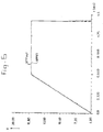
- FIG. 2 shows the voltage Vn to the last capacitor Cn as a function of time. If Vn increases Cn is discharged through Dn and a load connected to the high voltage output HV out . Then, the switch S2 controlled by ⁇ 2 is closed, while the switch S1 controlled by ⁇ 1 is opened. Switch S2 supplies the current I1 to the capacitor Cn, in such a way that the output current I out is also equal to I1. At a certain moment t1 Vn exceeds a predetermined threshold value and the oscillator 3 switches: the outputs ⁇ 1 and ⁇ 2 change sign. The switches S1 and S2 controlled by ⁇ 1 and ⁇ 2, respectively, switch, i.e. S2 opens and S1 closes.
- Vn decreases to ground potential (VSS) the rate of which being determined by the resistance of S1, after which the capacitor Cn is charged through diode Dn-1.
- VSS ground potential
- I1 is a controlled current also the output current I out is a controlled current.
- the voltage Vn has a saw-tooth shape. The slope of the rising edge is determined by I1 being in turn controlled by the high voltage feed-back circuit 1. Since the high voltage feed-back circuit 1 is controlled by the high voltage output HV out the slope of Vn is determined by the load connected to the high voltage output. Furthermore, because Vn also controls the oscillator the frequency of the clock pulses ⁇ 1 and ⁇ 2 is determined by the load. The voltage multiplier, therefore, only pumps charge to the output HV out when it is needed there. So, the voltage multiplier according to the invention does not only have the advantage of having an output being current controlled and having reduced spikes on the output voltage, but also shows frequency control of the oscillator.
- FIG 1 a single multiplying circuit is shown.
- a disadvantage of such a single circuit is that no output current I out can flow during the falling edge of control signal Vn.
- this problem is solved by applying an additional, identical voltage multiplier, in which the voltages ⁇ 1 and ⁇ 2 have inverted values compared to those in the arrangement of figure 1.
- Such a double-phase circuit is shown in figure 1A.
- Figure 3 shows a simulation of a double-phase embodiment of the arrangement according to figure 1.
- Vn1 is equivalent to Vn in figure 1 for one phase and Vn2 for the other phase.
- the frequencies of ⁇ 1 and ⁇ 2 correspond to those of Vn1 and Vn2, respectively.
- VPPID shows the ideal, desired curve of VPP.
- the two other curves show the control signals Vn1 and Vn2. After 60 ⁇ s a heavier load is connected to the output HV out .
- the voltage jump at the beginning of every pulse is caused by the charge pump diode threshold voltage to be exceeded.
- the spikes in the control signals only reach the capacitors being controlled by them, however, they do not reach the output of the charge pump as long as the circuit is properly dimensioned.
- Figures 4, 5 and 6 show resulting programming pulses VPP as a function of time.
- Figure 4 shows VPP in case the last capacitor Cn is not current controlled, but like the other capacitors receives one of both clock pulses ⁇ 1 or ⁇ 2.
- Figure 4 only shows a part of the rising edge of the programming pulse.
- VPP is the output signal of the charge pump, while VPPOUT is the output signal of a (small) low pass filter receiving VPP as input signal.
- Figure 5 shows that in the arrangement according to the invention, applying current control of the last capacitor Cn, spikes caused by the clock pulses are less powerful in the programming pulse VPP.
- FIG. 4 shows an entire programming pulse as may be realized with the arrangement according to the invention. One can clearly see how exactly the real pulse VPPOUT precisely follows the ideal pulse VPPID.
- the invention is not limited to the current control of the last capacitor Cn. Principally, it is possible to control the current of other capacitors. However, generally this results in a lower efficiency of the charge pump. Moreover, then the output current no longer equals 11 and, therefore, this current is defined less well.
Landscapes
- Engineering & Computer Science (AREA)
- Power Engineering (AREA)
- Dc-Dc Converters (AREA)
- Ignition Installations For Internal Combustion Engines (AREA)
- Rectifiers (AREA)
- Details Of Television Scanning (AREA)
- Control Of Eletrric Generators (AREA)
- Direct Current Feeding And Distribution (AREA)
Claims (6)
- Hochspannungsgenerator, der aufweist
eine erste Reihe aus Spannungsvervielfacherstufen, die jeweils eine Diode (D0...Dn) und einen Kondensator (C1...Cn) aufweisen, dessen einer Anschluß mit der Kathode der jeweiligen Diode verbunden ist, wobei jede Kathode einer Diode mit der Anode der Diode der nächsten Spannungsvervielfacherstufe verbunden ist, und
einen Taktgenerator (3), der Taktimpulse (φ1, φ2) erzeugen kann, die gegeneinander um 180° phasenversetzt sind und die abwechselnd dem anderen Anschluß der Kondensatoren der sukzessiven Spannungsvervielfacherstufen eingespeist werden, wobei die letzte Diode in der Reihe einen Hochspannungsausgang hat, welcher mit Rückkoppelgliedern verbunden ist, die die beiden Taktimpulse abhängig von der Spannung (HVout) am Hochspannungsausgang modifizieren, dadurch gekennzeichnet, daß wenigstens der letzte Kondensator (Cn) der Vervielfacherstufen mit einem Verbindungsknoten verbunden ist, um von ihm während des Betriebs mit einer Steuerspannung (Vn) versorgt zu werden, wobei der Verbindungsknoten mit einem Eingang einer Steuerschaltung (3), die zwei Ausgänge hat und auch mit einer von einem der beiden Ausgangssignale der Steuerschaltung (3) und von den Rückkoppelgliedern (1, 2, A) gesteuerten Stromladeeinrichtung (I1, S2) und mit einer Stromentladeeinrichtung (S1) verbunden ist, die von dem anderen der beiden Ausgangssignale der Steuerschaltung (3) derart gesteuert wird, daß, wenn während des Betriebs die Steuerspannung (Vn) auf einen ersten vorgegebenen Pegel wächst, die Steuerschaltung (3) so arbeitet, daß sie die Stromladeeinrichtung (I1, S2) entaktiviert und die Stromentladeeinrichtung (S1) aktiviert, und wenn die Steuerspannung (Vn) auf einen zweiten vorgegebenen Pegel abfällt, die Steuerschaltung (3) so arbeitet, daß sie die Stromentladeeinrichtung (S1) entaktiviert und die Stromladeeinrichtung (I1, S2) aktiviert. - Hochspannungsgenerator nach Anspruch 1, dadurch gekennzeichnet, daß nur der Kondensator (Cn) in der letzten Spannungsvervielfacherstufe mit dem Knoten verbunden ist, und die Steuerspannung (Vn) empfängt.
- Hochspannungsgenerator nach Anspruch 1 oder 2, dadurch gekennzeichnet, daß die Rückkoppelglieder eine mit dem Hochspannungsausgang (HVout) verbundene Hochspannungsrückkoppelschaltung (1) aufweisen,
daß der Ausgang der Hochspannungsrückkoppelschaltung (1) mit dem Eingang eines Operationsverstärkers (A) verbunden ist, dessen anderer Eingang mit einer Referenzspannung verbunden ist,
daß die Stromladeeinrichtung eine von einem Ausgang des Operationsverstärkers (A) gesteuerte Stromquelle (I1) und einen ersten Schalter (S2) aufweist, der in Reihe mit der Stromquelle (I1) verbunden ist und von dem einen der beiden Ausgangssignale der Steuerschaltung (3) gesteuert wird,
daß die Stromentladeeinrichtung einen zweiten Schalter (S1) aufweist, der von dem anderen der beiden Ausgangssignale der Steuerschaltung (3) gesteuert wird, und
daß die Steuerschaltung (3) der Taktgenerator ist, der um 180° gegeneinander phasenversetzte Taktimpulse an seinen Ausgängen erzeugen kann. - Hochspannungsgenerator nach Anspruch 3, dadurch gekennzeichnet, daß, wenn während des Betriebs die Steuerspannung (Vn) den ersten vorgegebenen Pegel überschreitet, die genannten Taktimpulse (φ1, φ2) in der Weise einschalten, daß der vom Taktimpuls (φ2) gesteuerte erste Schalter (S2) geöffnet und der vom Taktimpuls (φ1) gesteuerte zweite Schalter (S1) geschlossen wird, und, wenn die Eingangsspannung unter den zweiten vorgegebenen Pegel abfällt, die Taktimpulse erneut schalten, was im Ergebnis ein Schließen des ersten Schalters (S2) und öffnen des zweiten Schalters (S1) bewirkt.
- Hochspannungsgenerator nach einem der vorangehenden Ansprüche, dadurch gekennzeichnet, daß ein zweiter identischer Hochspannungsgenerator vorgesehen ist, der Hochspannungsvervielfacherstufen hat, die abwechselnd mit den Taktimpulsen (φ1, φ2) gespeist werden, jedoch in umgekehrter Ordnung in Bezug auf die Ordnung des Hochspannungsgenerators, wobei die Hochspannungsausgänge beider Hochspannungsgeneratoren miteinander derart verbunden sind, daß, wenn einer der beiden Hochspannungsgeneratoren überhaupt keinen Strom (I1) liefert, sondern seinen jeweils letzten Kondensator lädt, der andere Hochspannungsgenerator den Steuerstrom (I1) liefert.
- Hochspannungsgenerator nach Anspruch 5, dadurch gekennzeichnet, daß die Rückkoppelglieder eine mit dem Hochspannungsausgang (HVout) verbundene Hochspannungsrückkoppelschaltung (1) aufweisen, daß der Ausgang der Hochspannungsrückkoppelschaltung (1) mit dem Eingang eines Operationsverstärkers (A) verbunden ist, dessen anderer Eingang mit einer Referenzspannung verbunden ist,
daß die Stromladeeinrichtung eine von einem Ausgangssignal des Operationsverstärkers (A) gesteuerte Stromquelle (I1) und einen ersten Schalter (S2) aufweist, der mit der Stromquelle (I1) in Reihe geschaltet ist und von dem einen der beiden Ausgangssignale der Steuerschaltung (3) angesteuert wird,
daß die Stromentladeeinrichtung einen zweiten, von dem anderen der beiden Ausgangssignale der Steuerschaltung (3) angesteuerten Schalter (S1) aufweist,
daß die Steuerschaltung (3) der genannte Taktgenerator ist, der um 180° gegeneinander phasenversetzte Taktimpulse an seinen Ausgängen erzeugen kann,
daß eine zweite Reihe von Spannungsvervielfacherstufen parallel zur ersten Reihe der Spannungsvervielfacherstufen vorgesehen ist, wobei die zweite Reihe mit der ersten Reihe identisch ist, daß die letzte Stufe der zweiten Reihe der Spannungsvervielfacherstufen mit einem Verbindungsknoten einer Reihenschaltung aus zwei weiteren Schaltern parallel zu dem ersten Schalter (S2) und dem zweiten Schalter (S1) und mit einem weiteren Eingang des Taktgenerators (3) verbunden ist, wobei die weiteren Schalter auch von den genannten Taktimpulsen (φ1, φ2) jedoch in umgekehrter Ordnung angesteuert werden.
Applications Claiming Priority (3)
| Application Number | Priority Date | Filing Date | Title |
|---|---|---|---|
| NL9200056 | 1992-01-14 | ||
| NL9200056A NL9200056A (nl) | 1992-01-14 | 1992-01-14 | Hoogspanningsgenerator met uitgangsstroomregeling. |
| PCT/NL1992/000237 WO1993014554A1 (en) | 1992-01-14 | 1992-12-29 | High voltage generator having output current control |
Publications (2)
| Publication Number | Publication Date |
|---|---|
| EP0621991A1 EP0621991A1 (de) | 1994-11-02 |
| EP0621991B1 true EP0621991B1 (de) | 1995-11-08 |
Family
ID=19860290
Family Applications (1)
| Application Number | Title | Priority Date | Filing Date |
|---|---|---|---|
| EP93902568A Expired - Lifetime EP0621991B1 (de) | 1992-01-14 | 1992-12-29 | Hochspannungsgenerator mit ausgangsstromsteuerung |
Country Status (9)
| Country | Link |
|---|---|
| US (1) | US5483434A (de) |
| EP (1) | EP0621991B1 (de) |
| JP (1) | JPH07502879A (de) |
| KR (1) | KR950700632A (de) |
| AT (1) | ATE130133T1 (de) |
| CA (1) | CA2127995A1 (de) |
| DE (1) | DE69205997T2 (de) |
| NL (1) | NL9200056A (de) |
| WO (1) | WO1993014554A1 (de) |
Families Citing this family (61)
| Publication number | Priority date | Publication date | Assignee | Title |
|---|---|---|---|---|
| US5365121A (en) | 1993-03-08 | 1994-11-15 | Motorola Inc. | Charge pump with controlled ramp rate |
| EP0691729A3 (de) * | 1994-06-30 | 1996-08-14 | Sgs Thomson Microelectronics | Ladungspumpenschaltung mit Rückkopplungssteuerung |
| DE19612443C2 (de) * | 1996-03-28 | 1998-02-05 | Siemens Ag | Schaltungsanordnung zur Versorgung eines elektronischen Lastkreises |
| US5907484A (en) * | 1996-04-25 | 1999-05-25 | Programmable Microelectronics Corp. | Charge pump |
| US5774348A (en) * | 1996-06-24 | 1998-06-30 | The United States Of America As Represented By The United States Department Of Energy | Light-weight DC to very high voltage DC converter |
| FR2768573B1 (fr) * | 1997-09-12 | 1999-11-26 | Sgs Thomson Microelectronics | Circuit generateur de tension du type pompe de charge, avec circuit de commande auto-oscillant |
| DE19748577C1 (de) * | 1997-11-04 | 1999-01-21 | Bosch Gmbh Robert | Ladungspumpe |
| DE19834428C2 (de) * | 1998-07-30 | 2001-07-12 | Infineon Technologies Ag | Spannungsvervielfacherschaltung |
| FR2782421B1 (fr) * | 1998-08-11 | 2000-09-15 | St Microelectronics Sa | Dispositif de generation d'une haute tension |
| DE10017920A1 (de) * | 2000-04-11 | 2001-10-25 | Infineon Technologies Ag | Ladungspumpenanordnung |
| US6696882B1 (en) * | 2000-06-22 | 2004-02-24 | Artesyn Technologies, Inc. | Transient override circuit for a voltage regulator circuit |
| US6967523B2 (en) * | 2000-11-21 | 2005-11-22 | Mosaid Technologies Incorporated | Cascaded charge pump power supply with different gate oxide thickness transistors |
| US6927441B2 (en) * | 2001-03-20 | 2005-08-09 | Stmicroelectronics S.R.L. | Variable stage charge pump |
| US6750589B2 (en) * | 2002-01-24 | 2004-06-15 | Honeywell International Inc. | Method and circuit for the control of large arrays of electrostatic actuators |
| US7941675B2 (en) * | 2002-12-31 | 2011-05-10 | Burr James B | Adaptive power control |
| US7112978B1 (en) | 2002-04-16 | 2006-09-26 | Transmeta Corporation | Frequency specific closed loop feedback control of integrated circuits |
| US7949864B1 (en) * | 2002-12-31 | 2011-05-24 | Vjekoslav Svilan | Balanced adaptive body bias control |
| US7953990B2 (en) * | 2002-12-31 | 2011-05-31 | Stewart Thomas E | Adaptive power control based on post package characterization of integrated circuits |
| US7228242B2 (en) | 2002-12-31 | 2007-06-05 | Transmeta Corporation | Adaptive power control based on pre package characterization of integrated circuits |
| US7142040B2 (en) * | 2003-03-27 | 2006-11-28 | Device Engineering Co., Ltd. | Stabilized power supply circuit |
| US7719343B2 (en) | 2003-09-08 | 2010-05-18 | Peregrine Semiconductor Corporation | Low noise charge pump method and apparatus |
| US7692477B1 (en) * | 2003-12-23 | 2010-04-06 | Tien-Min Chen | Precise control component for a substrate potential regulation circuit |
| US7129771B1 (en) | 2003-12-23 | 2006-10-31 | Transmeta Corporation | Servo loop for well bias voltage source |
| US7649402B1 (en) * | 2003-12-23 | 2010-01-19 | Tien-Min Chen | Feedback-controlled body-bias voltage source |
| US7012461B1 (en) | 2003-12-23 | 2006-03-14 | Transmeta Corporation | Stabilization component for a substrate potential regulation circuit |
| US7562233B1 (en) | 2004-06-22 | 2009-07-14 | Transmeta Corporation | Adaptive control of operating and body bias voltages |
| US7774625B1 (en) | 2004-06-22 | 2010-08-10 | Eric Chien-Li Sheng | Adaptive voltage control by accessing information stored within and specific to a microprocessor |
| JP4666345B2 (ja) * | 2004-11-05 | 2011-04-06 | ローム株式会社 | チャージポンプ回路 |
| JP4750530B2 (ja) | 2005-10-27 | 2011-08-17 | ルネサスエレクトロニクス株式会社 | 半導体集積回路装置及びそれを用いた非接触電子装置 |
| US8044705B2 (en) * | 2007-08-28 | 2011-10-25 | Sandisk Technologies Inc. | Bottom plate regulation of charge pumps |
| US7969235B2 (en) * | 2008-06-09 | 2011-06-28 | Sandisk Corporation | Self-adaptive multi-stage charge pump |
| US8710907B2 (en) * | 2008-06-24 | 2014-04-29 | Sandisk Technologies Inc. | Clock generator circuit for a charge pump |
| US9660590B2 (en) | 2008-07-18 | 2017-05-23 | Peregrine Semiconductor Corporation | Low-noise high efficiency bias generation circuits and method |
| US8816659B2 (en) | 2010-08-06 | 2014-08-26 | Peregrine Semiconductor Corporation | Low-noise high efficiency bias generation circuits and method |
| US7795952B2 (en) * | 2008-12-17 | 2010-09-14 | Sandisk Corporation | Regulation of recovery rates in charge pumps |
| DE102009010550A1 (de) * | 2009-02-25 | 2010-09-02 | Texas Instruments Deutschland Gmbh | Ladungspumpe mit Selbsttaktung und Verfahren |
| US7973592B2 (en) * | 2009-07-21 | 2011-07-05 | Sandisk Corporation | Charge pump with current based regulation |
| US8339183B2 (en) * | 2009-07-24 | 2012-12-25 | Sandisk Technologies Inc. | Charge pump with reduced energy consumption through charge sharing and clock boosting suitable for high voltage word line in flash memories |
| US20110133820A1 (en) * | 2009-12-09 | 2011-06-09 | Feng Pan | Multi-Stage Charge Pump with Variable Number of Boosting Stages |
| US20110148509A1 (en) * | 2009-12-17 | 2011-06-23 | Feng Pan | Techniques to Reduce Charge Pump Overshoot |
| US8339185B2 (en) | 2010-12-20 | 2012-12-25 | Sandisk 3D Llc | Charge pump system that dynamically selects number of active stages |
| US8294509B2 (en) | 2010-12-20 | 2012-10-23 | Sandisk Technologies Inc. | Charge pump systems with reduction in inefficiencies due to charge sharing between capacitances |
| US8686787B2 (en) | 2011-05-11 | 2014-04-01 | Peregrine Semiconductor Corporation | High voltage ring pump with inverter stages and voltage boosting stages |
| US9768683B2 (en) | 2011-01-18 | 2017-09-19 | Peregrine Semiconductor Corporation | Differential charge pump |
| US9264053B2 (en) * | 2011-01-18 | 2016-02-16 | Peregrine Semiconductor Corporation | Variable frequency charge pump |
| US8699247B2 (en) | 2011-09-09 | 2014-04-15 | Sandisk Technologies Inc. | Charge pump system dynamically reconfigurable for read and program |
| US8400212B1 (en) | 2011-09-22 | 2013-03-19 | Sandisk Technologies Inc. | High voltage charge pump regulation system with fine step adjustment |
| US8514628B2 (en) | 2011-09-22 | 2013-08-20 | Sandisk Technologies Inc. | Dynamic switching approach to reduce area and power consumption of high voltage charge pumps |
| KR101237843B1 (ko) * | 2011-11-11 | 2013-02-27 | 한밭대학교 산학협력단 | 낮은 배터리 전압의 승압을 위한 전기자동차용 DCtoDC컨버터 장치 |
| US8710909B2 (en) | 2012-09-14 | 2014-04-29 | Sandisk Technologies Inc. | Circuits for prevention of reverse leakage in Vth-cancellation charge pumps |
| US8836412B2 (en) | 2013-02-11 | 2014-09-16 | Sandisk 3D Llc | Charge pump with a power-controlled clock buffer to reduce power consumption and output voltage ripple |
| US8981835B2 (en) | 2013-06-18 | 2015-03-17 | Sandisk Technologies Inc. | Efficient voltage doubler |
| US9024680B2 (en) | 2013-06-24 | 2015-05-05 | Sandisk Technologies Inc. | Efficiency for charge pumps with low supply voltages |
| US9077238B2 (en) | 2013-06-25 | 2015-07-07 | SanDisk Technologies, Inc. | Capacitive regulation of charge pumps without refresh operation interruption |
| US9007046B2 (en) | 2013-06-27 | 2015-04-14 | Sandisk Technologies Inc. | Efficient high voltage bias regulation circuit |
| US9083231B2 (en) | 2013-09-30 | 2015-07-14 | Sandisk Technologies Inc. | Amplitude modulation for pass gate to improve charge pump efficiency |
| US9154027B2 (en) | 2013-12-09 | 2015-10-06 | Sandisk Technologies Inc. | Dynamic load matching charge pump for reduced current consumption |
| GB201506579D0 (en) | 2015-04-17 | 2015-06-03 | Dialog Semiconductor Uk Ltd | Charge pump |
| US9917507B2 (en) | 2015-05-28 | 2018-03-13 | Sandisk Technologies Llc | Dynamic clock period modulation scheme for variable charge pump load currents |
| US9647536B2 (en) | 2015-07-28 | 2017-05-09 | Sandisk Technologies Llc | High voltage generation using low voltage devices |
| US9520776B1 (en) | 2015-09-18 | 2016-12-13 | Sandisk Technologies Llc | Selective body bias for charge pump transfer switches |
Family Cites Families (6)
| Publication number | Priority date | Publication date | Assignee | Title |
|---|---|---|---|---|
| JPS5694962A (en) * | 1979-12-28 | 1981-07-31 | Fujitsu Ltd | Transformerless type dc/dc converter |
| US5006974A (en) * | 1987-12-24 | 1991-04-09 | Waferscale Integration Inc. | On-chip high voltage generator and regulator in an integrated circuit |
| US4979088A (en) * | 1988-12-26 | 1990-12-18 | Matsushita Electric Industrial Co., Ltd. | Integrated high voltage generating system |
| US5036229A (en) * | 1989-07-18 | 1991-07-30 | Gazelle Microcircuits, Inc. | Low ripple bias voltage generator |
| US5175706A (en) * | 1989-12-07 | 1992-12-29 | Sgs-Thomson Microelectronics S.A. | Programming voltage generator circuit for programmable memory |
| US5412257A (en) * | 1992-10-20 | 1995-05-02 | United Memories, Inc. | High efficiency N-channel charge pump having a primary pump and a non-cascaded secondary pump |
-
1992
- 1992-01-14 NL NL9200056A patent/NL9200056A/nl not_active Application Discontinuation
- 1992-12-29 DE DE69205997T patent/DE69205997T2/de not_active Expired - Fee Related
- 1992-12-29 WO PCT/NL1992/000237 patent/WO1993014554A1/en not_active Ceased
- 1992-12-29 JP JP5512342A patent/JPH07502879A/ja active Pending
- 1992-12-29 CA CA002127995A patent/CA2127995A1/en not_active Abandoned
- 1992-12-29 AT AT93902568T patent/ATE130133T1/de not_active IP Right Cessation
- 1992-12-29 US US08/256,511 patent/US5483434A/en not_active Expired - Fee Related
- 1992-12-29 EP EP93902568A patent/EP0621991B1/de not_active Expired - Lifetime
-
1994
- 1994-07-12 KR KR1019940702411A patent/KR950700632A/ko not_active Withdrawn
Also Published As
| Publication number | Publication date |
|---|---|
| WO1993014554A1 (en) | 1993-07-22 |
| JPH07502879A (ja) | 1995-03-23 |
| CA2127995A1 (en) | 1993-07-22 |
| EP0621991A1 (de) | 1994-11-02 |
| US5483434A (en) | 1996-01-09 |
| DE69205997D1 (de) | 1995-12-14 |
| DE69205997T2 (de) | 1996-04-04 |
| KR950700632A (ko) | 1995-01-16 |
| NL9200056A (nl) | 1993-08-02 |
| ATE130133T1 (de) | 1995-11-15 |
Similar Documents
| Publication | Publication Date | Title |
|---|---|---|
| US5483434A (en) | High voltage generator having output current control | |
| US5036229A (en) | Low ripple bias voltage generator | |
| US6794927B2 (en) | Modular charge pump architecture | |
| EP0694184B1 (de) | Aufwärtskonverter mit verlustreduziertestromversorgung, steuerschaltung und dasverfahren dafür | |
| EP3202025B1 (de) | Gleichstromaufwärtsregler mit mehreren ausgängen | |
| JP3467679B2 (ja) | Dc/dc変換器 | |
| US4186336A (en) | Limit cycling regulator apparatus for plural parallel power sources | |
| JP2003289666A (ja) | スイッチング電源回路 | |
| US20040150439A1 (en) | Constant deadtime control in a feed forward enabled pulse width modulator controller | |
| EP4178097B1 (de) | Dreistufiger aufwärtswandler und steuerungsverfahren | |
| EP0822478A3 (de) | Spannungswandlerschaltung und mehrphasiger Taktgenerator | |
| KR980004932A (ko) | 독립적인 웰 바이어스 전압을 가진 전압 펌프 회로 | |
| CN102594123A (zh) | 开关电源的控制电路、控制方法及开关电源、电子设备 | |
| US6753623B2 (en) | Switched capacitor array circuits having universal rest state and method | |
| US7492136B2 (en) | Multi-phase converter with improved load step-up transient response | |
| EP1635444B1 (de) | Abschaltvorrichtung für Ladungspumpeschaltung | |
| US5438504A (en) | Voltage multiplier circuits or the like | |
| US20020159282A1 (en) | Electrical power supply converter | |
| US4302804A (en) | DC Voltage multiplier using phase-sequenced CMOS switches | |
| US20040135564A1 (en) | Switching mode voltage regulator and method thereof | |
| US11594959B1 (en) | Switched capacitor circuit with passive charge recycling | |
| US7304529B2 (en) | Method of controlling a charge pump generator and a related charge pump generator | |
| KR101530397B1 (ko) | 커패시터 직렬접속 제어 기반의 미약 전력 재활용 충전장치 | |
| KR20150050540A (ko) | 커패시터 직렬접속 제어 기반의 미약 전력 재활용 충전장치 | |
| US5798914A (en) | Power factor of a rectified power supply |
Legal Events
| Date | Code | Title | Description |
|---|---|---|---|
| PUAI | Public reference made under article 153(3) epc to a published international application that has entered the european phase |
Free format text: ORIGINAL CODE: 0009012 |
|
| 17P | Request for examination filed |
Effective date: 19940713 |
|
| AK | Designated contracting states |
Kind code of ref document: A1 Designated state(s): AT BE CH DE DK ES FR GB GR IE IT LI LU MC NL PT SE |
|
| 17Q | First examination report despatched |
Effective date: 19950202 |
|
| GRAA | (expected) grant |
Free format text: ORIGINAL CODE: 0009210 |
|
| AK | Designated contracting states |
Kind code of ref document: B1 Designated state(s): AT BE CH DE DK ES FR GB GR IE IT LI LU MC NL PT SE |
|
| PG25 | Lapsed in a contracting state [announced via postgrant information from national office to epo] |
Ref country code: MC Free format text: LAPSE BECAUSE OF NON-PAYMENT OF DUE FEES Effective date: 19951108 Ref country code: IT Free format text: LAPSE BECAUSE OF FAILURE TO SUBMIT A TRANSLATION OF THE DESCRIPTION OR TO PAY THE FEE WITHIN THE PRE;WARNING: LAPSES OF ITALIAN PATENTS WITH EFFECTIVE DATE BEFORE 2007 MAY HAVE OCCURRED AT ANY TIME BEFORE 2007. THE CORRECT EFFECTIVE DATE MAY BE DIFFERENT FROM THE ONE RECORDED.SCRIBED TIME-LIMIT Effective date: 19951108 Ref country code: GR Free format text: LAPSE BECAUSE OF FAILURE TO SUBMIT A TRANSLATION OF THE DESCRIPTION OR TO PAY THE FEE WITHIN THE PRESCRIBED TIME-LIMIT Effective date: 19951108 Ref country code: ES Free format text: THE PATENT HAS BEEN ANNULLED BY A DECISION OF A NATIONAL AUTHORITY Effective date: 19951108 Ref country code: DK Effective date: 19951108 |
|
| REF | Corresponds to: |
Ref document number: 130133 Country of ref document: AT Date of ref document: 19951115 Kind code of ref document: T |
|
| REG | Reference to a national code |
Ref country code: IE Ref legal event code: FG4D Free format text: 66079 |
|
| REF | Corresponds to: |
Ref document number: 69205997 Country of ref document: DE Date of ref document: 19951214 |
|
| PG25 | Lapsed in a contracting state [announced via postgrant information from national office to epo] |
Ref country code: LU Free format text: LAPSE BECAUSE OF NON-PAYMENT OF DUE FEES Effective date: 19951231 Ref country code: IE Free format text: LAPSE BECAUSE OF NON-PAYMENT OF DUE FEES Effective date: 19951231 |
|
| PGFP | Annual fee paid to national office [announced via postgrant information from national office to epo] |
Ref country code: CH Payment date: 19951231 Year of fee payment: 4 |
|
| ET | Fr: translation filed | ||
| REG | Reference to a national code |
Ref country code: CH Ref legal event code: PL |
|
| PGFP | Annual fee paid to national office [announced via postgrant information from national office to epo] |
Ref country code: FR Payment date: 19960624 Year of fee payment: 4 |
|
| PGFP | Annual fee paid to national office [announced via postgrant information from national office to epo] |
Ref country code: BE Payment date: 19960625 Year of fee payment: 4 Ref country code: SE Payment date: 19960625 Year of fee payment: 4 |
|
| PGFP | Annual fee paid to national office [announced via postgrant information from national office to epo] |
Ref country code: DE Payment date: 19960626 Year of fee payment: 4 |
|
| PGFP | Annual fee paid to national office [announced via postgrant information from national office to epo] |
Ref country code: AT Payment date: 19960627 Year of fee payment: 4 |
|
| PLBE | No opposition filed within time limit |
Free format text: ORIGINAL CODE: 0009261 |
|
| STAA | Information on the status of an ep patent application or granted ep patent |
Free format text: STATUS: NO OPPOSITION FILED WITHIN TIME LIMIT |
|
| 26N | No opposition filed | ||
| PG25 | Lapsed in a contracting state [announced via postgrant information from national office to epo] |
Ref country code: GB Effective date: 19961229 Ref country code: AT Effective date: 19961229 |
|
| PG25 | Lapsed in a contracting state [announced via postgrant information from national office to epo] |
Ref country code: SE Effective date: 19961230 |
|
| PG25 | Lapsed in a contracting state [announced via postgrant information from national office to epo] |
Ref country code: LI Free format text: LAPSE BECAUSE OF FAILURE TO SUBMIT A TRANSLATION OF THE DESCRIPTION OR TO PAY THE FEE WITHIN THE PRESCRIBED TIME-LIMIT Effective date: 19961231 Ref country code: CH Free format text: LAPSE BECAUSE OF FAILURE TO SUBMIT A TRANSLATION OF THE DESCRIPTION OR TO PAY THE FEE WITHIN THE PRESCRIBED TIME-LIMIT Effective date: 19961231 Ref country code: BE Effective date: 19961231 |
|
| BERE | Be: lapsed |
Owner name: SIERRA SEMICONDUCTOR B.V. Effective date: 19961231 |
|
| PG25 | Lapsed in a contracting state [announced via postgrant information from national office to epo] |
Ref country code: NL Effective date: 19970701 |
|
| GBPC | Gb: european patent ceased through non-payment of renewal fee |
Effective date: 19961229 |
|
| PG25 | Lapsed in a contracting state [announced via postgrant information from national office to epo] |
Ref country code: FR Effective date: 19970829 |
|
| NLV4 | Nl: lapsed or anulled due to non-payment of the annual fee |
Effective date: 19970701 |
|
| PG25 | Lapsed in a contracting state [announced via postgrant information from national office to epo] |
Ref country code: DE Effective date: 19970902 |
|
| EUG | Se: european patent has lapsed |
Ref document number: 93902568.0 |
|
| REG | Reference to a national code |
Ref country code: FR Ref legal event code: ST |
|
| PG25 | Lapsed in a contracting state [announced via postgrant information from national office to epo] |
Ref country code: PT Free format text: LAPSE BECAUSE OF NON-PAYMENT OF DUE FEES Effective date: 19960408 |