EP0622754B1 - Tafel mit integrierter Anzeige mit hoher Koordinatendetektionsgenauigkeit und Verfahren zur ihrer Steuerung - Google Patents
Tafel mit integrierter Anzeige mit hoher Koordinatendetektionsgenauigkeit und Verfahren zur ihrer Steuerung Download PDFInfo
- Publication number
- EP0622754B1 EP0622754B1 EP94303127A EP94303127A EP0622754B1 EP 0622754 B1 EP0622754 B1 EP 0622754B1 EP 94303127 A EP94303127 A EP 94303127A EP 94303127 A EP94303127 A EP 94303127A EP 0622754 B1 EP0622754 B1 EP 0622754B1
- Authority
- EP
- European Patent Office
- Prior art keywords
- electrode
- signal
- electrodes
- display
- row
- Prior art date
- Legal status (The legal status is an assumption and is not a legal conclusion. Google has not performed a legal analysis and makes no representation as to the accuracy of the status listed.)
- Expired - Lifetime
Links
Images


Classifications
-
- G—PHYSICS
- G06—COMPUTING OR CALCULATING; COUNTING
- G06F—ELECTRIC DIGITAL DATA PROCESSING
- G06F3/00—Input arrangements for transferring data to be processed into a form capable of being handled by the computer; Output arrangements for transferring data from processing unit to output unit, e.g. interface arrangements
- G06F3/01—Input arrangements or combined input and output arrangements for interaction between user and computer
- G06F3/03—Arrangements for converting the position or the displacement of a member into a coded form
- G06F3/041—Digitisers, e.g. for touch screens or touch pads, characterised by the transducing means
- G06F3/0412—Digitisers structurally integrated in a display
-
- G—PHYSICS
- G06—COMPUTING OR CALCULATING; COUNTING
- G06F—ELECTRIC DIGITAL DATA PROCESSING
- G06F3/00—Input arrangements for transferring data to be processed into a form capable of being handled by the computer; Output arrangements for transferring data from processing unit to output unit, e.g. interface arrangements
- G06F3/01—Input arrangements or combined input and output arrangements for interaction between user and computer
- G06F3/03—Arrangements for converting the position or the displacement of a member into a coded form
- G06F3/041—Digitisers, e.g. for touch screens or touch pads, characterised by the transducing means
- G06F3/0416—Control or interface arrangements specially adapted for digitisers
- G06F3/0418—Control or interface arrangements specially adapted for digitisers for error correction or compensation, e.g. based on parallax, calibration or alignment
- G06F3/04184—Synchronisation with the driving of the display or the backlighting unit to avoid interferences generated internally
-
- G—PHYSICS
- G06—COMPUTING OR CALCULATING; COUNTING
- G06F—ELECTRIC DIGITAL DATA PROCESSING
- G06F3/00—Input arrangements for transferring data to be processed into a form capable of being handled by the computer; Output arrangements for transferring data from processing unit to output unit, e.g. interface arrangements
- G06F3/01—Input arrangements or combined input and output arrangements for interaction between user and computer
- G06F3/03—Arrangements for converting the position or the displacement of a member into a coded form
- G06F3/041—Digitisers, e.g. for touch screens or touch pads, characterised by the transducing means
- G06F3/044—Digitisers, e.g. for touch screens or touch pads, characterised by the transducing means by capacitive means
- G06F3/0441—Digitisers, e.g. for touch screens or touch pads, characterised by the transducing means by capacitive means using active external devices, e.g. active pens, for receiving changes in electrical potential transmitted by the digitiser, e.g. tablet driving signals
Definitions
- the present invention relates to a display-integrated type tablet device concurrently having an image display function for use in a laptop computer, a word processor, or the like, and a method for driving the same.
- a display-integrated type tablet device formed by integratingly laminating an image display unit with a tablet.
- Fig. 16 shows a schematic view of an electrostatic induction tablet and a drive section thereof for use in such a display-integrated type tablet device.
- Such a device is disclosed in EP-A-0 504 728.
- An electrostatic induction tablet 21 is formed by placing a glass substrate on which column electrodes X 1 , X 2 , ..., X m (an arbitrary column electrode referred to as X hereinafter) are arranged in parallel opposite to a glass substrate on which row electrodes Y 1 , Y 2 , ..., Y n (an arbitrary row electrode referred to as Y hereinafter) are arranged in parallel so that the electrodes cross each other at right angles and fixing the substrates with interposition of a spacer (transparent adhesive or the like).
- Each row electrode Y is connected to a row electrode shift register 22, while each column electrode X is connected to a column electrode shift register 23.
- the column electrode X and the row electrode Y are formed of indium tin oxide (ITO) or the like to be approximately transparent.
- ITO indium tin oxide
- the row electrode shift register 22 and the column electrode shift register 23 are connected to a timing generation circuit 24.
- the timing generation circuit 24 is connected to an x-coordinate detection circuit 27 and a y-coordinate detection circuit 28.
- the x-coordinate detection circuit 27 detects the x-coordinate at the tip end of an electronic pen 25 based on a signal from the timing generation circuit 24 and a signal input from the electronic pen 25 via an operational amplifier 26, and outputs an x-coordinate signal representing the x-coordinate.
- the y-coordinate detection circuit 28 outputs a y-coordinate signal representing the y-coordinate at the tip end of the electronic pen 25.
- the electrostatic induction tablet 21 having the above-mentioned construction has a light transmittance of approximately 85%. Therefore, when the electrostatic induction tablet 21 is laminated on a liquid crystal display, an image displayed on the liquid crystal display can be viewed through the electrostatic induction tablet 21. Therefore, the electrostatic induction tablet 21 is laminated on the liquid crystal display to construct a display-integrated type tablet device to allow coordinates on the liquid crystal display to be input by means of the electrostatic induction tablet 21 and the electronic pen 25.
- the electrostatic induction tablet 21 and the drive section thereof operate in a manner as follows.
- firstly shift data and a clock signal are transmitted from the timing generation circuit 24 to the column electrode shift register 23. Then scanning pulses of column electrode scanning signals x 1 through x m as shown in Fig. 17 are sequentially applied from the column electrode shift register 23 to each column electrode X. Then, in the same manner as above, scanning pulses of row electrode scanning signals y 1 through y n are sequentially applied from the row electrode shift register 22 to each row electrode Y.
- the electronic pen 25 is made to approach the surface of the electrostatic induction tablet 21.
- the tip electrode (not shown) of the electronic pen 25 is coupled with each of the column electrode X and the row electrode Y through a stray capacitance, an induction voltage as shown in Fig. 18 (a) is induced at the tip electrode of the electronic pen 25.
- the tip electrode is connected to the operational amplifier 26 to set up the impedance measured from the input side of the tip electrode higher than the impedance measured from the output side of the operational amplifier 26.
- the coordinates at the tip end of the electronic pen 25 are detected in a manner as follows.
- an induction voltage signal having a waveform as shown in Fig. 18 (a) output from the electronic pen 25 is made through a low-pass filter and an amplifier to have a waveform as shown in Fig. 18 (b), and then input to the x-coordinate detection circuit 27 or the y-coordinate detection circuit 28.
- the x-coordinate detection circuit 27 measures a time (Ts in Fig. 18 (b)) from the time when the scanning pulses of the column electrode scanning signal x 1 as shown in Fig. 17 starts to be applied from the column electrode shift register 23 to the column electrode X 1 to start scanning of the column electrode X to the time when a peak of the signal from the electronic pen 25 is input based on the clock signal from the timing generation circuit 24 and the signal from the electronic pen 25. Then based on the measured value, an x-coordinate signal representing the x-coordinate at the tip end of the electronic pen 25 is output.
- the y-coordinate detection circuit 28 measures a time from the time when scanning of the row electrode Y starts to the time when a peak of the signal from the electronic pen 25 is input. Then based on the measured value, a y-coordinate signal representing the y-coordinate at the tip end of the electronic pen 25 is output.
- the time Ts is measured by counting the number of pulses of the clock signal applied to the row electrode shift register 22 or the column electrode shift register 23.
- the electrostatic induction tablet 21 can detect the coordinates at the tip end of the electronic pen 25 with high accuracy regardless of its relatively simple construction, the tablet 21 is extensively used in a small computer or the like.
- An electrostatic induction tablet 21 as described above and a liquid crystal display are laminated to constitute a display-integrated type tablet device in which image display is effected on the pixel of the liquid crystal display corresponding to the coordinates at the tip end of the electronic pen 25 on the electrostatic induction tablet 21.
- the display-integrated type tablet device by displaying on the display screen of the liquid crystal display a letter or a figure which has been input by tracing the surface of the electrostatic induction tablet 21 with the tip end of the electronic pen 25, the letter or figure can be input as if it were written on a paper with writing implements such as a ball-point pen.
- the column electrode X and the row electrode Y of the electrostatic induction tablet 21 are formed of tin oxide, indium oxide, or the like to have a transparency on a transparent substrate made of glass, plastic, or the like.
- the thus formed electrode has a light transmittance of approximately 85% being not so high in comparison with the light transmittance of the substrate, and is accompanied by a blur.
- the electrodes are arranged regularly in a grating form. Therefore, the electrodes X 1 , X 2 , ..., X m , Y 1 , Y 2 , ..., Y n of the electrostatic induction tablet 21 are conspicuous more than expected.
- the above-mentioned phenomenon is significant particularly in a simple type display-integrated type tablet device provided with no back light.
- the display screen of the liquid crystal display is dark and has a low contrast.
- liquid crystal display and the electrostatic induction tablet 21 are constructed separately, it is possible that the liquid crystal display and the electrostatic induction tablet 21 are relatively displaced when the liquid crystal display and the electrostatic induction tablet 21 are laminatedly assembled to be integrated.
- displacement takes place, there is disadvantageously generated a displacement between the pen-input position on the liquid crystal display (the position pointed by the tip end of the electronic pen 25) and the position of the pixel on which image display is effected according to the pen input on the display screen of the liquid crystal display.
- the above fact hinders any letter or figure from being input as if it were written on a paper with writing implements such as a ball-point pen.
- the liquid crystal display and the electrostatic induction tablet 21 prepared separately are laminatedly assembled to be integrated, the resulting display-integrated type tablet has a great thickness and heavy weight.
- the above fact results in a serious hindrance in achieving compacting of a small-size computer or a word processor demanded by consumers and a cause for cost increase.
- EP-A-0 504 728 a display-integrated type tablet device as follows.
- a first display device with tablet function has an electronic pen electrostatically coupled with the row electrode and the column electrode of an active matrix liquid crystal display (LCD) panel.
- a period in which the active matrix LCD panel is driven is divided into an image display period and a coordinate detection period.
- scanning pulses having a voltage which exerts no influence on image display are successively applied to the row electrode and the column electrode to scan both the electrodes.
- a voltage induced at the electronic pen is detected to detect the coordinates at the tip end of the electronic pen based on the scanning timing of both the electrodes.
- a second display device with tablet function is proposed in Japanese Laid-open publication 4-283819.
- This has an active matrix LCD panel in which row electrodes and column electrodes for image display and row electrodes and column electrodes for coordinate detection are arranged, an image display pixel electrode connected to both the electrodes via a switching element is provided in each position where the row electrode and the column electrode for image display cross each other, and a coordinate detection pixel electrode connected to both the electrodes for coordinate detection via a switching element is provided in each position where the pixel electrode and the row electrode for coordinate detection cross each other.
- the electronic pen is coupled with the pixel electrode for coordinate detection in the active matrix LCD panel through an electrostatic capacitance.
- the display device with tablet function scans the column electrode and the row electrode for coordinate detection in the active matrix LCD panel to charge the pixel electrode for coordinate detection with electronic charges, and detects the electronic charges by means of the electronic pen to detect the coordinates at the tip end of the electronic pen based on the scanning timing of both the electrodes.
- one frame period is divided into the image display period and the coordinate detection period and the coordinates at the tip end of the electronic pen is detected in the coordinate detection period. Therefore, it is impossible to provide a long coordinate detection period for the purpose of assuring an image display period having a specified duration when the display panel has a great area to have an increased number of row electrodes and column electrodes. The above fact results in the problem that the electrode scanning speed is inevitably increased to consequently reduce the accuracy in detecting the coordinates at the tip end of the electronic pen.
- the coordinate detection period it is required to scan in the coordinate detection period with scanning pulses having a polarity reverse to that of the scanning pulses successively applied to the row electrodes in the image display period so as to prevent each TFT (Thin Film Transistor) i.e. a switching element from being turned on to consequently change the voltage applied to the liquid crystals. Therefore, it is required to incorporate the function of generating in the coordinate detection period the scanning pulses having a polarity reverse to that of the scanning pulses used in the image display period into the row electrode scanning circuit of the normal active matrix type LCD panel, which causes the problem that a complicated row electrode scanning circuit results.
- TFT Thin Film Transistor
- the active matrix type LCD panel with the column electrode and the pixel electrode for image display as well as the column electrode and the pixel electrode for coordinate detection.
- the pixel electrode which is practically used for image display is only the image display pixel electrode. Therefore, the panel numerical aperture (a ratio of the area of image display pixel electrodes that practically contribute to image display to the area of the display screen of the panel) reduces. The above fact also results in the problem that the image display quality reduces.
- the object of the present invention is therefore to provide an active matrix type display-integrated type tablet device which assures a high coordinate detection accuracy while allowing increase in area of the display screen, high productivity, and cost reduction.
- EP-A-0 375 328 discloses a display - integrated type tablet device according to the preamble of claim 1. In this prior art device, however, co-ordinate detection does not occur during the display period, but in a non-display period. Thus, the device disclosed in EP-A-0 375 328 suffers from the disadvantages outlined above.
- a first aspect of the present invention provides a display - integrated type tablet device of the type disclosed in EP-A-0 375 328 and characterised in that the first position detection means is adapted to detect the first position data when the first electrodes are driven in an electro-optical material drive period, the first and second electrodes being driven by the first and second electrode drive means in the electro-optic material drive period so as to selectively operate the switching elements to write an image into the electro-optic material.
- a second aspect of the invention provides a method of driving a display integrated type tablet device as claimed in claim 5.
- the first and second electrodes are driven by the first and second electrode drive means in the electro-optical material drive period to selectively operate each switching element to write an image into the electro-optical material interposed between the pair of transparent substrates arranged opposite to each other.
- the first position data representing the input position of the input pen means is detected by the first position detection means based on the signal from the input pen means when the first electrode is driven.
- the second electrode is driven by the second electrode drive means, and the second position data representing the input position is detected by the second position detection means based on the signal from the input pen means when the second electrode is driven.
- the first position data in the input position of the input pen means is detected in the electro-optical material drive period. Therefore, it is not required to set up any detection period for the first position data in the time other than the electro-optical material drive period to allow the first and second position data representing the input position of the input pen means to be detected without increasing the position detecting speed.
- the first electrodes are row electrodes
- the second electrodes are column electrodes
- the first electrode drive means is row electrode drive means
- the second electrode drive means is column electrode drive means
- the row electrode is driven by the row electrode drive means in the electro-optical material drive period, while the column electrode is driven by the column electrode drive means to selectively operate each switching element. Then an image is written into the electro-optical material interposed between the pair of transparent substrates arranged opposite to each other.
- the first position data representing the input position of the input pen means is detected by the first position detection means based on the signal from the input pen means when the row electrode is driven.
- the column electrode is driven by the column electrodes drive means, and the second position data representing the input position is detected by the second position detection means based on the signal from the input pen means when the column electrode is driven.
- a preferred embodiment of the present invention provides a display-integrated type tablet device as claimed in claim 3.
- the display control circuit is switchedly selected by the switching circuit to enter into the image display period. Then the row electrode scanning signal is generated by the row electrode drive circuit based on the display control signal from the display control circuit. Meanwhile, the column electrode drive signal is generated by the column electrode drive circuit based on the display control signal and the display data from the switching circuit.
- a voltage corresponding to the display data is applied to each pixel in the row selected through sequential scanning of the pixel matrix of the display panel to consequently display an image.
- a voltage is induced at the electrode of the electronic pen due to the row electrode scanning signal input to the row electrode. Then the voltage induced at the electrode of the electronic pen is input to the coordinate detection circuit, and the y-coordinate at the tip end of the electronic pen is detected based on the input voltage.
- the detection control circuit is switchedly selected by the switching circuit to enter into the x-coordinate detection period.
- the column electrode scanning signal generated by the column electrode drive circuit based on the detection control signal from the switching circuit is input to each column electrode to sequentially scan the column electrodes. Consequently, a voltage is induced at the electrode of the electronic pen due to the column electrode scanning signal input to the column electrode.
- the voltage induced at the electrode of the electronic pen is input to the coordinate detection circuit, and the x-coordinate at the tip end of the electronic pen is detected based on the input voltage.
- the x-coordinate detection period the x-coordinate at the tip end of the electronic pen on the display panel is detected.
- the electro-optical material is comprised of liquid crystals.
- the first position data representing the input position of the input pen means is detected by the first position detection means based on the signal from the input pen means in the liquid crystal drive period when an image is written into the liquid crystals interposed between the pair of transparent substrates arranged opposite to each other.
- the second position data representing the input position is detected by the second position detection means based on the signal from the input pen means.
- the first electrode drive means is constructed so as to output a drive signal including a position data detection signal for detecting the first position data and an image display signal for writing an image into the electro-optical material in driving the first electrodes.
- the first and second electrodes are driven by the first and second electrode drive means in the electro-optical material drive period to selectively operate each switching element to consequently write an image into the electro-optical material interposed between the pair of transparent substrates arranged opposite to each other. Then, the first position data representing the input position of the input pen means is detected by the first position detection means based on the signal from the input pen means when the position data detection signal of the drive signal from the first electrode drive means is output to the first electrode.
- the second electrode is driven by the second electrode drive means, and the second position data representing the input position is detected by the second position detection means based on the signal from the input pen means when the second electrode is driven.
- the first position data representing the input position of the input pen means is detected based on the position data detection signal different from the image display signal for writing an image into the electro-optical material output from the first electrode drive means.
- the position data detection signal is generated in the drive signal from the first electrode drive means in a specified time different from a time when an induction voltage is generated in the electrode of the input pen means in a time when the second electrodes are driven by the second electrode drive means within the electro-optical material drive period.
- the first position data in detecting the first position data representing the input position of the input pen means in the electro-optical material drive period, is detected based on the position data detection signal generated in the specified time different from the generation time of the induction voltage in the signal from the input pen means when the second electrode is driven by the second electrode drive means in the electro-optical material drive period of the drive signal from the first electrode drive means.
- the first electrode drive means is implemented by integrating a detection circuit for generating the position data detection signal with a display circuit for generating the image display signal in one semiconductor integrated circuit.
- the position data detection signal in detecting the first position data representing the input position of the input pen means in the electro-optical material drive period is generated by the detection circuit which constitutes a part of the first electrode drive means composed of a semiconductor integrated circuit.
- the first position detection means extracts a signal from the input pen means within a specified period including a rise time or fall time of the position data detection signal in detecting the first position data representing the position of the input pen means in the electro-optical material drive period and executes detection of the first position data based on the extracted signal.
- the signal output from the input pen means in the specified period including the rise time and the fall time of the position data detection signal is extracted by the first position detection means. Then based on the extracted signal, the first position data detection is executed.
- a further embodiment of the invention provides a display-integrated type tablet device as claimed in claim 16.
- the y-coordinate at the tip end of the electronic pen is detected based on the voltage of the coordinate detection pulse of the row electrode drive signal output from the row electrode drive circuit by means of the display-integrated type tablet device having the plural number of row electrodes and the plural number of column electrodes crossing the row electrodes at right angles, the active matrix type display panel having the plural number of switching elements, the electronic pen electrostatically coupled with the row electrodes and the column electrodes, the display control circuit, the detection control circuit, the row electrode drive circuit which generates the row electrode scanning signal in the image display period, the column electrode drive circuit which generates the column electrode drive signal in the image display period and generates a column electrode scanning signal in the x-coordinate detection period, and the coordinate detection circuit which detects the y-coordinate at the tip end of the electronic pen in the image display period and detects the x-coordinate at the tip end of the electronic pen in the x-coordinate detection period.
- the y-coordinate at the tip end of the electronic pen is detected with high accuracy without being influenced by noise based on the image display pulse and the row electrode drive signal.
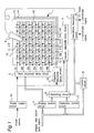
- Fig. 1 is a block diagram of a display-integrated type tablet device of the present embodiment.
- the display-integrated type tablet device is approximately composed of an active matrix type LCD panel (referred to merely as the "display panel” hereinafter) 1 which concurrently has an image display function and an electrostatic induction tablet function, a row electrode drive circuit 2 and a column electrode drive circuit 3 for driving the display panel 1, a display control circuit 4 for supplying a display control signal to the row electrode drive circuit 2 and the column electrode drive circuit 3, a detection control circuit 5 for supplying a detection control signal to the column electrode drive circuit 3, a coordinate detection circuit 7 for detecting the coordinates at the tip end of an electronic pen 6 on the display panel 1 by receiving a signal from the electronic pen 6, and a control circuit 9 for controlling a switching circuit 8 and the coordinate detection circuit 7 to execute an image display operation and a coordinate detection operation.
- an active matrix type LCD panel referred to merely as the "display panel” hereinafter
- the display panel 1 has a plurality of row electrodes G1, G2, G3, ..., G6 (an arbitrary row electrode referred to as G hereinafter) arranged in parallel on a transparent TFT (Thin Film Transistor) substrate 10 and a plurality of column electrodes S1, S2, S3, ..., S6 (an arbitrary column electrode referred to as S hereinafter) which are arranged in parallel and cross the row electrodes G at right angles.
- a TFT 11 In a position where each row electrode G and each column electrode S cross each other is provided a TFT 11.
- Each TFT 11 has a gate electrode connected to the row electrode G and a source electrode connected to the column electrode S.
- the TFT 11 has a drain electrode connected to a pixel electrode 12.
- Pixel electrodes 12 are arranged in a matrix form in an area surrounded by each row electrode G and each column electrode S.
- an opposite substrate 13 On the rear side of the TFT substrate 10 is provided an opposite substrate 13 arranged opposite to the TFT substrate 10. On an inner surface of the opposite substrate 13 is provided an opposite electrode 14 having approximately same area as that of the TFT substrate 10. Between the pixel electrodes 12 and the opposite electrode 14 is interposed liquid crystals (not shown) to constitute a pixel matrix.
- the row electrode drive circuit 2 successively applies scanning pulses of row electrode scanning signals g1 through g6 (an arbitrary row electrode scanning signal referred to as g hereinafter) to respective row electrodes G on the display panel 1 to scan the row electrodes G. Then the scanning pulses are applied to the gate electrode of each TFT 11 by way of the row electrode G to turn on the TFT 11.
- row electrode scanning signals g1 through g6 an arbitrary row electrode scanning signal referred to as g hereinafter
- the column electrode drive circuit 3 applies to each column electrode S column electrode drive signals s 1 1 through s 1 6 (an arbitrary column electrode drive signal referred to as s 1 hereinafter) having drive pulses corresponding to the contents of an image to be displayed relevant to each row electrode G in synchronization with the scanning of the row electrode G. Then the drive pulses are applied to the source electrode of the TFT 11 by way of the column electrode S, with which the signal voltage is applied to the pixel electrode 12 connected to the drain electrode of the TFT 11 which has been turned on by the scanning of the row electrode G by the row electrode drive circuit 2. Thus the image is written into the pixel corresponding to the contents of image display.
- the column electrode drive circuit 3 successively applies scanning pulses of column electrode scanning signals s 2 1 through s 2 6 (an arbitrary column electrode scanning signal referred to as s 2 hereinafter) to respective column electrodes S independently of the scanning of the row electrodes G to scan the column electrode S.
- the scanning pulses generated by the row electrode drive circuit 2 and the drive pulses and scanning pulses generated by the column electrode drive circuit 3 are generated by a bias voltage from the power supply circuit 16.
- the display control circuit 4 generates a display control signal for displaying an image on the display panel 1 based on display data and sync signals input from outside of the circuit. Then the generated display control signal is transmitted to the row electrode drive circuit 2 to control the operation of the row electrode drive circuit 2. Furthermore, the display control signal and the input display data signal are transmitted to the switching circuit 8. Meanwhile, the detection control circuit 5 generates a detection control signal for detection of the coordinates at the tip end of the electronic pen 6 based on the sync signals and transmits the signal to the switching circuit 8.
- the switching circuit 8 switchingly selects the display control signal and the display data from the display control circuit 4, or the detection control signal from the detection control circuit 5 and transmits the same to the column electrode drive circuit 3.
- the operation of the column electrode drive circuit 3 is controlled by the display control signal or the detection control signal.
- the electronic pen 6 has a high- input - impedance detection electrode (not shown) coupled with the row electrode G and the column electrode S of the display panel 1 through a stray capacitance. Therefore, an induction voltage is induced at the detection electrode due to the scanning pulses applied to the row electrode G or the scanning pulses applied to the column electrode S.
- the coordinate detection circuit 7 detects the generation timing of the induction voltage generated at the detection electrode of the electronic pen 6 based on a coordinate detection timing signal from the control circuit 9 to detect the coordinates at the tip end of the electronic pen 6.
- Figs. 2A and 2B show a relation in position between the display panel 1 and the electronic pen 6, where Fig. 2A is a perspective front view and Fig. 2B is a sectional view.
- the electronic pen 6 is positioned on the side of the TFT substrate 10 of the display panel 1 and its detection electrode i.e. tip electrode is coupled with the row electrode G and the column electrode S on the TFT substrate 10 through a stray capacitance.
- the electronic pen 6 is positioned on the side of the TFT substrate 10 opposite from a back light 17 with the opposite electrode 14, high-frequency noise from the back light 17 is intercepted by the opposite electrode 14 to prevent the noise from the back light 17 from being superimposed on the induction voltage induced at the tip electrode of the electronic pen 6.
- the electrostatic coupling between the tip electrode of the electronic pen 6 and the row electrode G and the column electrode S is shielded by the opposite electrode 14 to produce the effect of preventing the induction voltage induced at the tip electrode of the electronic pen 6 from being reduced.
- the coordinates at the tip end of the electronic pen 6 on the display panel 1 can be stably detected with high accuracy.
- an x-coordinate signal and a y-coordinate signal representing the coordinates at the tip end are output from the coordinate detection circuit 7. Then, based on the x-coordinate signal and the y-coordinate signal, the display data for displaying a dot image in a position at the tip end of the electronic pen 6 on the display panel 1 is generated by display data signal generation means (not shown because it has no direct relation with the present embodiment), and then input to the display control circuit 4 in a manner as described hereinbefore.
- a letter or a figure can be written into the display panel 1 by means of the electronic pen 6 as if the letter or figure were written on a paper with writing implements.
- recognition means (not shown) from a change in the x-coordinate signal and the y-coordinate signal, and therefore the result of recognition can be used to execute document formation, designation of control, and the like.
- the result of recognition can be also used as response means for icons displayed on the display panel 1.
- Fig. 3 is a chart showing the operation timing of the aforementioned display-integrated type tablet device.
- One cycle Tv of a vertical sync signal V is divided into an image display period (y-coordinate detection period) T1 and an x-coordinate detection period T2 of one frame, where the x-coordinate detection period T2 is equal to a vertical blanking period Tb.
- the division into the detection period (y-coordinate detection period) T1 and the x-coordinate detection period T2 is executed by switchingly selecting between the display control circuit 4 and the detection control circuit 5 by means of the switching circuit 8.
- the display control circuit 4 is switchedly selected by the switching circuit 8 based on a switching signal from the control circuit 9, and the row electrode drive circuit 2 and the column electrode drive circuit 3 are controlled by a display control signal from the display control circuit 4. Then the row electrode scanning signal g is output from the row electrode drive circuit 2 to scan or select a row electrode G on the display panel 1. Meanwhile, the column electrode drive signal s 1 corresponding to the display data signal is output from the column electrode drive circuit 3 to be applied to the column electrode S. Thus the image of one frame is displayed on the display panel 1.
- the detection control circuit 5 is switchedly selected by the switching circuit 8, and the column electrode drive circuit 3 is controlled by a detection control signal from the detection control circuit 5. Then the column electrode scanning signal s 2 is output from the column electrode drive circuit 3 to scan the column electrode S of the display panel 1.
- the x-coordinate at the tip end of the detection pen 6 is detected by detecting the application timing of the scanning pulse successively applied to the column electrode S on the display panel 1 by the column electrode drive circuit 3 by means of the tip electrode of the detection pen 6 in the x-coordinate detection period T2. Meanwhile, the y-coordinate at the tip end of the detection pen 6 is detected by detecting the application timing of the scanning pulse successively applied to the row electrode G by the row electrode drive circuit 2 by means of the tip electrode of the detection pen 6 in the image display period (y-coordinate detection period) T1.
- the row electrode scanning pulse for image display concurrently serves as the row electrode scanning pulse for coordinate detection.
- the entire vertical blanking period Tb can be assigned to the x-coordinate detection period to prevent the electrode scanning speed from increasing and allow the x-coordinate detection accuracy to be increased. Since the y-coordinate detection is executed in the image display period T1 that is longer than the vertical blanking period Tb, the y-coordinate detection accuracy can be also increased.
- Fig. 4 is a timing chart of a variety of signals in the operation of the aforementioned display-integrated type tablet device. The following describes in detail the operation of the display-integrated type tablet device with reference to Fig. 4.
- the sync signals input to the display control circuit 4, detection control circuit 5, and control circuit 9 include a horizontal sync signal H as well as the vertical sync signal V.
- the vertical sync signal V has a cycle corresponding to one image frame display period, while the horizontal sync signal H has a cycle corresponding to one horizontal image scan period.
- eight cycles of the horizontal sync signal H correspond to one cycle of the vertical sync signal V.
- the row electrode drive circuit 2 successively applies the scanning pulse of the row electrode scanning signal g to the row electrode G in synchronization with one cycle of the horizontal sync signal H in the image display period (y-coordinate detection period) T1 in a manner as described above.
- the scanning pulse successively applied to the row electrode G is used as the scanning pulse for image display and the scanning pulse for y-coordinate detection.
- the column electrode drive circuit 3 operates in synchronization with each cycle of the horizontal sync signal H in the image display period (y-coordinate detection period) T1 in the same manner as in the normal active matrix type LCD panel as described hereinbefore to output to all the column electrodes S the column electrode drive signal s 1 into which drive pulses corresponding to the display data are inserted. It should be noted that the drive pulses are not shown in Fig. 4.
- a scanning pulse of the column electrode scanning signal s 2 is successively applied to three column electrodes S every one cycle of the horizontal sync signal H to scan all the column electrodes S in two cycles of the horizontal sync signal H.
- the scanning pulse successively applied to the column electrode S is used as the scanning pulse for x-coordinate detection.
- a voltage at the opposite electrode 14 is made constant to adopt the arrangement of inverting in polarity the voltage applied to the pixel electrode 12 constituting each pixel of the pixel matrix with respect to the voltage at the opposite electrode 14.
- the level of a reference voltage of the column electrode drive signal s 1 output from the column electrode drive circuit 3 is inverted every frame.
- the electric potential level at the pixel electrodes 12 connected to an identical row electrode G via the TFT 11 is inverted every time the scanning pulse is applied to the row electrode G, with which the electric potential at each of the pixel electrodes 12 with respect to the electric potential at the opposite electrode 14 is inverted in polarity.
- the present embodiment is constructed by incorporating the detection control circuit 5, switching circuit 8, coordinate detection circuit 7, control circuit 9, and detection pen 6 to an active matrix type LCD panel approximately composed of the display panel 1, row electrode drive circuit 2, column electrode drive circuit 3, display control circuit 4, and power supply circuit 16. Then each frame period is time-sharingly divided into the image display period (y-coordinate detection period) T1 in which an image is displayed on the pixel matrix of the display panel 1 and the y-coordinate at the tip end of the electronic pen 6 on the display panel 1 is detected, and the x-coordinate detection period T2 in which the x-coordinate at the tip end of the electronic pen 6 on the display panel 1 is detected.
- the switching circuit 8 selects the display control circuit 4 under the control of the control circuit 9. Then the row electrodes G are sequentially scanned by the row electrode drive circuit 2 to be selected, while the column electrodes S are driven by the column electrode drive circuit 3 to display an image on the pixels relevant to the selected row electrode G according to the display data.
- the y-coordinate at the tip end of the electronic pen 6 is stably detected with high accuracy by the coordinate detection circuit 7 based on an induction voltage induced at the tip electrode of the electronic pen 6 due to the scanning pulses of the row electrode scanning signal g output from the row electrode drive circuit 2 to the row electrode G.
- the switching circuit 8 selects the detection control circuit 5 under the control of the control circuit 9. Then the scanning pulse of the column electrode scanning signal s 2 is successively applied to the column electrodes S of the display panel 1 by the column electrode drive circuit 3 to sequentially scan the column electrodes S. Then an induction voltage is induced at the tip end of the electronic pen 6, and the x-coordinate at the tip end of the electronic pen 6 is detected by the coordinate detection circuit 7 based on the induction voltage to consequently output an x-coordinate signal.
- the display panel 1 is made to function as a tablet integrated with an image display function.
- the present embodiment can concurrently solve all the problems of the reduction of brightness and contrast of the display screen in the image display section attributed to the low light transmittance of the row and column electrodes of the conventional tablet, the reduction of visibility of the display section attributed to the regularity in electrode arrangement of the tablet and a misalignment between the display section and the tablet section, and the increase in thickness as well as the increase in cost of the laminated body of the tablet and the display section.
- the display-integrated type tablet device of the present embodiment can achieve a display screen with high visibility in inputting a position on the display screen by means of the electronic pen while allowing reduction in thickness and cost of the device.
- the entire one frame period can be used as the coordinate detection period. Therefore, the coordinate detection speed can be reduced to allow the coordinates at the tip end of the display pen 6 to be stably detected with high accuracy.
- the above arrangement can cope with the increase in number of the row electrodes G and the column electrodes S in company with the increase in area of the display panel.
- the detection of the y-coordinate at the tip end of the electronic pen 6 is executed by utilizing the scanning pulses applied to the row electrode G in scanning the row electrodes in the image display period T1. Therefore, in detecting the y-coordinate, there is no need to apply to the row electrode G a specific scanning pulse which does not turn on the TFT 11. Furthermore, since the TFT 11 is in the off state in the x-coordinate detection stage, the electronic charges accumulated in the pixel electrode 12 do not change even when scanning pulse is applied to the column electrode S, which does not cause deterioration in image display quality.
- a display panel 1 having six row electrodes G and six column electrodes S for simplicity of explanation.
- a practical display panel 1 is provided with, for example, 480 row electrodes G and 640 column electrodes S.
- the display-integrated type tablet device shown in Figs. 1, 2A, 2B, 3, and 4 has the following problems, and therefore the present second embodiment is to solve the problems.
- an equivalent capacity composed of the pixel electrode 12, the opposite electrode 14, and the liquid crystals interposed between the pixel electrode 12 and the opposite electrode 14 of the display pixel on the pixel matrix is electrically charged to display an image on the display pixel.
- the rise time and the fall time of the scanning pulses to be applied to adjoining row electrodes G are placed very close to each other.
- the trailing edge of a scanning pulse applied to a row electrode G suppresses the leading edge of the scanning pulse applied to the next row electrode G to suppress the change of an induction voltage to be induced at the tip end of the electronic pen 6.
- the above fact results in the problem that such induction voltage that exhibits a remarkable peak when the row electrode G located at the tip end of the electronic pen 6 is scanned cannot be obtained.
- the display panel 1 is driven by an alternating voltage in order to prevent the possible deterioration of the liquid crystals.
- the level of the voltage of the column electrode drive signal s 1 successively applied from the column electrode drive circuit 3 to the column electrode S is inverted every frame (i.e., every one cycle of the vertical sync signal V) with respect to the voltage at the opposite electrode 14.
- the resulting display image flickers to deteriorate the image display quality.
- the y-coordinate detection accuracy can be increased by separating only the regular detection signal from the detection signal output from the electronic pen 6.
- the scanning pulse of the row electrode drive signal g has a pulse width set up very close to one cycle of the horizontal sync signal H, the generation timing of the scanning pulses of the row electrode drive signal g and the change timing of the voltage of the column electrode drive signal s 1 are placed very close to each other in the image display period. Therefore, it is not easy to separate apart both the pulses.
- the row electrode drive signal g of which voltage changes in synchronization with one cycle of the horizontal sync signal H as shown in Fig. 5 changes in a number of levels according to the contents of the display image (the change in level eliminated in Fig. 5). Therefore, the change in level of the voltage applied to the column electrodes S due to the change of the contents of the display image exerts not a little irregular influence on the detection signal output from the electronic pen 6. For the above reason, it is still more difficult to separate the regular detection signal and the noise from the detection signal output from the electronic pen 6 in scanning the row electrodes.
- the second embodiment provides an active matrix type display-integrated type tablet device capable of increasing the accuracy in detecting the coordinates at the tip end of the electronic pen in scanning the electrode connected to the control terminal of the switching element and a method for driving the device.
- the display-integrated type tablet device of the second embodiment has the same basic construction as that of the display-integrated type tablet device of the first embodiment shown in Fig. 1.
- the reference numerals shown in Fig. 1 are used at need, and no detailed description is provided for the constituent elements relevant to the used reference numerals.
- the present invention relates to the row electrode drive circuit 2 shown in Fig. 1, and reference is made mainly to the row electrode drive circuit 2 hereinafter.
- the second embodiment adopts in the image display period the arrangement of making the scanning pulse of the row electrode scanning signal g for turning on the TFT 11 for image display have a pulse width very close to one cycle of the horizontal sync signal H by scanning the row electrode G connected to the gate electrode of the TFT 11 with row electrode scanning signals g a , g b , g c , and g d having waveforms as shown in Fig.
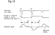
- Fig. 15 shows the waveform of a detection signal induced at the tip electrode of the electronic pen 6 due to the change of the voltage of the column electrode drive signal s 1 applied to the column electrode S in the image display period in synchronization with the horizontal sync signal H.
- the detection signal attributed to the change of the voltage of the column electrode drive signal s 1 exhibits its maximum value immediately after the change of the voltage. Then the signal gradually approaches the reference voltage to approximately reach the reference voltage at a time point (b), and thereafter the signal maintains its voltage level until the voltage of the column electrode drive signal s 1 changes subsequently.
- the detection signal maintains a stable state regardless of the change of the voltage of the column electrode drive signal s 1 .
- the application of the scanning pulse for coordinate detection to the row electrode G in the image display period should be idealistically so timed that the change of the voltage of the column electrode drive signal s 1 exerts no influence on the pulse application and the time of application is put apart from a time point (c) of the change of the voltage of the column electrode drive signal s 1 .
- the row electrode drive circuit 2 generates in the image display period row electrode scanning signals g a through g d in which a coordinate detection pulse PY is incorporated in a position corresponding to the elapse of the time "T 0 " from the fall time of the horizontal sync signal H to an image display pulse PT for turning on the TFT 11 (refer to Fig. 14).
- the time "T 0" is appropriately set up in consideration of the impedance of the column electrode S and the response speed of the tip electrode of the electronic pen 6.
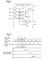
- Fig. 6 is a diagram of a part of a row electrode scanning signal generation section of the row electrode drive circuit 2 of the second embodiment
- Fig. 7 is a timing chart of a variety of signals input to or output from the row electrode scanning signal generation section.
- the row electrode scanning signal g a shown in Fig. 14 is generated.
- the row electrode scanning signal g a has a waveform in which a slit of the coordinate detection pulse PY is formed in accordance with the timing "T 0 " in the image display pulse PT of the conventional row electrode scanning signal g .
- one unit is composed of a shift register 21, inverters 52 and 23, and AND-gates 24, 25, 26, and 27.
- a shift data signal s generated in the display control circuit 4.
- a first clock signal ck1 obtained by inverting the horizontal sync signal H. Then the pulse of the shift data signal s is shifted in synchronization with the first clock signal ck1 and then output from output terminals Q1, Q2, Q3, and Q4.
- the inverter 52 To the inverter 52 is input the first clock signal ck1. Meanwhile, to the inverter 23 is input a second clock signal ck2 obtained by delaying in phase the first clock signal ck1 by the time "T 0 ".
- each of output signals from the output terminals Q2, Q3, and Q4 of the shift register 21, the output signal from the inverter 52, and the output signal from the inverter 23 are input to each of the AND-gates 25, 26, and 27.
- From the AND-gate 24 is output a row electrode scanning signal g a 1.
- each of row electrode scanning signals g a 2, g a 3, and g a 4 is output from each of the AND-gates 25, 26, and 27.
- the pulse of the shift data signal s is shifted in synchronization with the fall time of the first clock signal ck1 and then successively output via the AND-gates 24, 25, 26, and 27 to form the image display pulse PT in the row electrode scanning signals g a 1, g a 2, g a 3, and g a 4.
- the row electrode scanning signals g a 1, g a 2, g a 3, and g a 4 are at "L" level in the period in which the first clock signal ck1 is at "H” level and the output signal of the inverter 52 is at "L” level to correctly regulate the width of the image display pulse PT.
- the second clock signal ck2 is a signal for forming the coordinate detection pulse PY in the image display pulse PT set up in a manner as described above. Only in the period in which the second clock signal ck2 is at "H” level, the outputs of the AND-gates 24, 25, 26, and 27 are at "L” level. Thus the coordinate detection pulse PY is formed in a slit shape in the image display pulse PT. In the above case, since the second clock signal ck2 is a signal obtained by delaying in phase the first clock signal ck1 by the time "T 0 ", the coordinate detection pulse PY is formed in the position corresponding to the elapse of the time "T 0 " from the fall time of the horizontal sync signal H.
- the coordinate detection pulse PY can be formed in an idealistic position free from the influence of the change of the voltage of the column electrode drive signal s 1 where the pulse is separated in time apart from the time point of change of the reference voltage of the column electrode drive signal s 1 .
- the y-coordinates at the tip end of the electronic pen 6 is detected by the coordinate detection circuit 7.
- a gate 701 provided in the coordinate detection circuit 7 extracts the detection signal from the electronic pen 6 only in a period "E" set up so as to include the period in which the coordinate detection pulse PY is generated within the period in which the image display pulse PT is generated in a manner as shown in Fig. 14.
- the image display pulse PT of the row electrode scanning signal is generated by the shift register 21, and the coordinate detection pulse PY is formed in the position corresponding to the elapse of the time "T 0 " from the fall time of the horizontal sync signal H by the inverter 23 and the AND-gates 24, 25, 26, and 27 to generate the row electrode scanning signal g a in which the coordinate detection pulse PY is formed in a slit shape in the image display pulse PT.
- noise based on the column electrode drive signal s 1 applied to the column electrode S is not superimposed on the voltage induced at the tip electrode of the electronic pen 6 due to the coordinate detection pulse PY applied to the row electrode G of the display panel 1 to allow the y-coordinate at the tip end of the electronic pen 6 to be detected with high accuracy.
- the coordinate detection pulse PY is formed in a slit shape in the image display pulse PT of the row electrode scanning signal g a , the time required for electrically charging the pixel electrode 12 is reduced by the time corresponding to the slit-shaped pulse. Therefore, it is required to set up the pulse width of the image display pulse PT so that a sufficient time can be assured for the above-mentioned charging time.
- the present third embodiment relates to generation of a row electrode scanning signal g b shown in Fig. 14.
- Fig. 8 is a diagram showing a part of a row electrode scanning signal generation section of a row electrode drive circuit 2
- Fig. 9 is a timing chart of a variety of signals input to and output from the row electrode scanning signal generation section.
- the same reference numerals as in Fig. 6 are given to the same constituent elements as the constituent elements shown in Fig. 6.
- the row electrode scanning signal g b generated in the present third embodiment has a waveform in which a coordinate detection pulse PY generated in accordance with the timing "T 0 " is formed independently of the image display pulse PT.
- one unit is composed of a first shift register 21, a second shift register 21', an inverter 52, AND-gates 24, 25, 26, 27, 24', 25', 26', and 27', and OR-gates 28, 29, 30, and 31.
- the first shift register 21, the inverter 52, and the AND-gates 24, 25, 26, and 27 operate in the same manner as in the second embodiment based on the first shift data signal s1 and the first clock signal ck1 (signal obtained by inverting the horizontal sync signal H) from the display control circuit 4 to form an image display pulse PT of the row electrode scanning signal g b as shown in Fig. 9.
- the second shift register 21' and the AND-gates 24', 25', 26', and 27' form a coordinate detection pulse PY independently of the image display pulse PT based on a second shift data signal s2 and a second clock signal ck2 in a manner as follows.
- the second clock signal ck2 is a signal obtained by delaying in phase the first clock signal ck1 by the aforementioned time “T 0 ". Therefore, the pulse of the second shift data signal s2 is shifted in synchronization with the second clock signal ck2 to be successively output from output terminals Q1 through Q4 of the second shift register 21' at a time delayed by the time "T 0 " from the rise time of the first clock signal ck1.
- the signal output from the output terminals Q1 through Q4 of the second shift register 21' and the second clock signal ck2 are input to the AND-gates 24', 25', 26', and 27'. Then the AND-gates 24', 25', 26', and 27' output a pulse signal (coordinate detection pulse PY) obtained by cutting the output signal from the second shift register 21' at the rise time and the fall time of the second clock signal ck2.
- the image display pulse PT output from the AND-gate 24 and the coordinate detection pulse PY output from the AND-gate 24' are input to the OR-gate 28.
- the image display pulses PT output from the respective AND-gates 25, 26, and 27 and the respective coordinate detection pulses PY output from the respective AND-gates 25', 26', and 27' are input respectively to the OR-gates 29, 30, and 31.
- the OR-gates 29, 30, and 31 output the row electrode scanning signal g b having the image display pulse PT and the coordinate detection pulse PY which are formed independently of each other as shown in Fig. 9.
- the coordinate detection pulse PY is formed in a position corresponding to the elapse of the time "T 0 " from the fall time of the horizontal sync signal H.
- the coordinate detection pulse PY can be formed in an idealistic position free from the influence of the change of the voltage of the column electrode drive signal s 1 where the pulse is separated in time apart from the time point of change of the voltage of the column electrode drive signal s 1 .
- the y-coordinates at the tip end of the electronic pen 6 is detected.
- the y-coordinate detection can be executed without being influenced by the rise time and the fall time of the image display pulse PT.
- the coordinate detection pulse PY is formed immediately before the image display pulse PT as shown in Fig. 9. With the above-mentioned arrangement, the image once written into the unintended pixel is immediately erased with application of the next image display pulse PT to result in causing no problem.
- the present fourth embodiment relates to generation of a row electrode scanning signal g c shown in Fig. 14.
- Fig. 10 is a diagram showing a part of a row electrode scanning signal generation section of a row electrode drive circuit 2 of the present fourth embodiment, while Fig. 11 is a timing chart of a variety of signals input to and output from the row electrode scanning signal generation section.
- Fig. 8 the same reference numerals as in Fig. 8 are given to the same constituent elements as the constituent elements shown in Fig. 8.
- the row electrode scanning signal g c generated in the present fourth embodiment has a waveform in which a coordinate detection pulse PY generated in accordance with the timing "T 0 " is formed continuously with an image display pulse PT.
- one unit is composed a first shift register 21, a second shift register 21', an inverter 52, AND-gates 24, 25, 26, and 27, and OR-gates 28, 29, 30, and 31.
- the row electrode scanning signal g c of the present fourth embodiment is different from the row electrode scanning signal g b generated in the third embodiment in the point that a coordinate detection pulse PY is not cut off at the fall time of the second clock signal ck2.
- the fourth embodiment has a construction in which the AND-gates 24', 25', 26', and 27' for cutting off the coordinate detection pulse PY at the fall time of the second clock signal ck2 are removed from the row electrode scanning signal generation section of the third embodiment in Fig. 8.
- the first shift register 21, the inverter 52, and the AND-gates 24, 25, 26, and 27 operate in the same manner as in the third embodiment to form a image display pulse PT of the row electrode scanning signal g c based on the first shift data signal s1 and the first clock signal ck1 from the display control circuit 4.
- the second shift register 21' shifts the pulse of the second shift data signal s2 in synchronization with the second clock signal ck2 obtained by delaying in phase the first clock signal ck1 by the aforementioned time "T 0 " and successively outputs the pulse as a coordinate detection pulse PY.
- the image display pulse PT output from the AND-gate 24 and the coordinate detection pulse PY output from the output terminal Q1 of the second shift register 21' are input to the OR-gate 28.
- respective image display pulse PT output from the AND-gates 25, 26, and 27 and respective coordinate detection pulse PY output from the output terminals Q2, Q3, and Q4 of the second shift register 21' are input respectively to the OR-gates 29, 30, and 31.
- the OR-gates 28, 29, 30, and 31 output the row electrode scanning signal g c having the image display pulse PT and the coordinate detection pulse PY which are formed continuously (the image display pulse PT and the coordinate detection pulse PY formed continuously referred to collectively as a "scanning pulse” hereinafter) as shown in Fig. 11.
- the coordinate detection pulse PY can be formed in an idealistic position free from the influence of the change of the voltage of the column electrode drive signal s 1 where the pulse is separated in time apart from the time point of change of the voltage of the column electrode drive signal s 1 .
- the y-coordinate detection can be executed without being influenced by the fall time of the image display pulse PT.
- the present fifth embodiment relates to generation of a row electrode scanning signal g d shown in Fig. 14.
- Fig. 12 is a diagram showing a part of a row electrode scanning signal generation section of a row electrode drive circuit 2 of the present fifth embodiment
- Fig. 13 is a timing chart of a variety of signals input to and output from the row electrode scanning signal generation section.
- the same reference numerals as in Fig. 10 are given to the same constituent elements as the constituent elements shown in Fig. 10.
- the row electrode scanning signal g d generated in the present fifth embodiment has a waveform in which a coordinate detection pulse PY generated in accordance with the timing "T 0 " and an image display pulse PT are formed continuously in the same manner as in the fourth embodiment.
- the shift data signal s1 for generating the coordinate detection pulse PY and the shift data signal s2 for generating the image display pulse PT are different shift data signals, where the coordinate detection pulse PY is formed so as to elongate the width of the image display pulse PT.
- the coordinate detection pulse PY and the image display pulse PT are generated based on an identical shift data signal s to form the coordinate detection pulse PY so as to shorten the width of the image display pulse PT.
- one unit is composed of a shift register 21, an inverter 52, AND-gates 24, 25, 26, 27, 32, 33, 34, and 35, and a flip-flop 36.
- the shift register 21, the inverter 52, and the AND-gates 24, 25, 26, and 27 form an image display pulse PT of a row electrode scanning signal g d based on the shift data signal s and the first clock signal ck1 from the display control circuit 4.
- the flip-flop 36 is an SR flip-flop in which, when the level of the first clock signal ck1 input to its set input terminal S becomes “H", a signal at "L” level is output from its output terminal Q until the level of the second clock signal ck2 input to its reset terminal R becomes "H".
- the image display pulses PT output from the AND-gates 24, 25, 26, and 27 are input respectively to the AND-gates 32, 33, 34, and 35.
- the signal output from the output terminal Q of the flip-flop 36 is input to each of the AND-gates 32, 33, 34, and 35.
- a fore portion of the image display pulse PT is cut off by the output signal from the flip-flop 36 in a manner as shown in Fig. 13 to consequently form the row electrode scanning signal g d in which the coordinate detection pulse PY and the image display pulse PT are formed continuously (the image display pulse PT and the coordinate detection pulse PY formed continuously referred to collectively as the "scanning pulse” hereinafter).
- the second clock signal ck2 input to the reset terminal R of the flip-flop 36 is a signal obtained by delaying in phase the first clock signal ck1 by the aforementioned time "T 0 ". Therefore, the coordinate detection pulse PY can be formed in an idealistic position free from the influence of the change of the voltage of the column electrode drive signal s 1 where the pulse is separated in time apart from the time point of change of the voltage of the column electrode drive signal s 1 .
- the y-coordinate detection can be executed without being influenced by the fall time of the image display pulse PT.
- the row electrode scanning signal generation section of the row electrode drive circuit 2 generates the row electrode scanning signal g a in which the coordinate detection pulse PY is inserted in the image display pulse PT, the row electrode scanning signal g b in which the image display pulse PT and the coordinate detection pulse PY are formed independently of each other, the row electrode scanning signal g c in which the coordinate detection pulse PY and the image display pulse PT are continuously formed in the row electrode scanning signal g b , or the row electrode scanning signal g d in which the fore portion of the image display pulse PT is cut before the coordinate detection pulse PY in the row electrode scanning signal g a .
- the rise time or the fall time of the coordinate detection pulse PY is set up at a time after the elapse of the time "T 0 " from the fall time of the horizontal sync signal H. Therefore, the coordinate detection pulse PY can be formed in an idealistic position free from the influence of the change of the voltage of the column electrode drive signal s 1 where the pulse is separated in time apart from the time point of change of the voltage of the column electrode drive signal s 1 .
- each of the aforementioned embodiments can be simply formed without incorporating any special circuit to the corresponding conventional circuit. Therefore, by implementing each row electrode drive circuit and the like by a semiconductor integrated circuit, further cost reduction and compacting can be achieved in comparison with the conventional display-integrated type tablet device.
- a display panel 1 having six row electrodes G and six column electrodes S for simplicity of explanation.
- a practical display panel 1 is provided with, for example, 480 row electrodes G and 640 column electrodes S.
- the row electrode scanning signal generation section of the row electrode drive circuit 2 has been described with regard to only one constituent unit thereof.
- a practical row electrode scanning signal generation section includes a specified number of the above-mentioned one unit formed in parallel corresponding to the number of the row electrodes G.
- the circuit construction of the row electrode scanning signal generation section of the present invention is not limited to the circuit construction of any of the aforementioned embodiments.
- the circuit construction is essentially required to be a circuit construction capable of generating the row electrode scanning signal having any of waveforms as shown in Fig. 14.
- the opposite electrode drive signal has been described as a constant DC level.
- the present invention can be also applied to a case where the opposite electrode is driven by an opposite electrode drive signal such that it changes in level in synchronization with the change of the voltage of the column electrode drive signal i.e., in the case where the electrode is driven in so-called the AC-driven manner.
- it is required to set up a detection pulse for the row electrode scanning signal so that the signal does not receive influence of the column electrode drive signal and the opposite electrode drive signal.
- the display-integrated type tablet device of an embodiment is constructed by incorporating the first position detection means for detecting the first position data representing the input position of the input pen means in the electro-optical material drive period in which an image is written into the electro-optical material and the second position detection means for detecting the second position data representing the input position in a period other than the electro-optical material drive period into a display-integrated type tablet device having the pair of transparent substrates with interposition of the electro-optical material, the pixel electrodes which are provided on one of the transparent substrates and connected to the switching elements, first and second electrode drive means for driving the first electrodes and the second electrodes connected to each of the switching elements, and input pen means electrostatically coupled with the first and second electrodes. Therefore, it is not required to set up any detection period for detecting the first position data of the input position pointed by the input pen means particularly in a period other than the electro-optical material drive period.
- the electro-optical material drive period is allowed to have a sufficient duration to allow the display screen to be easily increased in dimensions. Furthermore, the detection speed in detecting the position data can be set up at a slow speed to allow the accuracy in detecting the position data to be increased. Furthermore, the first electrode drive means is not required to generate any special signal for driving the first electrodes, which allows simplification of the first electrode drive means and high productivity to allow cost reduction to be achieved.
- the first electrodes are composed of row electrodes
- the second electrodes are composed of column electrodes
- the first electrode drive means is composed of row electrode drive means
- the second electrode drive means is composed of column electrode drive means.
- the position data of the input position pointed by the input pen means can be detected easily and securely.
- the row electrodes of the active matrix type display panel are sequentially scanned to be selected based on the row electrode scanning signal generated by the row electrode drive circuit according to a signal from the display control circuit, and an image is displayed on the pixel relevant to the selected row electrode according to display data based on the column electrode drive signal generated by the column electrode drive circuit.
- the y-coordinate at the tip end of the electronic pen is detected by the coordinate detection circuit based on a voltage induced at the electrode of the electronic pen due to the row electrode scanning signal applied to the row electrodes of the display panel.
- the column electrodes of the display panel are sequentially scanned based on the column electrode scanning signal generated by the column electrode drive circuit according to a signal from the detection control circuit, and the x-coordinate at the tip end of the electronic pen is detected by the coordinate detection circuit based on a voltage induced at the electrode of the electronic pen due to the column electrode scanning signal applied to the column electrodes.
- the coordinate detection operation can be executed stably and securely even when the row electrodes and the column electrodes are increased in number in company with the increase in area of the display panel to consequently allow an active matrix type display-integrated type tablet device which can be increased in area and has a high coordinate detection accuracy to be provided.
- the electro-optical material is implemented by liquid crystals, which allows cost reduction by utilizing an active matrix type LCD panel used normally.
- the first and second electrodes are driven by the first and second electrode drive means to selectively operate the switching elements connected to a plurality of pixel electrodes arranged in a matrix form to consequently write an image into the electro-optical material, the first position data representing the input position pointed by the input pen means in the electro-optical material drive period in which the image is written into the electro-optical material is detected, and the second position data representing the input position in the period other than the electro-optical material drive period is detected. Therefore, it is not required to set up any detection period for detecting the first position data of the input position pointed by the input pen means in the period other than the electro-optical material drive period.
- the first electrodes are composed of row electrodes
- the second electrodes are composed of column electrodes
- the first electrode drive means is composed of row electrode drive means
- the second electrode drive means is composed of column electrode drive means.
- the row electrode scanning signal is successively input to the row electrodes of the display panel to scan the row electrodes, while the column electrode drive signal is input to the column electrodes of the display panel to write an image into the electro-optical material.
- the y-coordinate at the tip end of the electronic pen is detected based on a voltage induced at the electrode of the electronic pen electrostatically coupled with the row electrodes due to the row electrode scanning signal applied to the row electrodes.
- the column electrode scanning signal is successively input to the column electrodes of the display panel to scan the column electrodes and the x-coordinate at the tip end of the electronic pen is detected based on a voltage induced at the electrode of the electronic pen due to the column electrode scanning signal input to the column electrodes. Therefore, the row electrode scanning speed and the column electrode scanning speed can be reduced.
- the coordinate detection operation can be executed stably and securely even when the row electrodes and the column electrodes are increased in number in company with the increase in area of the display panel to allow the coordinate detection accuracy to be increased.
- the present invention it is neither required to generate any special scanning pulse such that it does not turn on the switching element in scanning the row electrodes nor required to provide any pixel electrode for coordinate detection.
- the above arrangement allows a high-productivity low-cost display-integrated type tablet device utilizing the normal active matrix type LCD display device to be achieved.
- the electro-optical material is implemented by liquid crystals.
- the above arrangement allows a low-cost display-integrated type tablet device capable of detecting the first position data representing the input position pointed by the input pen means in the electro-optical material drive period to be easily achieved.
- the display-integrated type tablet device including a pair of transparent substrates having an electro-optical material interposed therebetween, pixel electrodes which are provided on one of the transparent substrates and connected to switching elements, first and second electrode drive means for driving first electrodes and second electrodes each connected to the switching elements, input pen means electrostatically coupled with the first and second electrodes, first position detection means for detecting the first position data representing the input position pointed by the input pen means in the electro-optical material drive period in which an image is written into the electro-optical material, and the second position detection means for detecting the second position data representing the input position in a period other than the electro-optical material drive period, the first electrode drive means is constructed so as to output a drive signal including a position data detection signal and an image display signal in driving the first electrodes. Therefore, the position data detection signal can be set up so that the signal can detect the position data without receiving noise attributed to the image display signal in detecting the first position data or noise in driving the second electrode
- the position data detection signal of the drive signal output from the first electrode drive means in detecting the first position data representing the input position pointed by the input pen means in the electro-optical material drive period is generated in the specified time different from the time when the induction voltage is generated in the input pen means in driving the second electrodes by the second electrode drive means in the electro-optical material drive period. Therefore, neither noise attributed to the image display signal nor noise in driving the second electrodes in the period other than the electro-optical material drive period is superimposed on the signal from the input pen means in detecting the first position data.
- the first position data representing the input position pointed by the input pen means can be detected with high accuracy.
- the signal output from the input pen means in a specified period including the rise time or the fall time of the position data detection signal is extracted, and based on the extracted signal, the first position data detection is executed. Therefore, only the above-mentioned signal from the input pen means attributed to the position data detection signal in the time when the first electrodes are driven is used to detect the first position data with high accuracy.
- the y-coordinate in detecting the y-coordinate at the tip end of the electronic pen, is detected based on the voltage of the coordinate detection pulse of the row electrode drive signal which is output from the row electrode drive circuit and includes the coordinate detection pulse for inducing an induction voltage at the electrode of the electronic pen in a specified time different from the generation time of the induction voltage induced at the electrode of the electronic pen due to the column electrode drive signal applied to the column electrodes and an image display pulse for applying a voltage to the control terminal of each of the switching elements of the display panel.
- the y-coordinate at the tip end of the electronic pen can be detected with high accuracy based on the signal different from the image display pulse of the row electrode drive signal without being influenced by the noise based on the image display signal and the column electrode drive signal.
- the row electrode scanning signal successively input to the row electrodes in scanning the row electrodes of the display panel is a row electrode scanning signal including the coordinate detection pulse for inducing an induction voltage at the electrode of the electronic pen in the specified time different from the generation time of an induction voltage induced at the electrode of the electronic pen due to the column electrode drive signal applied to the column electrodes and the image display pulse for applying a voltage to the control terminal of each of the switching elements of the display panel. Therefore, the noise based on the column electrode drive signal is not superimposed on the voltage induced at the electrode of the electronic pen in the time when the coordinate detection pulse of the row electrode scanning signal is applied to the row electrodes.
- the accuracy in detecting the coordinates at the tip end of the electronic pen in scanning the row electrodes connected to the control terminal of each of the switching elements can be increased.
Landscapes
- Engineering & Computer Science (AREA)
- General Engineering & Computer Science (AREA)
- Theoretical Computer Science (AREA)
- Human Computer Interaction (AREA)
- Physics & Mathematics (AREA)
- General Physics & Mathematics (AREA)
- Position Input By Displaying (AREA)
Claims (24)
- Eingabetablett mit integrierter Anzeige mit: einem Paar transparenter Substrate (10, 13), die einander gegenüberstehend angeordnet sind; einem elektrooptischen Material, das zwischen den Substraten angeordnet ist; einer Vielzahl von Pixelelektroden (12), die in einer Matrix auf einem (10) der transparenten Substrate angeordnet sind; einer Vielzahl von Schaltelementen (11), die jeweils mit einer zugehörigen der Pixelelektroden (12) verbunden sind; einer Vielzahl erster Elektroden (G) und zweiter Elektroden (S), wobei jedes der Schaltelemente (11) mit einer jeweiligen ersten Elektrode und einer jeweiligen zweiten Elektrode verbunden ist; einer ersten Elektrodenansteuerungseinrichtung (2) und einer zweiten Elektrodenansteuerungseinrichtung (3) zum Ansteuern der ersten bzw. zweiten Elektroden (G, S); einer Eingabegriffeleinrichtung (6), die elektrostatisch mit den ersten und zweiten Elektroden (G, S) gekoppelt ist; einer ersten Positionserfasssungseinrichtung (7) zum Erfassen erster Positionsdaten, die eine durch die Eingabegriffeleinrichtung (6) definierte Eingabeposition auf Grundlage eines Signals von der Eingabegriffeleinrichtung (6) repräsentieren; und einer zweiten Positionserfassungseinrichtung (7) zum Erfassen zweiter Positionsdaten, die eine Eingabeposition repräsentieren, die durch die Eingabegriffeleinrichtung (6) auf Grundlage eines Signals von dieser Eingabegriffeleinrichtung (6) in einer Zeit definiert ist, in der die zweiten Elektroden (S) durch die zweite Elektrodenansteuerungseinrichtung (3) in einer Periode angesteuert werden, die eine andere als eine Ansteuerungsperiode für das elektrooptische Material ist;wobei die Vorrichtung dadurch gekennzeichnet ist, dass die erste Positionserfassungseinrichtung so ausgebildet ist, dass sie die ersten Positionsdaten erfasst, wenn die ersten Elektroden (6) in der Ansteuerungsperiode für das elektrooptische Material angesteuert werden, wobei die ersten und zweiten Elektroden (G, S) durch die erste und zweite Elektrodenansteuerungseinrichtung (2, 3) in der Ansteuerungsperiode für das elektrooptische Material angesteuert werden, um die Schaltelemente (11) selektiv zu betreiben, um ein Bild in das elektrooptische Material einzuschreiben.
- Eingabetablett mit integrierter Anzeige nach Anspruch 1, bei dem die ersten Elektroden Zeilenelektroden (G) sind, die zweiten Elektroden Spaltenelektroden (S), die erste Elektrodenansteuerungseinrichtung eine Zeilenelektroden-Ansteuerungseinrichtung (2) ist und die zweite Elektroden-Ansteuerungseinrichtung eine Spaltenelektroden-Ansteuerungseinrichtung (3) ist.
- Eingabetablett mit integrierter Anzeige nach Anspruch 2, bei dem die Zeilenelektroden (G) parallel auf dem ersten transparenten Substrat (10) angeordnet sind und die Vielzahl von Spaltenelektroden (S) die Zeilenelektroden (6) rechtwinkligen auf dem ersten transparenten Substrat (10) schneidet, wobei jedes Schaltelement (11) an einer Position angeordnet ist, an der entsprechende Zeilen- und Spaltenelektroden (G, S) einander auf dem ersten transparenten Substrat (10) schneiden, und wobei jedes Schaltelement einen mit der entsprechenden Zeilenelektrode (G) verbundenen Steueranschluss und einen mit der entsprechenden Spaltenelektroden (S) verbundenen Eingangsanschluss aufweist; wobei jede Pixelelektrode (12) auf dem ersten transparenten Substrat (10 angeordnet ist und mit dem Ausgangsanschluss eines zugeordneten Schaltelements (11) verbunden ist; wobei die Vorrichtung ferner eine Gegenelektrode (14) auf dem anderen Substrat (13) aufweist, die den Pixelelektroden (12) gegenüberstehend angeordnet ist; wobei die Griffeleinrichtung ein elektronischer Griffel (6) ist, der an seinem Vorderende eine Elektrode aufweist, die elektrostatisch mit den Zeilenelektroden (G) und den Spaltenelektroden (S) der Anzeigetafel (1) gekoppelt ist;wobei die Vorrichtung ferner eine Anzeigesteuerungsschaltung (4) aufweist, die ein Anzeigesteuerungssignal und Anzeigedaten zum Anzeigen eines Bilds in einer Pixelmatrix aus einer Fläche der Pixelelektroden (12) der Anzeigetafel (1) ausgibt;wobei die Vorrichtung ferner eine Erfassungssteuerungsschaltung (5) aufweist, die ein Abrastersteuerungssignal zum Abrastern der Spaltenelektroden der Anzeigetafel (1) aufweist;wobei die Vorrichtung ferner eine Schaltstufe (8) aufweist, die die Anzeigesteuerungsschaltung in einer Bildanzeigeperiode schaltend auswählt, um das Anzeigesteuerungssignal und die Anzeigedaten von der Anzeigesteuerungsschaltung auszugeben, und die die Erfassungssteuerungsschaltung (5) in einer x-Koordinatenerfassungsperiode schaltend auswählt, um das Abrastersteuersignal von der Erfassungssteuerschaltung (5) auszugeben;wobei die Zeilenelektroden-Ansteuerungsschaltung (2) so ausgebildet ist, dass sie in der Bildanzeigeperiode auf Grundlage des Anzeigesteuerungssignal von der Anzeigesteuerungsschaltung (4) ein Zeilenelektroden-Abrastersignal zum sequenziellen Abrastern der Zeilenelektroden (G) erzeugt;wobei die Spaltenelektroden-Ansteuerungsschaltung (3) so ausgebildet ist, dass sie ein Spaltenelektroden-Ansteuerungssignal erzeugt, um an die Elektroden (12), die mit den Zeilenelektroden (G) verbunden sind, die in der Bildanzeigeperiode abgerastert werden, elektrische Ladungen zum Anzeigen eines Bilds auf Grundlage des Anzeigesteuerungssignals und der Anzeigedaten von der Schaltstufe (8) zu liefern, und sie ein Spaltenelektroden-Abrastersignal zum sequenziellen Abrastern der Spaltenelektroden (S) in der x-Koordinatenerfassungsperiode auf Grundlage des Abrastersteuerungssignal von der Schaltstufe (8) erzeugt; undwobei die erste und die zweite Positionserfassungseinrichtung (7) so ausgebildet sind, dass sie die y-Koordinate am Vorderende des elektronischen Griffels (6) in der Bildanzeigeperiode auf Grundlage einer Spannung erfassen, die in der Elektrode des elektronischen Griffels (6) durch das Zeilenelektroden-Abrastersignal induziert wird, das von der Zeilenelektroden-Ansteuerungsschaltung (2) in jede der Zeilenelektroden eingegeben wird, und sie die x-Koordinate am Vorderende des elektronischen Griffels (6) in der x-Koordinatenerfassungsperiode auf Grundlage einer Spannung erfassen, die in der Elektrode des elektronischen Griffels (6) durch das Spaltenelektroden-Abrastersignal induziert wird, das von der Spaltenelektroden-Ansteuerungsschaltung (3) in jede der Spaltenelektroden (S) eingegeben wird.
- Eingabetablett mit integrierter Anzeige nach Anspruch 1, 2 oder 3, bei dem das elektrooptische Material ein Flüssigkristall ist.
- Verfahren zum Ansteuern eines Eingabetabletts mit integrierter Anzeige mit Folgendem: einem Paar transparenter Substrate (10, 13), die einander gegenüberstehend angeordnet sind; einem zwischen den Substraten angeordneten elektrooptischen Material, einer Vielzahl von Pixelelektroden (12), die in einer Matrix auf einem (10) der transparenten Substrate angeordnet sind; einer Vielzahl von Schaltelementen (11), die jeweils mit einer zugehörigen der Pixelelektroden (12) verbunden sind; einer Vielzahl erster Elektroden (G) und zweiter Elektroden (S), wobei jedes Schaltelement (11) mit einer jeweiligen ersten Elektrode und einer jeweiligen zweiten Elektrode verbunden ist; einer ersten Elektrodenansteuerungseinrichtung (2) und einer zweiten Elektrodenansteuerungseinrichtung (3) zum jeweiligen Ansteuern der ersten bzw. zweiten Elektroden (G, S) sowie einer Eingabegriffeleinrichtung (6), die elektrostatisch mit den ersten und zweiten Elektroden (G, S) gekoppelt ist; wobei das Verfahren die folgenden Schritte aufweist:wobei das Verfahren dadurch gekennzeichnet ist, dass es den Schritt des Erfassens der ersten Positionsdaten in einer Ansteuerungsperiode für das elektrooptische Material, in der ein Bild in das elektrooptische Material eingeschrieben wird, aufweist.Ansteuern der ersten und zweiten Elektroden (G, S) durch die erste und zweite Elektrodenansteuerungseinrichtung (2, 3) zum selektiven Betätigen der Schaltelemente (11), um dadurch ein Bild in das elektrooptische Material einzuschreiben;Erfassen erster Positionsdaten, die eine durch die Eingabegriffeleinrichtung (6) definierte Eingabeposition repräsentieren, auf Grundlage eines Signals von der Eingabegriffeleinrichtung (6), die elektrostatisch mit den ersten Elektroden (6) gekoppelt ist, innerhalb der Zeit, in der die ersten Elektroden (G) angesteuert werden; undErfassen zweiter Positionsdaten, die die durch die Eingabegriffeleinrichtung (6) definierte Eingabeposition repräsentieren, in einer anderen Periode als einer Ansteuerungsperiode für das elektrooptische Material auf Grundlage eines Signals von der Eingabegriffeleinrichtung (6), die elektrostatisch mit den zweiten Elektroden (S) gekoppelt ist, in einer Zeit, in der die zweiten Elektroden (S) durch die zweite Elektrodenansteuerungseinrichtung (3) angesteuert werden;
- Verfahren zum Ansteuern eines Eingabetabletts mit integrierter Anzeige nach Anspruch 5, bei dem die ersten Elektroden Zeilenelektroden (G) sind, die zweiten Elektroden Spaltenelektroden (S) sind, die ersten Elektrodenansteuerungseinrichtung eine Zeilenelektroden-Ansteuerungseinrichtung (2) ist und die zweite Elektrodenansteuerungseinrichtung eine Spaltenelektroden-Ansteuerungseinrichtung (3) ist.
- Verfahren zum Ansteuern eines Eingabetabletts mit integrierter Anzeige nach Anspruch 6, bei dem die Zeilenelektroden (G) parallel auf dem ersten Substrat (10) angeordnet sind und die Vielzahl von Spaltenelektroden (S) die Zeilenelektroden (G) rechtwinklig auf dem ersten transparenten Substrat (10) schneiden, wobei jedes Schaltelement (11) an einer Position angeordnet ist, an der zugeordnete Zeilen- und Spaltenelektroden (G, S) einander auf dem transparenten Substrat (10) schneiden, mit einem Steueranschluss, der mit der zugehörigen Zeilenelektrode (G) verbunden ist, und einem Eingangsanschluss, der mit der zugehörigen Spaltenelektrode (S) verbunden ist, wobei jede Pixelelektrode (12) mit einem Ausgangsanschluss eines zugehörigen Schaltelements (11) verbunden ist; wobei die Vorrichtung eine Gegenelektrode (14) auf dem anderen Substrat (13) aufweist, die den Pixelelektroden (12) gegenüberstehend angeordnet ist;
wobei die Griffeleinrichtung ein elektronischer Griffel (6) ist, der an seinem Vorderende eine Elektrode aufweist, die elektrostatisch mit den Zeilenelektroden (G) und den Spaltenelektroden (S) der Anzeigetafel (1) gekoppelt ist;wobei die Vorrichtung über eine Anzeigesteuerungsschaltung zum Ausgeben eines Anzeigesteuerungssignals sowie Anzeigedaten zum Anzeigen eines Bilds auf der Pixelmatrix aus einer Fläche der Pixelelektroden (12) der Anzeigetafel (1) aufweist;wobei die Vorrichtung eine Erfassungssteuerungsschaltung (5) zum Ausgeben eines Abrastersteuerungssignals zum Abrastern der Spaltenelektroden (S) der Anzeigetafel (1) aufweist;wobei die Vorrichtung eine Schaltstufe (8) zum schaltenden Auswählen der Anzeigesteuerungsschaltung (4) in einer Bildanzeigeperiode zum Ausgeben des Anzeigesteuerungssignals und der Anzeigedaten aus der Anzeigesteuerungsschaltung (4) sowie zum schaltenden Auswählen der Erfassungssteuerungsschaltung (5) in einer x-Koordinatenerfassungsperiode zum Ausgeben des Abrastersteuerungssignals von der Erfassungssteuerungsschaltung (5) aufweist;wobei die Zeilenelektroden-Ansteuerungsschaltung (2) so ausgebildet ist, dass sie ein Zeilenelektroden-Abrastersignal zum sequenziellen Abrastern der Zeilenelektroden (G) in der Bildanzeigeperiode auf Grundlage des Anzeigesteuerungssignals von der Anzeigesteuerungsschaltung (4) erzeugt; undwobei die Spaltenelektroden-Ansteuerungsschaltung (3) so ausgebildet ist, dass sie ein Spaltenelektroden-Ansteuerungssignal erzeugt, um an die Pixelelektroden (12), die mit den Zeilenelektroden (G) verbunden sind, die in der Bildanzeigeperiode auf Grundlage des Bildsteuerungssignals und der Anzeigedaten von der Schaltstufe (8) abgerastert werden, elektrische Ladungen zum Anzeigen eines Bilds zu liefern, und die ein Spaltenelektroden-Abrastersignal zum sequenziellen Abrastern der Spaltenelektroden (S) in der x-Koordinatenerfassungsperiode auf Grundlage des Abrastersteuerungssignals von der Schaltstufe (8) erzeugt, wobei das Verfahren die folgenden Schritte aufweist:aufeinanderfolgendes Eingeben des auf Grundlage des Anzeigesteuerungssignals erzeugten Zeilenelektroden-Abrastersignals in die Zeilenelektroden (6) der Aktivmatrix-Anzeigetafel (1) zum Abrastern der Zeilenelektroden (G), während das auf Grundlage des Anzeigesteuerungssignals erzeugte Spaltenelektroden-Abrastersignal und die Anzeigedaten aufeinanderfolgend in die Spaltenelektroden (S) der Anzeigetafel (1) eingegeben werden, um die Schaltelemente (11) selektiv anzusteuern, um dadurch ein Bild in das elektrooptische Material einzuschreiben;Erfassen einer y-Koordinate am Vorderende des elektronischen Griffels (6) in der Bildanzeigeperiode, in der das Bild in das elektrooptische Material eingeschrieben wird, auf Grundlage einer Spannung, die in der Elektrode des elektronischen Griffels (6) der elektrostatisch mit den Zeilenelektroden (G) gekoppelt ist, aufgrund des Zeilenelektroden-Abrastersignals induziert wird, wie es in jede der Zeilenelektroden (G) eingegeben wird;und Erfassen einer x-Koordinate am Vorderende des elektronischen Griffels (6) in der x-Koordinatenerfassungsperiode, die nicht die Bildanzeigeperiode ist, durch aufeinanderfolgendes Eingeben des auf Grundlage des Abrastersteuerungssignals erzeugten Spaltenelektroden-Abrastersignals in die Spaltenelektroden (S) der Anzeigetafel (1), um die Spaltenelektroden (S) durchzurastern, und auf Grundlage einer Spannung, die in der Elektrode des elektronischen Griffels (6) aufgrund des Spaltenelektroden-Abrastersignals induziert wird, das in jede der Spaltenelektroden (S) eingegeben wird. - Verfahren zum Ansteuern eines Eingabetabletts mit integrierter Anzeige nach Anspruch 5, 6 oder 7, bei dem das elektrooptische Material aus Flüssigkristallen besteht.
- Eingabetablett mit integrierter Anzeige nach Anspruch 1 oder 2, bei dem:die erste Elektroden-Ansteuerungseinrichtung (2) so ausgebildet ist, dass sie ein Ansteuerungssignal (ga, gb, gc, gd) ausgibt, das ein Positionsdaten-Erfassungssignal (PY) zum Erfassen der ersten Positionsdaten sowie ein Bildanzeigesignal (PT) zum Einschreiben eines Bilds in das elektrooptische Material beim Ansteuern der ersten Elektroden (G) beinhaltet.
- Eingabetablett mit integrierter Anzeige nach Anspruch 9, bei dem das Positionsdatenerfassungssignal (PY) im Ansteuerungssignal (ga, gb, gc, gd) von der ersten Elektroden-ansteuerungseinrichtung (2) innerhalb einer spezifizierten Zeit erzeugt wird, die sich von der Zeit unterscheidet, in der in der Elektrode der Eingabegriffeleinrichtung (6) eine Induktionsspannung in einer Zeit erzeugt wird, in der die zweiten Elektroden (S) durch die zweite Elektrodenansteuerungseinrichtung (3) innerhalb der Ansteuerungsperiode für das elektrooptische Material angesteuert werden.
- Eingabetablett mit integrierter Anzeige nach Anspruch 10, bei dem die erste Elektrodenansteuerungseinrichtung (2) mit einem Abschnitt (21) für sequenzielle Ausgabe, der das Bildanzeigesignal erzeugt und das Signal sequenziell ausgibt, und einem Gatterabschnitt (24, 25, 26, 27) versehen ist, der einen Teil des vom Abschnitt (21) für sequenzielle Ausgabe ausgegebenen Bildanzeigesignals für eine spezifizierte Periode unterbricht, um das Positionsdaten-Erfassungssignal (PY) in der spezifizierten Zeit zu erzeugen, um dadurch das Ansteuerungssignal (ga) zu erzeugen, in dem das Positionsdaten-Erfassungssignal (PY), das aus einem Schlitz mit spezifizierter Breite besteht, in das Bildanzeigesignal (PT) eingesetzt ist.
- Eingabetablett mit integrierter Anzeige nach Anspruch 10, bei dem die erste Elektrodenansteuerungseinrichtung (2) so ausgebildet ist, dass sie das Ansteuerungssignal (gb) so erzeugt, dass das Positionsdaten-Erfassungssignal (PY) vom Bildanzeigesignal (PT) getrennt ist.
- Eingabetablett mit integrierter Anzeige nach Anspruch 10, bei dem die erste Elektrodenansteuerungseinrichtung (2) so ausgebildet ist, dass sie das Ansteuerungssignal (gc) so erzeugt, dass das Positionsdaten-Erfassungssignal (PY) und das Bildanzeigesignal (PT) zueinander kontinuierlich verlaufen.
- Eingabetablett mit integrierter Anzeige nach Anspruch 9, bei dem die erste Elektrodenansteuerungseinrichtung (2) so realisiert ist, dass eine Erfassungsschaltung (24, 25, 26, 27, 23, 52; 21', 24', 25', 26', 27', 36) zum Erzeugen des Positionsdaten-Erfassungssignals (PY) mit einer Anzeigeschaltung (21) zum Erzeugen des Bildanzeigesignals (PT) in einer integrierten Halbleiterschaltung integriert ist.
- Eingabetablett mit integrierter Anzeige nach Anspruch 9, bei dem die erste Positionserfassungseinrichtung (7) innerhalb einer spezifizierten Periode, die einen Anstiegszeitpunkt oder einen Abfallzeitpunkt des Positionsdaten-Erfassungssignals (PY) beinhaltet, ein Signal von der Eingabegriffeleinrichtung (6) entnimmt, wenn sie die ersten Positionsdaten erfasst, die die Position der Eingabegriffeleinrichtung (6) in der Ansteuerungsperiode für das elektrooptische Material repräsentieren, und sie eine Erfassung der ersten Positionsdaten auf Grundlage des entnommenen Signals ausführt.
- Eingabetablett mit integrierter Anzeige nach Anspruch 2, bei dem die Elektroden (G) parallel auf dem ersten transparenten Substrat (10) angeordnet sind und die Vielzahl von Spaltenelektroden (S) die Zeilenelektroden (G) rechtwinklig auf dem ersten transparenten Substrat (10) schneiden und jedes der Schaltelement (11) an einer Position angeordnet ist, an der entsprechende Zeilen- und Spaltenelektroden (G, S) einander auf dem ersten transparenten Substrat (10) schneiden, wobei jedes Schaltelement einen mit der zugehörigen Zeilenelektrode (G) verbundenen Steueranschluss und einen mit der zugehörigen Spaltenelektrode (S) verbundenen Eingangsanschluss aufweist, wobei jede Pixelelektrode (12) auf dem ersten transparenten Substrat (10) angeordnet ist und mit dem Ausgangsanschluss eines zugehörigen Schaltelements (11) verbunden ist; wobei die Vorrichtung ferner eine Gegenelektrode (14) auf dem anderen Substrat (13) aufweist, die den Pixelelektroden (12) gegenüberstehend angeordnet ist; wobei die Griffeleinrichtung ein elektronischer Griffel (6) ist, dessen Vorderende eine Elektrode aufweist, die elektrostatisch mit den Zeilenelektroden (G) und den Spaltenelektroden (S) der Anzeigetafel (1) gekoppelt ist; wobei die Vorrichtung eine Anzeigesteuerungsschaltung (4) zum Ausgeben eines Anzeigesteuerungssignals und von Anzeigedaten aufweist; und mit einer Erfassungssteuerungsschaltung (5) zum Ausgeben eines Abrastersteuerungssignals; wobei die Zeilenelektroden-Ansteuerungsschaltung (2) so ausgebildet ist, dass sie in der Bildanzeigeperiode ein Zeilenelektroden-Abrastersignal auf Grundlage des Anzeigesteuerungssignals erzeugt; wobei die Spaltenelektroden-Ansteuerungsschaltung (3) so ausgebildet ist, dass sie in der Bildanzeigeperiode ein Spaltenelektroden-Ansteuerungssignal auf Grundlage des Anzeigesteuerungssignals und der Anzeigedaten erzeugt, um ein Spaltenelektroden-Abrastersignal in der x-Koordinatenerfassungsperiode auf Grundlage des Abrastersteuerungssignals zu erzeugen; und wobei die erste und die zweite Positionserfassungseinrichtung (7) so ausgebildet sind, dass sie in der Bildanzeigeperiode eine y-Koordinate am Vorderende des elektronischen Griffels (6) auf Grundlage einer Spannung erfassen, die an einer Elektrode des elektronischen Griffels (6) aufgrund des in jede der Zeilenelektroden (G) eingegebenen Zeilenelektroden-Abrastersignals induziert wird, und um eine x-Koordinate am Vorderende des elektronischen Griffels (6) innerhalb der x-Koordinatenerfassungsperiode aufgrund einer Spannung zu erfassen, die in der Elektrode des elektronischen Griffels (6) aufgrund des in jede der Spaltenelektroden (S) eingegebenen Spaltenelektroden-Abrastersignals induziert wird;wobei die Zeilenelektroden-Ansteuerungsschaltung (2) mit einem Zeilenelektrodenabrastersignal-Erzeugungsabschnitt (23, 24, 25, 26, 27, 52, 28, 29, 30, 31, 24', 25', 26', 27', 32, 33, 34, 35, 36, 21') versehen ist, um als Zeilenelektroden-Abrastersignal ein Signal mit einem Koordinatenerfassungsimpuls (PY) zum Induzieren einer Induktionsspannung in der Elektrode des elektronischen Griffels (6) innerhalb einer spezifizierten Zeit zu induzieren, die von einer Zeit verschieden ist, in der eine Induktionsspannung in der Elektrode des elektronischen Griffels aufgrund des an die Spaltenelektroden angelegten Spaltenelektroden-Ansteuerungssignals und eines Bildanzeigeimpulses (PT) induziert wird, um eine Spannung an den Steueranschluss jedes der Schaltelemente (11) der Anzeigetafel (1) anzulegen.
- Eingabetablett mit integrierter Anzeige nach Anspruch 16, bei dem der Zeilenelektrodenabrastersignal-Erzeugungsabschnitt der Zeilenelektroden-Ansteuerungsschaltung (2) mit einer Schiebeeinrichtung (21) zum Verschieben von Impulsen von Verschiebedaten, die als von der Anzeigesteuerungsschaltung (4) eingegebenes Anzeigesteuerungssignal dienen, und zum aufeinanderfolgenden Ausgeben des Bildanzeigeimpulses (PT) sowie mit einer Gattereinrichtung (24, 25, 26, 27) versehen ist, um einen Teil des von der Schiebeeinrichtung (21) ausgegebenen Bildanzeigeimpulses (PT) für eine spezifizierte Periode zu unterbrechen, um den Koordinatenerfassungsimpuls (PY) in der spezifizierten Zeit zu erzeugen, um dadurch ein Zeilenelektroden-Abrastersignal (ga) zu erzeugen, in dem der Koordinatenerfassungsimpuls (PY) aus einem Schlitz mit spezifizierter Breite in den Bildanzeigeimpuls (PT) eingesetzt ist.
- Eingabetablett mit integrierter Anzeige nach Anspruch 16, bei dem der Zeilenelektrodenabrastersignal-Erzeugungsabschnitt der Zeilenelektroden-Ansteuerungsschaltung (2) mit einer ersten Schiebeeinrichtung (2) zum Verschieben von Impulsen eines ersten Datenschiebesignals, das als von der Anzeigesteuerungsschaltung (4) eingegebenes Anzeigesteuerungssignal dient, zu verschieben, und zum sukzessiven Ausgeben des Bildanzeigeimpulses (PT), und einer zweiten Schiebeeinrichtung (21') zum Verschieben von Impulsen eines zweiten Datenschiebesignals, das als von der Anzeigesteuerungsschaltung (4) eingegebenes Anzeigesteuerungssignal dient, entsprechend einer spezifizierten zeitlichen Lage und zum sukzessiven Ausgeben des Koordinatenerfassungsimpulses (PY), um ein Zeilenelektroden-Abrastersignal (gb) zu erzeugen, in dem der Koordinatenerfassungsimpuls (PY) vom Bildanzeigeimpuls (PT) getrennt ist, versehen ist.
- Eingabetablett mit integrierter Anzeige nach Anspruch 16, bei dem der Zeilenelektrodenabrastersignal-Erzeugungsabschnitt der Zeilenelektroden-Ansteuerungsschaltung (2) mit einer Schiebeeinrichtung (21, 21') zum Verschieben von Impulsen eines Datenschiebesignals, das als von der Anzeigesteuerungsschaltung (4) eingegebenes Anzeigesteuerungssignal dient, entsprechend einer spezifizierten zeitlichen Steuerung und zum aufeinanderfolgenden Ausgeben des Bildanzeigeimpulses (PT) versehen ist, um dadurch ein Zeilenelektroden-Abrastersignal (gc) zu erzeugen, in dem der Koordinatenerfassungsimpuls (PY) und der Bildanzeigeimpuls (PT) kontinuierlich zueinander verlaufen.
- Eingabetablett mit integrierter Anzeige nach Anspruch 16, bei dem die Koordinatenerfassungsschaltung (7) so aufgebaut ist, dass sie aus einem von der Elektrode des elektronischen Griffels (6) ausgegebenen Spannungssignals innerhalb einer Periode ein Signal entnimmt, das den Anstiegszeitpunkt oder den Abfallzeitpunkt des Koordinatenerfassungsimpulses enthält, wenn die y-Koordinaten am Vorderende des elektronischen Griffels (6) innerhalb der Bildanzeigeperiode erfasst wird, und sie eine Koordinatenerfassung auf Grundlage des entnommenen Spannungssignals ausführt.
- Verfahren zum Ansteuern eines Eingabetabletts mit integrierter Anzeige nach Anspruch 6, bei dem die Zeilenelektroden (G) parallel auf dem ersten transparenten Substrat (10) angeordnet sind und die Vielzahl von Spaltenelektroden (S) die Zeilenelektroden (G) rechtwinklig auf dem ersten transparenten Substrat (10) schneiden, wobei jedes Schaltelement (11) an einer Position angeordnet ist, an der zugehörige Zeilen- und Spaltenelektroden (G, S) einander auf dem ersten transparenten Substrat (10) schneiden, und mit einem mit den zugehörigen Zeilenelektroden (G) verbundenen Steueranschluss und einem mit der zugehörigen Spaltenelektrode (S) verbundenen Eingangsanschluss, wobei jede Pixelelektrode (12) auf dem ersten transparenten Substrat (10) angeordnet ist und mit dem Ausgangsanschluss eines zugehörigen Schaltelements (11) verbunden ist, wobei die Vorrichtung auf dem anderen Substrat (13) über eine Gegenelektrode (14) verfügt, die den Pixelelektroden (12) gegenüberstehend angeordnet ist; wobei die Griffeleinrichtung ein elektronischer Griffel (6) ist, der an seinem Vorderende eine Elektrode aufweist, die elektrostatisch mit den Zeilenelektroden (G) und den Spaltenelektroden (S) der Anzeigetafel (1) gekoppelt ist; wobei die Vorrichtung über eine Anzeigesteuerungsschaltung (4) zum Ausgeben eines Anzeigesteuerungssignals und von Anzeigedaten sowie eine Erfassungssteuerungsschaltung (5) zum Ausgeben eines Abrastersteuerungssignals verfügt; wobei die Zeilenelektroden-Ansteuerungsschaltung (2) so ausgebildet ist, dass sie in der Bildanzeigeperiode ein Zeilenelektroden-Abrastersignal auf Grundlage des Anzeigesteuerungssignals erzeugt; wobei die Spaltenelektroden-Ansteuerungsschaltung (3) so ausgebildet ist, dass sie in der Bildanzeigeperiode ein Spaltenelektroden-Ansteuerungssignal auf Grundlage des Anzeigesteuerungssignals und der Anzeigedaten erzeugt, und sie in der x-Koordinatenerfassungsperiode ein Spaltenelektroden-Abrastersignal auf Grundlage des Abrastersteuerungssignals erzeugt; und wobei die erste und die zweite Positionserfassungseinrichtung (7) so ausgebildet sind, dass sie in der Bildanzeigeperiode eine y-Koordinate am Vorderende des elektronischen Griffels (6) auf Grundlage einer Spannung erfassen, die in einer Elektrode des elektronischen Griffels (6) aufgrund des in jede der Zeilenelektroden (G) eingegebenen Zeilenelektroden-Abrastersignals induziert wird, und um eine x-Koordinate am Vorderende des elektronischen Griffels (6) innerhalb der x-Koordinatenerfassungsperiode auf Grundlage einer Spannung zu erfassen, die in der Elektrode des elektronischen Griffels (6) aufgrund des in jede der Spaltenelektroden (S) eingegebenen Spaltenelektroden-Abrastersignals induziert wird, wobei das Verfahren in der Bildanzeigeperiode die folgenden Schritte umfasst: aufeinanderfolgendes Eingeben des auf Grundlage des Anzeigesteuerungssignals erzeugten Zeilenelektroden-Abrastersignals in die Zeilenelektroden (G) der Anzeigetafel (1) vom Typ mit aktiver Matrix zum Abrastern der Zeilenelektroden (G), Eingeben des auf Grundlage des Anzeigesteuerungssignals und der Anzeigedaten erzeugten Spaltenelektroden-Ansteuerungssignals in die Spaltenelektroden (S) der Anzeigetafel (1), um auf der Anzeigetafel (1) ein Bild anzuzeigen, und Erfassen der y-Koordinate am Vorderende des elektronischen Griffels (6) auf Grundlage einer Spannung, die in der Elektrode des elektronischen Griffels (6) aufgrund des in jede der Zeilenelektroden (G) eingegebenen Zeilenelektroden-Abrastersignals induziert wird, und mit den folgenden Schritten innerhalb der x-Koordinatenerfassungsperiode: aufeinanderfolgendes Eingeben des auf Grundlage des Abrastersteuerungssignals erzeugten Spaltenelektroden-Abrastersignals in die Spaltenelektroden (S) der Anzeigetafel (1), um die Spaltenelektroden (S) abzurastern und die x-Koordinate am Vorderende des elektronischen Griffels (6) auf Grundlage einer Spannung zu erfassen, die in der Elektrode des elektronischen Griffels (6) aufgrund des in jede der Spaltenelektroden (S) eingegebenen Spaltenelektroden-Abrastersignals induziert wird, wobeidas beim Abrastern der Zeilenelektroden (G) der Anzeigetafel (1) aufeinanderfolgend in die Zeilenelektroden (G) eingegebenen Zeilenelektroden-Abrastersignal ein Zeilenelektroden-Abrastersignal ist, das einen Koordinatenerfassungsimpuls (PY) zum Induzieren einer Induktionsspannung in der Elektrode des elektronischen Griffels (6) innerhalb einer spezifizierten Zeit, die verschieden von einer Zeit ist, in der eine Induktionsspannung in der Elektrode des elektronischen Griffels (6) aufgrund des an die Spaltenelektroden (S) gelegten Spaltenelektroden-Ansteuerungssignals induziert wird, und einen Bildanzeigeimpuls (PT) zum Anlegen einer Spannung an den Steueranschluss des Schaltelements (11) der Anzeigetafel (1) enthält.
- Verfahren zum Ansteuern eines Eingabetabletts mit integrierter Anzeige nach Anspruch 21, bei dem der Koordinatenerfassungsimpuls (PY) des Zeilenelektroden-Abrastersignals (ga) aus einem Schlitz mit spezifizierter Breite besteht, der im Bildanzeigeimpuls (PT) ausgebildet ist.
- Verfahren zum Ansteuern eines Eingabetabletts mit integrierter Anzeige nach Anspruch 21, bei dem der Koordinatenerfassungsimpuls (PY) des Zeilenelektroden-Abrastersignals (gb) vom Bildanzeigeimpuls (PT) getrennt ist.
- Verfahren zum Ansteuern eines Eingabetabletts mit integrierter Anzeige nach Anspruch 21, bei dem der Koordinatenerfassungsimpuls (PY) des Zeilenelektroden-Abrastersignals (gc) kontinuierlich mit dem Bildanzeigeimpuls (PT) verläuft.
Applications Claiming Priority (6)
| Application Number | Priority Date | Filing Date | Title |
|---|---|---|---|
| JP10410093A JPH06314165A (ja) | 1993-04-30 | 1993-04-30 | 表示一体型タブレット装置およびその駆動方法 |
| JP10483093 | 1993-04-30 | ||
| JP104100/93 | 1993-04-30 | ||
| JP10483093A JP3192522B2 (ja) | 1993-04-30 | 1993-04-30 | 表示一体型タブレット装置およびその駆動方法 |
| JP10410093 | 1993-04-30 | ||
| JP104830/93 | 1993-04-30 |
Publications (2)
| Publication Number | Publication Date |
|---|---|
| EP0622754A1 EP0622754A1 (de) | 1994-11-02 |
| EP0622754B1 true EP0622754B1 (de) | 1999-11-24 |
Family
ID=26444645
Family Applications (1)
| Application Number | Title | Priority Date | Filing Date |
|---|---|---|---|
| EP94303127A Expired - Lifetime EP0622754B1 (de) | 1993-04-30 | 1994-04-29 | Tafel mit integrierter Anzeige mit hoher Koordinatendetektionsgenauigkeit und Verfahren zur ihrer Steuerung |
Country Status (4)
| Country | Link |
|---|---|
| US (1) | US5448024A (de) |
| EP (1) | EP0622754B1 (de) |
| KR (1) | KR0144543B1 (de) |
| DE (1) | DE69421747T2 (de) |
Cited By (1)
| Publication number | Priority date | Publication date | Assignee | Title |
|---|---|---|---|---|
| WO2017000434A1 (zh) * | 2015-06-29 | 2017-01-05 | 深圳市华星光电技术有限公司 | 扫描驱动电路的检测方法和检测装置、液晶面板 |
Families Citing this family (26)
| Publication number | Priority date | Publication date | Assignee | Title |
|---|---|---|---|---|
| DE4201488C2 (de) * | 1992-01-21 | 1995-01-26 | Schneider Ernst Otto | Informationseingabevorrichtung |
| JP3192297B2 (ja) * | 1993-11-05 | 2001-07-23 | シャープ株式会社 | 座標入力装置 |
| JP3305896B2 (ja) * | 1994-10-19 | 2002-07-24 | 東芝マイクロエレクトロニクス株式会社 | ペン入力対応液晶表示装置 |
| JP3678801B2 (ja) * | 1995-08-02 | 2005-08-03 | シャープ株式会社 | 表示一体型タブレット装置 |
| JPH09114591A (ja) * | 1995-10-12 | 1997-05-02 | Semiconductor Energy Lab Co Ltd | 液晶表示装置及びその表示方法 |
| US5847690A (en) * | 1995-10-24 | 1998-12-08 | Lucent Technologies Inc. | Integrated liquid crystal display and digitizer having a black matrix layer adapted for sensing screen touch location |
| US5777596A (en) * | 1995-11-13 | 1998-07-07 | Symbios, Inc. | Touch sensitive flat panel display |
| JP2000501870A (ja) * | 1996-05-08 | 2000-02-15 | フィリップス エレクトロニクス ネムローゼ フェンノートシャップ | グラフィック・タブレット |
| JP3984295B2 (ja) | 1996-10-11 | 2007-10-03 | コーニンクレッカ フィリップス エレクトロニクス エヌ ヴィ | グラフィックタブレットに沿うペン速度を求める方法及びこの方法を実施するのに好適なグラフィックタブレット |
| JP3422640B2 (ja) * | 1996-11-14 | 2003-06-30 | シャープ株式会社 | 座標検出機能付き表示装置 |
| US6456749B1 (en) | 1998-02-27 | 2002-09-24 | Carnegie Mellon University | Handheld apparatus for recognition of writing, for remote communication, and for user defined input templates |
| US6567059B1 (en) | 1998-11-20 | 2003-05-20 | Pioneer Corporation | Plasma display panel driving apparatus |
| JP2000356972A (ja) | 1999-06-15 | 2000-12-26 | Pioneer Electronic Corp | 発光パネルの駆動装置及び方法 |
| JP3613451B2 (ja) | 1999-07-27 | 2005-01-26 | パイオニア株式会社 | 多色発光表示パネルの駆動装置及び駆動方法 |
| EP1488309A2 (de) * | 2002-03-15 | 2004-12-22 | Koninklijke Philips Electronics N.V. | Berührungssensitive anzeigeeinrichtung |
| JP2004264332A (ja) * | 2003-01-24 | 2004-09-24 | Hamamatsu Photonics Kk | 多重画像形成位置ずれ検出装置、画像濃度検出装置及び多重画像形成装置 |
| KR101018751B1 (ko) * | 2004-09-24 | 2011-03-04 | 삼성전자주식회사 | 표시 장치 및 그 구동 방법 |
| KR101246830B1 (ko) * | 2006-06-09 | 2013-03-28 | 삼성디스플레이 주식회사 | 표시 장치 및 이의 구동 방법 |
| JP5372630B2 (ja) * | 2008-07-17 | 2013-12-18 | Nltテクノロジー株式会社 | 表示装置及び表示装置の駆動方法 |
| TWI395126B (zh) * | 2009-07-20 | 2013-05-01 | Mstar Semiconductor Inc | 觸控感測方法及其裝置 |
| TW201118675A (en) * | 2009-11-25 | 2011-06-01 | Ind Tech Res Inst | Driving apparatus of passive matrix bistable display and real-time display method for touching |
| EP2348386A2 (de) * | 2010-01-21 | 2011-07-27 | Samsung SDI Co., Ltd. | Vorrichtung zur Erkennung von Berührungsstellen |
| JP5722573B2 (ja) | 2010-08-24 | 2015-05-20 | 株式会社ジャパンディスプレイ | タッチ検出機能付き表示装置 |
| KR101951478B1 (ko) * | 2012-07-09 | 2019-02-22 | 엘지전자 주식회사 | 터치 디스플레이 장치 및 멀티 터치 디스플레이 장치 |
| JP6064178B2 (ja) * | 2013-03-04 | 2017-01-25 | パナソニックIpマネジメント株式会社 | 入力装置 |
| CN110968208B (zh) * | 2019-11-28 | 2023-06-23 | 京东方科技集团股份有限公司 | 触控笔、触控笔检测方法和触控系统 |
Family Cites Families (14)
| Publication number | Priority date | Publication date | Assignee | Title |
|---|---|---|---|---|
| JPS59183428A (ja) * | 1983-04-01 | 1984-10-18 | Hitachi Ltd | 手書き入出力表示装置及び手書き入出力表示装置の表示方法 |
| US4617515A (en) * | 1984-02-22 | 1986-10-14 | Wacom Co., Ltd. | Position detecting apparatus |
| US4839634A (en) * | 1986-12-01 | 1989-06-13 | More Edward S | Electro-optic slate for input/output of hand-entered textual and graphic information |
| US5194852A (en) * | 1986-12-01 | 1993-03-16 | More Edward S | Electro-optic slate for direct entry and display and/or storage of hand-entered textual and graphic information |
| US4989040A (en) * | 1987-12-21 | 1991-01-29 | Sharp Corporation | Position input apparatus encluding a position detector input apparatus |
| KR0122737B1 (ko) * | 1987-12-25 | 1997-11-20 | 후루다 모또오 | 위치 검출 장치 |
| DE68927877T2 (de) * | 1988-12-19 | 1997-09-11 | Sharp Kk | Tafel mit integrierter Anzeige |
| GB2232251A (en) * | 1989-05-08 | 1990-12-05 | Philips Electronic Associated | Touch sensor array systems |
| US4992630A (en) * | 1989-07-11 | 1991-02-12 | Summagraphics Corporation | Digitizer tablet with user customization of stylus proximity and pressure |
| JPH03294919A (ja) * | 1990-04-12 | 1991-12-26 | Nippon Telegr & Teleph Corp <Ntt> | タブレット機能付き表示装置 |
| JPH04195624A (ja) * | 1990-11-28 | 1992-07-15 | Sharp Corp | 手書き入力表示装置 |
| JP2534422B2 (ja) * | 1991-03-12 | 1996-09-18 | シャープ株式会社 | 表示一体型タブレット装置 |
| JPH04283819A (ja) * | 1991-03-12 | 1992-10-08 | Shimadzu Corp | 手書き入力機能付液晶表示装置 |
| JP2656167B2 (ja) * | 1991-05-30 | 1997-09-24 | シャープ株式会社 | タブレット入力装置 |
-
1994
- 1994-04-29 DE DE69421747T patent/DE69421747T2/de not_active Expired - Lifetime
- 1994-04-29 US US08/236,359 patent/US5448024A/en not_active Expired - Lifetime
- 1994-04-29 EP EP94303127A patent/EP0622754B1/de not_active Expired - Lifetime
- 1994-04-29 KR KR1019940009371A patent/KR0144543B1/ko not_active Expired - Fee Related
Cited By (1)
| Publication number | Priority date | Publication date | Assignee | Title |
|---|---|---|---|---|
| WO2017000434A1 (zh) * | 2015-06-29 | 2017-01-05 | 深圳市华星光电技术有限公司 | 扫描驱动电路的检测方法和检测装置、液晶面板 |
Also Published As
| Publication number | Publication date |
|---|---|
| EP0622754A1 (de) | 1994-11-02 |
| KR0144543B1 (ko) | 1998-08-17 |
| DE69421747D1 (de) | 1999-12-30 |
| DE69421747T2 (de) | 2000-05-11 |
| US5448024A (en) | 1995-09-05 |
Similar Documents
| Publication | Publication Date | Title |
|---|---|---|
| EP0622754B1 (de) | Tafel mit integrierter Anzeige mit hoher Koordinatendetektionsgenauigkeit und Verfahren zur ihrer Steuerung | |
| US9151979B2 (en) | In-cell capacitive touch panel LCD module and method for driving the same | |
| EP0504728B1 (de) | Tafel mit integrierter Anzeige | |
| US5619221A (en) | Liquid crystal display device | |
| US9501196B2 (en) | Display apparatus and touch detection apparatus using shift of detection operation for reduced detection time | |
| KR100525499B1 (ko) | 입출력 일체형 표시장치 | |
| EP0571230B1 (de) | Tafel mit integrierter Anzeige mit Rauschverminderung bei der Koordinatenabtastung | |
| US9417749B2 (en) | Slew rate and shunting control separation | |
| US8963852B2 (en) | Touch panel, driving method for the touch panel, program for getting touch information, and memory media | |
| JP3678801B2 (ja) | 表示一体型タブレット装置 | |
| KR20120024525A (ko) | 터치 센서, 표시 장치 및 전자 장치 | |
| KR101862397B1 (ko) | 터치 센서 내장형 표시장치 | |
| US20110267283A1 (en) | Kickback Voltage Equalization | |
| US20140028627A1 (en) | Touch panel equipped display device and control method for same | |
| JPH09120334A (ja) | タブレット付液晶表示装置 | |
| JPH10269020A (ja) | 座標検出機能付液晶表示装置とその駆動回路 | |
| JP3465831B2 (ja) | ディスプレイ一体型座標入力装置 | |
| JPH03294919A (ja) | タブレット機能付き表示装置 | |
| JP3183773B2 (ja) | 表示一体型タブレット装置 | |
| JPH03296127A (ja) | タブレット機能付きフラットディスプレイ | |
| CN111505874A (zh) | 显示装置 | |
| JP3192522B2 (ja) | 表示一体型タブレット装置およびその駆動方法 | |
| JPH06314165A (ja) | 表示一体型タブレット装置およびその駆動方法 | |
| US12340051B2 (en) | Display panel, driving method thereof, and display device | |
| JP2798552B2 (ja) | 表示一体型タブレット装置 |
Legal Events
| Date | Code | Title | Description |
|---|---|---|---|
| PUAI | Public reference made under article 153(3) epc to a published international application that has entered the european phase |
Free format text: ORIGINAL CODE: 0009012 |
|
| AK | Designated contracting states |
Kind code of ref document: A1 Designated state(s): DE FR GB NL |
|
| 17P | Request for examination filed |
Effective date: 19950206 |
|
| 17Q | First examination report despatched |
Effective date: 19980123 |
|
| GRAG | Despatch of communication of intention to grant |
Free format text: ORIGINAL CODE: EPIDOS AGRA |
|
| GRAG | Despatch of communication of intention to grant |
Free format text: ORIGINAL CODE: EPIDOS AGRA |
|
| GRAG | Despatch of communication of intention to grant |
Free format text: ORIGINAL CODE: EPIDOS AGRA |
|
| GRAH | Despatch of communication of intention to grant a patent |
Free format text: ORIGINAL CODE: EPIDOS IGRA |
|
| GRAH | Despatch of communication of intention to grant a patent |
Free format text: ORIGINAL CODE: EPIDOS IGRA |
|
| GRAA | (expected) grant |
Free format text: ORIGINAL CODE: 0009210 |
|
| AK | Designated contracting states |
Kind code of ref document: B1 Designated state(s): DE FR GB NL |
|
| PG25 | Lapsed in a contracting state [announced via postgrant information from national office to epo] |
Ref country code: NL Free format text: LAPSE BECAUSE OF FAILURE TO SUBMIT A TRANSLATION OF THE DESCRIPTION OR TO PAY THE FEE WITHIN THE PRESCRIBED TIME-LIMIT Effective date: 19991124 |
|
| REF | Corresponds to: |
Ref document number: 69421747 Country of ref document: DE Date of ref document: 19991230 |
|
| ET | Fr: translation filed | ||
| NLV1 | Nl: lapsed or annulled due to failure to fulfill the requirements of art. 29p and 29m of the patents act | ||
| PLBE | No opposition filed within time limit |
Free format text: ORIGINAL CODE: 0009261 |
|
| STAA | Information on the status of an ep patent application or granted ep patent |
Free format text: STATUS: NO OPPOSITION FILED WITHIN TIME LIMIT |
|
| 26N | No opposition filed | ||
| REG | Reference to a national code |
Ref country code: GB Ref legal event code: IF02 |
|
| PGFP | Annual fee paid to national office [announced via postgrant information from national office to epo] |
Ref country code: DE Payment date: 20110427 Year of fee payment: 18 Ref country code: FR Payment date: 20110426 Year of fee payment: 18 |
|
| PGFP | Annual fee paid to national office [announced via postgrant information from national office to epo] |
Ref country code: GB Payment date: 20110427 Year of fee payment: 18 |
|
| GBPC | Gb: european patent ceased through non-payment of renewal fee |
Effective date: 20120429 |
|
| REG | Reference to a national code |
Ref country code: FR Ref legal event code: ST Effective date: 20121228 |
|
| PG25 | Lapsed in a contracting state [announced via postgrant information from national office to epo] |
Ref country code: GB Free format text: LAPSE BECAUSE OF NON-PAYMENT OF DUE FEES Effective date: 20120429 |
|
| REG | Reference to a national code |
Ref country code: DE Ref legal event code: R119 Ref document number: 69421747 Country of ref document: DE Effective date: 20121101 |
|
| PG25 | Lapsed in a contracting state [announced via postgrant information from national office to epo] |
Ref country code: FR Free format text: LAPSE BECAUSE OF NON-PAYMENT OF DUE FEES Effective date: 20120430 |
|
| PG25 | Lapsed in a contracting state [announced via postgrant information from national office to epo] |
Ref country code: DE Free format text: LAPSE BECAUSE OF NON-PAYMENT OF DUE FEES Effective date: 20121101 |