EP0622913B1 - Vorrichtung für optische Übertragung mit direkter Modulation des Senders und optischer Filterung beim Empfänger - Google Patents
Vorrichtung für optische Übertragung mit direkter Modulation des Senders und optischer Filterung beim Empfänger Download PDFInfo
- Publication number
- EP0622913B1 EP0622913B1 EP94106769A EP94106769A EP0622913B1 EP 0622913 B1 EP0622913 B1 EP 0622913B1 EP 94106769 A EP94106769 A EP 94106769A EP 94106769 A EP94106769 A EP 94106769A EP 0622913 B1 EP0622913 B1 EP 0622913B1
- Authority
- EP
- European Patent Office
- Prior art keywords
- signal
- optical
- wavelength
- certain value
- transmitting apparatus
- Prior art date
- Legal status (The legal status is an assumption and is not a legal conclusion. Google has not performed a legal analysis and makes no representation as to the accuracy of the status listed.)
- Expired - Lifetime
Links
Images


Classifications
-
- H—ELECTRICITY
- H04—ELECTRIC COMMUNICATION TECHNIQUE
- H04B—TRANSMISSION
- H04B10/00—Transmission systems employing electromagnetic waves other than radio-waves, e.g. infrared, visible or ultraviolet light, or employing corpuscular radiation, e.g. quantum communication
- H04B10/60—Receivers
- H04B10/66—Non-coherent receivers, e.g. using direct detection
- H04B10/67—Optical arrangements in the receiver
- H04B10/671—Optical arrangements in the receiver for controlling the input optical signal
- H04B10/675—Optical arrangements in the receiver for controlling the input optical signal for controlling the optical bandwidth of the input signal, e.g. spectral filtering
Definitions
- the present invention relates to an optical transmitting apparatus used for optical communication.
- an optical transmitting apparatus having a light source, a wavelength selecting element, an optical fiber, and an optical/electrical converter.
- a transmitter adds a pilot carrier or signal to the data to be transmitted.
- the frequency of the pilot carrier is chosen to be below or above the frequency band applied to the data.
- the optical filter controller generates a frequency so that it coincides with that of the transmitted optical carrier signal.
- optical communication systems tend to transmit a larger amount of data at a higher rate through a longer distance.
- technologies of controlling the wavelength of the light have been studied.
- optical transmitting apparatus comprise a light source drive section for receiving an input signal, an output light source, an optical filter, an optical fiber for transmitting a signal, an optical/electrical converter, and a demodulator.
- a directly modulated output light from the output light source develops a wavelength spread called a chirping.
- a bias current of the output light source is significantly higher than a threshold current, the wavelength is shifted when the modulated pulse is on or off. Therefore, inserting the optical filter causes only an on-level signal light having a short wavelength to be passed. This causes an off-level light having a long wavelength to be removed, thereby increasing the extinction ratio of a transmitting signal and improving the transmitting quality thereof.
- optical amplification and wavelength multi-transmitting technologies have been used.
- Using such optical amplifier as a repeater allows a large-capacity and economical system to be constructed without a necessity to convert once an optical signal to an electric signal as with prior art.
- An example of using the optical amplifier has a noise component due to a spontaneous emitted light in an amplified optical signal.
- a narrow-band wavelength filter is inserted to filter the signal light.
- a follow-up control is performed in such a manner that an outlet level of a wavelength selecting element is detected to make a passing wavelength of the wavelength selecting element coincident with the central wavelength of the output light.
- a setting control or follow-up control is performed in such a manner as to make the central wavelength in the passing band of a wavelength selecting element coincident with the central wavelength of the transmitted light so that the intensity of a selected signal light becomes maximum, as shown in Figs. 2 (a) and 18 (a).
- the difference in spectrum shape between Figs. 2 (a) and 18 (a) is due to the difference between the drive conditions of the light source.
- a semiconductor laser is directly modulated, a symmetrical or asymmetrical wavelength spread phenomenon called a chirping occurs in an output light, so that in a condition that the intensity of an optical output filtered by a wavelength selecting element is maximum, its signal component becomes not always maximum.
- An object of the present invention is to provide an optical transmitting apparatus for detecting a transmitting signal component in an optimum manner in an optical fiber transmission.
- the above-mentioned composition can provide an optical transmitting apparatus for making less a deterioration of a received signal and for detecting a required signal component in an optimum manner.
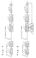
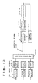
- Fig. 1 is a block diagram of an optical transmitting apparatus as an example useful for understanding the invention.
- Fig. 2 is a block diagram of an optical transmitting apparatus in one embodiment of the present invention.
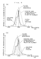
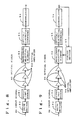
- Fig. 3 is a graph showing a relationship between a generating wavelength of a light source and wavelength transmission characteristics of a wavelength selecting element.
- Fig. 4 is a graph showing a measured signal-to-noise ratio of a demodulated signal with respect to a displacement of the generating wavelength center of an output signal source from the passing wavelength center of a wavelength selecting element.
- Fig. 6 is a block diagram of an optical transmitting apparatus of the present invention.
- Fig. 7 is a block diagram of an optical transmitting apparatus in another example useful for understanding the invention.
- Fig. 5 is another example of a block diagram of an optical transmitting apparatus useful for understanding the invention.
- Fig. 8 is a block diagram of an optical transmitting apparatus in another embodiment of the present invention.
- Fig. 9 is a block diagram of an optical transmitting apparatus in another embodiment of the present invention.
- Fig. 10 is a block diagram of an optical transmitting apparatus in another example useful for understanding the invention.
- Fig. 11 is a block diagram of an optical transmitting apparatus in another example useful for understanding the present invention.
- Fig. 12 is a block diagram of an optical transmitting apparatus in another embodiment of the present invention.
- Fig. 13 is a block diagram of an optical transmitting apparatus in another embodiment of the present invention.
- Fig. 14 is a block diagram of an optical transmitting apparatus in another embodiment of the present invention.
- Fig. 15 is a block diagram of an optical transmitting apparatus in another example useful for understanding the present invention.
- Fig. 16 is a block diagram'of an optical transmitting apparatus in another embodiment of the present invention.
- Fig. 17 is a block diagram of an optical transmitting apparatus in another embodiment of the present invention.
- Fig. 18 is a graph showing a relationship between a generating wavelength of a light source and wavelength transmission characteristics of a wavelength selecting element.
- Fig. 19 is a graph showing a relationship between a generating wavelength of a light source group and wavelength transmission characteristics in each channel of a branching device.
- Fig. 1 shows a block diagram of a first example useful in understanding the present invention.
- an input signal 10 is inputted into a drive section 12, which directly modulates a light source 11 such as a semiconductor laser, and thus converted to an optical signal, and transmitted through an optical fiber 13. Due to a carrier fluctuation, the directly modulated optical signal develops a distortion or spread in an optical spectrum.
- the optical signal transmitted through the optical fiber is filtered by a wavelength selecting element 14, and converted by an optical/electrical converting section 15 to an electric signal. Further, it is demodulated by a demodulator 16 to a required signal.
- the center of the wavelength passing band of the wavelength selecting element 14 is set to a position displaced from a peak in the optical spectrum of the output light source, so that a required parameter in the demodulated signal becomes optimum.
- the central passing band wavelength of the wavelength selecting element 14 is set in such a manner that the error rate or pulse jitter of the demodulated signal becomes minimum, or a certain value or less, or that the signal-to-noise ratio becomes maximum, or a certain value or more.
- an error-detectable modulation code mode such as a block code including a CMI code or an 8B10B, and using such signal, the output light source 11 is directly modulated.
- the modulated optical signal is transmitted through the optical fiber 13 and demodulated by the demodulator 16 to a digital signal.
- an error correction is performed.
- the central passing band wavelength of the wavelength selecting element 14 is set in such a manner that the error correction becomes minimum, or a certain value or less.
- Part of a clock signal regenerated together with the demodulated signal is caused to pass through an electrical filter such as a band-pass filter so as to take out a fundamental frequency component.
- an electrical filter such as a band-pass filter so as to take out a fundamental frequency component.
- a residual FM noise generated in the signal by a jitter component is detected, and the central passing band wavelength of the wavelength selecting element 14 is set in such a manner that the noise level becomes minimum,or a certain value or less.
- the output light source in this example is not limited to a semiconductor laser, and may be a light emitting diode.
- the central passing band wavelength of the wavelength selecting element 14 is set in such a manner that the carrier wave signal-to-noise becomes maximum, or a certain value or more, or that the distortion becomes minimum, or a certain value or less.
- part of the output from the optical/electrical converting section 15 is inputted into the electrical filter to detect the frequency component of a carrier wave signal and the signal level within a certain band. These two signal components are direct-current converted by an integrator and the like to compare them to each other through division process.
- the central passing band wavelength of the wavelength selecting element 14 is set in such a manner that the divided value becomes maximum, or a certain value or more.
- the higher harmonic component of a carrier wave within the highfrequency region developed due to a transmission distortion is detected.
- the higher harmonic component is direct-current converted by an integrator and the like to compare to the carrier wave signal level through division process.
- the central passing band wavelength of the wavelength selecting element 14 is set in such a manner that the divided value becomes maximum, or a certain value or more.
- the central passing band wavelength of the wavelength selecting element 14 is set in such a manner that either the signal-to-noise ratio of the demodulated signal or the signal-to-noise ratio of a certain carrier wave signal becomes maximum, or a certain value or more, or that the distortion becomes minimum, or a certain value or less, or that a predetermined parameter in the multiplexed pilot signal becomes optimum.
- part of the output from the optical/electrical converting section 15 is inputted into the electrical filter to detect either the frequency component of a carrier wave signal of a predetermined channel or a controlling pilot signal multiplexed previously when outputted and the signal level within a certain band.
- These two signal components are direct-current converted by an integrator and the like to compare them to each other through division process.
- the central passing band wavelength of the wavelength selecting element 14 is set in such a manner that the divided value becomes maximum, or a certain value or more.
- the central passing band wavelength of the wavelength selecting element 14 is set in such a manner that the divided value becomes maximum, or a certain value or more.
- the central wavelength of the wavelength selecting element is set to the short wavelength side with respect to the spectrum peak of the light outputting source 11.
- the signal is transmitted through the optical fiber 13 followed by the wavelength selecting element 14, the signal processing procedure is not limited to such a manner. Even where the output light from the output light source 11 is directly inputted into the wavelength selecting element 14, and then transmitted through the optical fiber 13, a similar effect can be obtained.
- Fig. 4 shows an example of results obtained by verifying experimentally the present invention. It shows results obtained by measuring both the displacement of the light source from the central wavelength of the wavelength selecting element and the signal-to-noise ratio where a DFB laser is direct-current biased near at a threshold, directly pulsed and modulated.
- An optical filter having a passing band (full width at half maximum) of 1.3 nanometer was used as the wavelength selecting element.
- the central passing band wavelength of the wavelength selecting element 14 is set to the short wavelength side, thereby allowing a good signal demodulation. This is a phenomenon developed due to a fact that when a pulse is modulated, the chirping effect causes a transient signal component of the pulse to be contained in the short wavelength side with respect to the wavelength peak.
- the central wavelength of the wavelength selecting element 14 is set in such a manner that the wavelength is displaced to the long wavelength side from the peak wavelength of the light outputting source, thereby making the jitter of the demodulated signal small.
- Fig. 2 shows an embodiment of the present embodiment.
- an input signal 20 is inputted into a drive section 22, which directly modulates a light source 21 such as a semiconductor laser.
- the electric signal is converted to an optical signal, and transmitted through an optical fiber 23. Due to a carrier fluctuation, the directly modulated optical signal develops a distortion or spread in an optical spectrum.
- the optical signal is passed through a wavelength selecting element 24 to be optically filtered, and then converted by an optical/electrical converting section 25 to an electric signal and demodulated by a demodulator 26 to a required signal.
- the passing wavelength of the wavelength selecting element 24 is follow-up controlled by a control section 27 in such a manner that a required signal parameter in the demodulated signal becomes optimum.
- the central passing band wavelength of the wavelength selecting element 24 is follow-up controlled in such a manner that the error rate or pulse jitter of the demodulated signal becomes minimum, or a certain value or less, or that the signal-to-noise ratio becomes maximum, or a certain value or more.
- an error-detectable modulation code mode such as a block code including a CMI code or an 8B10B, and using such signal, the light outputting source 21 is directly modulated.
- the modulated optical signal is transmitted through the optical fiber 23 and demodulated by the demodulator 26 to a digital signal.
- an error correction is performed.
- the central passing band wavelength of the wavelength selecting element 24 is follow-up controlled in such a manner that the error correction becomes minimum, or a certain value or less.
- Part of a clock signal regenerated together with the demodulated signal is caused to pass through an electrical filter such as a band-pass filter so as to take out a fundamental frequency component.
- an electrical filter such as a band-pass filter so as to take out a fundamental frequency component.
- a residual FM noise generated by the jitter in the component is detected, and the central passing band wavelength of the wavelength selecting element 24 is follow-up controlled in such a manner that the noise level becomes minimum, or a certain value or less.
- the central passing band wavelength of the wavelength selecting element 24 is follow-up controlled in such a manner that the fluctuating component becomes minimum, or a certain value or less.
- the central passing band wavelength of the wavelength selecting element 24 is follow-up controlled in such a manner that the carrier wave signal-to-noise becomes maximum, or a certain value or more, or that the distortion becomes minimum, or a certain value or less.
- part of the output from the optical/electrical converting section 25 is inputted into the electrical filter to detect the frequency component of a carrier wave signal and the signal level within a certain band, and these two signal components are direct-current converted by an integrator and the like to compare them to each other through division process.
- the central passing band wavelength of the wavelength selecting element 24 is follow-up controlled in such a manner that the divided value becomes maximum, or a certain value or more.
- the higher harmonic component of a carrier wave within the highfrequency region developed due to a transmission distortion is detected, and the higher harmonic component is direct-current converted by an integrator and the like to compare to the carrier wave signal level through division process.
- the central passing band wavelength of the wavelength selecting element 24 is follow-up controlled in such a manner that the divided value becomes maximum, or a certain value or more.
- the central passing band wavelength of the wavelength selecting element 24 is follow-up controlled in such a manner that either the signal-to-noise ratio of the demodulated signal or the signal-to-noise ratio of a certain carrier wave signal becomes maximum, or that the distortion becomes minimum, or that a predetermined parameter in the multiplexed pilot signal becomes optimum.
- part of the output from the optical/electrical converting section 25 is inputted into the electrical filter to detect either the frequency component of a carrier wave signal of a predetermined channel or a controlling pilot signal multiplexed previously when outputted and the signal level within a certain band.
- These two signal components are direct-current converted by an integrator and the like to compare them to each other through division process.
- the central passing band wavelength of the wavelength selecting element 24 is follow-up controlled in such a manner that the divided value becomes maximum, or a certain value or more.
- a distortion signal component developed due to a transmission distortion is detected, and direct-current converted by an integrator and the like to compare to the carrier wave signal level through division process.
- the central passing band wavelength of the wavelength selecting element 24 is follow-up controlled in such a manner that the divided value becomes maximum, or a certain value or more.
- An optical amplifier may be used in the embodiments of the present invention.
- An embodiment using such an amplifier is shown in Fig. 6 and such an amplifier is used in the example of Fig. 5.
- the embodiment is characterized in that amplifiers 58, 68 are inserted, and the arrangement allows a long-distance transmission.
- the insertion of an optical amplifier as mentioned above allows the optical signal to be distributed and transmitted through a plurality of signal receiving sections as shown in Fig. 7.
- the position into which wavelength selecting elements 54, 64 are inserted is not always limited to such an arrangement. Even where they are located at the input of the optical amplifiers 58, 68, similar results are obtained.
- a wavelength selecting element 84 is not limited in location to only a position before the input of a signal receiver, but may be inserted into the input/output of the optical amplifiers 88 or between them.
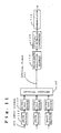
- Fig. 11 shows another example useful in understanding the present invention.
- an input signal group 110 is inputted into respective drive sections 112, which directly modulate directly-modulatable output light sources 111 such as a semiconductor laser, and thus converted to an optical signal.
- the output light sources 111 generate signal lights having wavelengths ⁇ 1, ⁇ 2 and ⁇ 3 corresponding to respective channels. These signal lights are coupled to an optical fiber 113 by an optical coupler 117 or an optical combining device, and thus multiplexed in wavelength and transmitted. Due to a carrier fluctuation, the directly modulated optical signal develops a distortion or spread in an optical spectrum.
- a signal light of a required channel is selected in wavelength through a wavelength selecting element 114 (an optical tuner).
- the signal light is then converted by an optical/electrical converting section 115 to an electrical signal, and demodulated by a modulator 116 to a required signal.
- the central passing band wavelength of the wavelength selecting element 114 is set to a position displayed from the peak in the optical spectrum of an output light source selected by the wavelength selecting element 114 in such a manner that a required parameter in the demodulated signal becomes optimum as shown in Fig. 3.
- Fig. 12 shows another embodiment of the present embodiment.
- an input signal group 120 is inputted into respective drive sections 122, which directly modulate directly-modulatable output light sources 121 such as a semiconductor laser, and thus converted to an optical signal.
- the output light sources 121 generate signal lights having wavelengths ⁇ 1, ⁇ 2 and ⁇ 3 corresponding to respective channels. These signal lights are coupled to an optical fiber 123 by an optical coupler 128 or an optical combining device, and thus multiplexed in wavelength and transmitted. Due to a carrier fluctuation, the directly-modulated optical signal develops a distortion or spread in an optical spectrum.
- a signal light of a required channel is selected in wavelength through a wavelength selecting element 124 (an optical tuner).
- the signal light is then converted by an optical/electrical converting section 125 to an electrical signal, and demodulated by a modulator 126 to a required signal.
- the central passing band wavelength of the wavelength selecting element 124 is set to and follow-up controlled a position displayed from the peak in the optical spectrum of an output light source selected by the wavelength selecting element 124 in such a manner that a required parameter in the demodulated signal becomes optimum as shown in Fig. 3 (b).
- the signal may be transmitted to a plurality of light receiving sections as shown in Fig. 13. Further, as shown in Fig. 14, the use of an optical amplifier 148 allows the signal to be transmitted through a longer distance to a number of light receiving sections.
- Fig. 15 shows another example useful in understanding the present invention.
- an input signal group 150 is inputted into respective drive sections 152, which directly modulate directly-modulatable output light sources 151 such as a semiconductor laser, and thus converted to an optical signal.
- the output light sources 151 generate signal lights having wavelengths ⁇ 1, ⁇ 2 and ⁇ 3 corresponding to respective channels.
- These signal lights are coupled to an optical fiber 153 by an optical coupler 158 or a light combiner, and thus multiplexed in wavelength and transmitted. Due to a carrier fluctuation, the directly modulated optical signal develops a distortion or spread in an optical spectrum.
- a signal light of each channel is selected in wavelength through an optical branching device 159.
- the signal light is then converted by an optical/electrical converting section 155 to an electrical signal, and demodulated by a demodulator 156 to a required signal.
- the central passing band wavelength of each channel of the optical branching device 159 is set to a position displayed from the peak in the optical spectrum of an output light source selected in such a manner that a required parameter in the demodulated signal becomes optimum as shown in Fig. 19.
- the selected wavelength center of each channel of the branching device is set to the short wavelength side with respect to the wavelength center of each output light, the selected wavelength center may be set to the long wavelength side depending upon modulation system, drive conditions of light source and chirping characteristics.
- Fig. 16 shows another embodiment of the present invention.
- an input signal group 160 is inputted into respective drive sections 162, which directly modulate directly-modulatable output light sources 161 such as a semiconductor laser, and thus converted to an optical signal.
- the output light sources 161 generate signal lights having wavelengths ⁇ 1, ⁇ 2 and ⁇ 3 corresponding to respective channels. These signal lights are coupled to an optical fiber 163 by an optical coupler 168 or an optical combining device, and thus multiplexed in wavelength and transmitted. Due to a carrier fluctuation, the directly-modulated optical signal develops a distortion or spread in an optical spectrum.
- a signal light of each channel is selected in wavelength through an optical branching device 169, and then each channel is converted by an optical/electrical converting section 165 to an electrical signal, and demodulated by a modulator 166 to a required signal.
- the central passing band wavelength of each channel of the optical branching device 169 is set to and follow-up controlled a position displayed from the peak in the optical spectrum of a light outputting source selected in such a manner that a required parameter becomes optimum using the modulated signal of a certain channel as shown above.
- the signal may be amplified by an optical amplifier 178 and distributed by an optical distributor 181, thereby being transmitted to a plurality of receiving sections as shown in Fig. 17.
- the output light source of the present invention employs an external resonance type semiconductor laser or a directly-modulatable longitudinal single mode generating type semiconductor laser such as a DFB laser and a DBR laser.
- an external resonance type semiconductor laser or a directly-modulatable longitudinal single mode generating type semiconductor laser such as a DFB laser and a DBR laser.
- used in the optical amplifier of the present invention is an optical fiber in which a rare earth element is doped.
- erbium, praseodymium or neodymium is used as the rare earth element.
- used in the optical amplifier of the present invention is a semiconductor type amplifier.
- wavelength selecting element of the present invention is a grating, a dielectric filter, a Fabry Perot etalon, an electric optics, an acoustic optics, an optical waveguide element, or a double reflective optics.
- conditions for the drive current and the like of the output light source are set in such a manner that a required parameter of the demodulated signal received becomes optimum.
Landscapes
- Physics & Mathematics (AREA)
- Electromagnetism (AREA)
- Engineering & Computer Science (AREA)
- Computer Networks & Wireless Communication (AREA)
- Signal Processing (AREA)
- Spectroscopy & Molecular Physics (AREA)
- Optical Communication System (AREA)
Claims (12)
- Optische Übertragungsvorrichtung, die umfasst:gekennzeichnet durch:eine direkt modulierbare Ausgangslichtquelle (11), die ein zu übertragendes Lichtsignal erzeugt,eine Lichtleitfaser (13), die das von der Ausgangslichtquelle (11) erzeugte Lichtsignal überträgt,ein Wellenlängen-Auswählelement (14), das optisches Filtem des übertragenen Lichtsignals ausführt,einen optoelektronischen Wandler (15), der optoelektronische Umwandlung des übertragenen Lichtsignals ausführt,den Demodulator (16), der das von dem optoelektronischen Wandler (15) umgewandelte elektrische Signal in ein benötigtes Signal demoduliert, undeinen Steuerabschnitt (17), der zwischen den Ausgang des Demodulators (6) und das Wellenlängen-Auswählelement (14) geschaltet ist und die Mittenwellenlänge eines Durchlassbereiches des Wellenlängen-Auswählelementes (14), die gegenüber der Mittenwellenlänge einer von der Ausgangslichtquelle (11) erzeugten Wellenlänge verschoben ist, einstellt und Folgesteuerung unterzieht, so dass ein erforderlicher Signalparameter in dem demodulierten Signal ein Optimum erreicht.
- Optische Übertragungsvorrichtung nach Anspruch 1, wobei:die Ausgangslichtquelle (11) durch ein Ausgangssignal direkt moduliert wird und die Mittenwellenlänge eines Durchlassbereiches des Wellenlängen-Auswählelementes (14) entweder auf eine Seite kurzer Wellenlänge oder eine Seite langer Wellenlänge in Bezug auf die Mittenwellenlänge der von der Ausgangslichtquelle erzeugten Wellenlänge eingestellt wird.
- Optische Übertragungsvorrichtung nach Anspruch 1,
dadurch gekennzeichnet, dass:die Mittenwellenlänge eines Durchlassbereiches des Wellenlängen-Auswählelementes durch den Steuerabschnitt (27) so gesteuert wird, dass ein Signal-Rausch-Verhältnis oder ein Trägersignal-Rausch-Verhältnis in dem von dem Demodulator demodulierten Signal ein Maximum erreicht oder über einem bestimmten Wert liegt. - Optische Übertragungsvorrichtung nach Anspruch 1 oder 3,
dadurch gekennzeichnet, dass:die Mittenwellenlänge eines Durchlassbereiches des Wellenlängen-Auswählelementes von dem Steuerabschnitt (27) so gesteuert wird, dass eine Fehlerrate in dem von dem Demodulator demodulierten Signal ein Minimum erreicht oder unter einem bestimmten Wert liegt, oder dass eine Verzerrung in dem demodulierten Signal ein Minimum erreicht oder unter einem bestimmten Wert liegt, oder dass ein Jitter in dem demodulierten Signal ein Minimum erreicht oder unter einem bestimmten Wert liegt. - Optische Übertragungsvorrichtung nach einem der Ansprüche 1 bis 4, wobei eine Lichtquelle, die ein Licht mit einer einzelnen Wellenlänge erzeugt, als die Ausgangslichtquelle (11) eingesetzt wird.
- Optische Übertragungsvorrichtung nach einem der Ansprüche 1 bis 5,
dadurch gekennzeichnet, dass:die Ausgangslichtquelle eine Vielzahl von Ausgangslichtquellen enthält, die direkt moduliert werden können und jeweils Licht mit einzelnen Wellenlängen erzeugen, die sich voneinander unterscheiden, unddie Vorrichtung des Weiteren einen optischen Koppler (117) umfasst. - Optische Übertragungsvorrichtung nach Anspruch 6,
dadurch gekennzeichnet, dass:das Wellenlängen-Auswählelement (14) eine optische Verzweigungsvorrichtung (169) ist, die mit einer Vielzahl von Signalempfangsabschnitten verbunden ist, die jeweils einen optoelektronischen Wandler (165) und einen Demodulator (166) umfassen. - Optische Übertragungsvorrichtung nach Anspruch 7, wobei:die Ausgangslichtquelle direkt durch ein Ausgangssignal moduliert wird, unddie Mittenwellenlänge eines Durchlassbereiches, die jedem Kanal der optischen Verzweigungsvorrichtung entspricht, entweder auf eine Seite kurzer Wellenlänge oder eine Seite langer Wellenlänge in Bezug auf die Mittenwellenlänge jeder von der Ausgangslichtquelle erzeugten Wellenlänge eingestellt wird.
- Optische Übertragungsvorrichtung nach Anspruch 7, wobei:sowohl ein Ansteuerstrom der Ausgangslichtquelle als auch die Mittenwellenlänge eines Durchlassbereiches entsprechend jedem Kanal der optischen Verzweigungsvorrichtung durch den Steuerabschnitt (27) so eingestellt werden, dass ein Signal-Rausch-Verhältnis des demodulierten Signals ein Maximum erreicht oder über einem bestimmten Wert liegt, oder dass ein Trägersignal-Rausch-Verhältnis des demodulierten Signals ein Maximum erreicht oder über einem bestimmten Wert liegt, oder dass eine Fehlerrate des demodulierten Signals ein Minimum erreicht oder unter einem bestimmten Wert liegt, oder dass eine Verzerrung des demodulierten Signals ein Minimum erreicht oder unter einem bestimmten Wert liegt, oder dass ein Jitter des demodulierten Signals ein Minimum erreicht oder unter einem bestimmten Wert liegt.
- Optische Übertragungsvorrichtung nach Anspruch 7,
wobei die Mittenwellenlänge eines Durchlassbereiches entsprechend jedem Kanal der optischen Verzweigungsvorrichtung durch den Steuerabschnitt (27) so gesteuert wird, dass ein Signal-Rausch-Verhältnis in einem von dem Demodulator demodulierten Signal ein Maximum erreicht oder über einem bestimmten Wert liegt, oder dass ein Trägersignal-Rausch-Verhältnis in dem demodulierten Signal ein Maximum erreicht oder über einem bestimmten Wert liegt, oder dass eine Fehlerrate in dem demodulierten Signal ein Minimum erreicht oder unter einem bestimmten Wert liegt, oder dass eine Verzerrung in dem demodulierten Signal ein Minimum erreicht oder unter einem bestimmten Wert liegt, oder dass ein Jitter des demodulierten Signals ein Minimum erreicht oder unter einem bestimmten Wert liegt. - Optische Übertragungsvorrichtung nach einem der Ansprüche 1 bis 10,
dadurch gekennzeichnet, dass:die Vorrichtung des Weiteren wenigstens einen optischen Verstärker (58, 68) umfasst, der das übertragene Lichtsignal verstärkt. - Optische Übertragungsvorrichtung nach einem der Ansprüche 1 bis 11,
dadurch gekennzeichnet, dass:eine Vielzahl von Signalempfangsabschnitten, die jeweils ein Wellenlängen-Auswählelement (144), einen optoelektronischen Wandler (145) und einen Demodulator (146) umfassen, mit der Lichtleitfaser (143) verbunden ist, und dass wenigstens eines der Wellenlängen-Auswähtelemente (144) von dem Steuerabschnitt (147) gesteuert wird.
Applications Claiming Priority (3)
| Application Number | Priority Date | Filing Date | Title |
|---|---|---|---|
| JP10385193A JP3368935B2 (ja) | 1993-04-30 | 1993-04-30 | 光伝送装置 |
| JP103851/93 | 1993-04-30 | ||
| JP10385193 | 1993-04-30 |
Publications (2)
| Publication Number | Publication Date |
|---|---|
| EP0622913A1 EP0622913A1 (de) | 1994-11-02 |
| EP0622913B1 true EP0622913B1 (de) | 2002-07-31 |
Family
ID=14364949
Family Applications (1)
| Application Number | Title | Priority Date | Filing Date |
|---|---|---|---|
| EP94106769A Expired - Lifetime EP0622913B1 (de) | 1993-04-30 | 1994-04-29 | Vorrichtung für optische Übertragung mit direkter Modulation des Senders und optischer Filterung beim Empfänger |
Country Status (3)
| Country | Link |
|---|---|
| EP (1) | EP0622913B1 (de) |
| JP (1) | JP3368935B2 (de) |
| DE (1) | DE69431085T2 (de) |
Families Citing this family (6)
| Publication number | Priority date | Publication date | Assignee | Title |
|---|---|---|---|---|
| JP3072047B2 (ja) * | 1995-03-22 | 2000-07-31 | 株式会社東芝 | 波長多重光伝送装置および光中継器 |
| JPH0951325A (ja) * | 1995-08-09 | 1997-02-18 | Nec Corp | 波長多重光伝送システム |
| DE19722560A1 (de) * | 1997-05-28 | 1998-12-03 | Alsthom Cge Alcatel | Empfänger für ein optisches Nachrichtenübertragungssystem, Filtervorrichtung und Verfahren zu dessen Betrieb |
| EP1041761A3 (de) * | 1999-03-31 | 2005-07-20 | Matsushita Electric Industrial Co., Ltd. | Wellenlängenabstimmbare Filtereinrichtung |
| JP2007158251A (ja) * | 2005-12-08 | 2007-06-21 | Nippon Telegr & Teleph Corp <Ntt> | 波長安定化装置及び波長安定化方法 |
| KR101392498B1 (ko) * | 2008-12-12 | 2014-05-12 | 한국전자통신연구원 | 반사 민감도가 개선된 파장분할 다중방식 기반 수동형 광가입자망에서의 광 송신장치 및 광 송신방법 |
Family Cites Families (3)
| Publication number | Priority date | Publication date | Assignee | Title |
|---|---|---|---|---|
| US5027435A (en) * | 1987-07-15 | 1991-06-25 | At&T Bell Laboratories | Optical communication systems using Fabry-Perot cavities |
| EP0530025B1 (de) * | 1991-08-29 | 1997-10-29 | Nec Corporation | Lichtempfangsmodul |
| GB2260046B (en) * | 1991-09-26 | 1995-02-15 | Northern Telecom Ltd | Optical communications systems |
-
1993
- 1993-04-30 JP JP10385193A patent/JP3368935B2/ja not_active Expired - Fee Related
-
1994
- 1994-04-29 DE DE69431085T patent/DE69431085T2/de not_active Expired - Fee Related
- 1994-04-29 EP EP94106769A patent/EP0622913B1/de not_active Expired - Lifetime
Also Published As
| Publication number | Publication date |
|---|---|
| JP3368935B2 (ja) | 2003-01-20 |
| DE69431085T2 (de) | 2002-11-21 |
| EP0622913A1 (de) | 1994-11-02 |
| JPH06315010A (ja) | 1994-11-08 |
| DE69431085D1 (de) | 2002-09-05 |
Similar Documents
| Publication | Publication Date | Title |
|---|---|---|
| US6389046B1 (en) | Method to sense laser array power and wavelength and reduce drift for wavelength selection and stabilization | |
| EP0703678B1 (de) | Leistungsüberwachung und Fehlerortung in optischen Übertragungssystemen | |
| EP1427119B1 (de) | Optischer Verstärker und optisches Übertragungssystem unter Verwendung dieses Verstärkers | |
| US6795607B1 (en) | Use of tunable laser for optical performance monitoring in WDM system | |
| EP0532021B1 (de) | Kohärentes optisches Übertragungssystem mit mehrfach ausgenutzten Hilfsträgern | |
| US6198757B1 (en) | Control system for wavelength stabilization of a laser source | |
| US7203429B2 (en) | Optical transmission system using optical signal processing in terminals for improved system performance | |
| EP1393483B1 (de) | Empfänger und verfahren zum empfang eines optischen multikanalsignals | |
| IL124639A (en) | Optical communication method and system using wavelength division multiplexing | |
| US20020063928A1 (en) | Filtering of data-encoded optical signals | |
| EP0622913B1 (de) | Vorrichtung für optische Übertragung mit direkter Modulation des Senders und optischer Filterung beim Empfänger | |
| US7409156B2 (en) | System and method for a supervisory signal modulation scheme using variable optical attenuators | |
| US20060188267A1 (en) | System and method for suppression of stimulated Brillouin scattering in optical transmission communications | |
| JP3983510B2 (ja) | 光増幅装置 | |
| US6542272B1 (en) | Control signal transmission method and apparatus for optical transmission system | |
| US6907157B2 (en) | Method and system for optical fiber transmission using raman amplification | |
| US20060051095A1 (en) | Modulation with low cross-talk in optical transmission | |
| JPH10290213A (ja) | 光通信用デバイスおよび光通信装置および光通信システム並びに光スペクトルアナライザ | |
| EP0602659A1 (de) | Verfahren zum Unterdrückes der Frequenzmodulation von amplitudenmodulierten optischen Signalen | |
| JP3917628B2 (ja) | 光増幅器及び該光増幅器を備えた光通信システム | |
| JP2005045721A (ja) | 波長分割多重信号光のパワー傾斜をモニタするシステムおよび方法 | |
| JP2000183813A (ja) | 帯域幅が可変な受信フィルタを備えた光ファイバ伝送システム | |
| KR100460492B1 (ko) | 광 파장분할다중화 전송장비에서의 광파장 잠금장치 및 그방법 | |
| JP2000341218A (ja) | 光送受信システム、光受信装置、および光送受信方法 | |
| JPH0897776A (ja) | 光中継器 |
Legal Events
| Date | Code | Title | Description |
|---|---|---|---|
| PUAI | Public reference made under article 153(3) epc to a published international application that has entered the european phase |
Free format text: ORIGINAL CODE: 0009012 |
|
| AK | Designated contracting states |
Kind code of ref document: A1 Designated state(s): DE FR GB NL |
|
| 17P | Request for examination filed |
Effective date: 19950209 |
|
| 17Q | First examination report despatched |
Effective date: 19971017 |
|
| GRAG | Despatch of communication of intention to grant |
Free format text: ORIGINAL CODE: EPIDOS AGRA |
|
| GRAG | Despatch of communication of intention to grant |
Free format text: ORIGINAL CODE: EPIDOS AGRA |
|
| GRAH | Despatch of communication of intention to grant a patent |
Free format text: ORIGINAL CODE: EPIDOS IGRA |
|
| RIN1 | Information on inventor provided before grant (corrected) |
Inventor name: MORIKURA, SUSUMU Inventor name: IIDA, MASANORI Inventor name: ASAKURA, HIROYUKI |
|
| GRAH | Despatch of communication of intention to grant a patent |
Free format text: ORIGINAL CODE: EPIDOS IGRA |
|
| GRAA | (expected) grant |
Free format text: ORIGINAL CODE: 0009210 |
|
| AK | Designated contracting states |
Kind code of ref document: B1 Designated state(s): DE FR GB NL |
|
| REG | Reference to a national code |
Ref country code: GB Ref legal event code: FG4D |
|
| REF | Corresponds to: |
Ref document number: 69431085 Country of ref document: DE Date of ref document: 20020905 |
|
| ET | Fr: translation filed | ||
| PLBE | No opposition filed within time limit |
Free format text: ORIGINAL CODE: 0009261 |
|
| STAA | Information on the status of an ep patent application or granted ep patent |
Free format text: STATUS: NO OPPOSITION FILED WITHIN TIME LIMIT |
|
| 26N | No opposition filed |
Effective date: 20030506 |
|
| PGFP | Annual fee paid to national office [announced via postgrant information from national office to epo] |
Ref country code: NL Payment date: 20090427 Year of fee payment: 16 Ref country code: FR Payment date: 20090417 Year of fee payment: 16 Ref country code: DE Payment date: 20090428 Year of fee payment: 16 |
|
| PGFP | Annual fee paid to national office [announced via postgrant information from national office to epo] |
Ref country code: GB Payment date: 20090429 Year of fee payment: 16 |
|
| REG | Reference to a national code |
Ref country code: NL Ref legal event code: V1 Effective date: 20101101 |
|
| GBPC | Gb: european patent ceased through non-payment of renewal fee |
Effective date: 20100429 |
|
| REG | Reference to a national code |
Ref country code: FR Ref legal event code: ST Effective date: 20101230 |
|
| PG25 | Lapsed in a contracting state [announced via postgrant information from national office to epo] |
Ref country code: NL Free format text: LAPSE BECAUSE OF NON-PAYMENT OF DUE FEES Effective date: 20101101 |
|
| PG25 | Lapsed in a contracting state [announced via postgrant information from national office to epo] |
Ref country code: DE Free format text: LAPSE BECAUSE OF NON-PAYMENT OF DUE FEES Effective date: 20101103 |
|
| PG25 | Lapsed in a contracting state [announced via postgrant information from national office to epo] |
Ref country code: GB Free format text: LAPSE BECAUSE OF NON-PAYMENT OF DUE FEES Effective date: 20100429 |
|
| PG25 | Lapsed in a contracting state [announced via postgrant information from national office to epo] |
Ref country code: FR Free format text: LAPSE BECAUSE OF NON-PAYMENT OF DUE FEES Effective date: 20100430 |