EP0624899A2 - Oxidation von Silizium-Nitrid in der Herstellung von Halbleitenden Anordnungen - Google Patents
Oxidation von Silizium-Nitrid in der Herstellung von Halbleitenden Anordnungen Download PDFInfo
- Publication number
- EP0624899A2 EP0624899A2 EP94104574A EP94104574A EP0624899A2 EP 0624899 A2 EP0624899 A2 EP 0624899A2 EP 94104574 A EP94104574 A EP 94104574A EP 94104574 A EP94104574 A EP 94104574A EP 0624899 A2 EP0624899 A2 EP 0624899A2
- Authority
- EP
- European Patent Office
- Prior art keywords
- silicon nitride
- layer
- oxide
- trench
- oxidation
- Prior art date
- Legal status (The legal status is an assumption and is not a legal conclusion. Google has not performed a legal analysis and makes no representation as to the accuracy of the status listed.)
- Granted
Links
Images

Classifications
-
- H—ELECTRICITY
- H10—SEMICONDUCTOR DEVICES; ELECTRIC SOLID-STATE DEVICES NOT OTHERWISE PROVIDED FOR
- H10P—GENERIC PROCESSES OR APPARATUS FOR THE MANUFACTURE OR TREATMENT OF DEVICES COVERED BY CLASS H10
- H10P14/00—Formation of materials, e.g. in the shape of layers or pillars
- H10P14/60—Formation of materials, e.g. in the shape of layers or pillars of insulating materials
- H10P14/65—Formation of materials, e.g. in the shape of layers or pillars of insulating materials characterised by treatments performed before or after the formation of the materials
- H10P14/6516—Formation of materials, e.g. in the shape of layers or pillars of insulating materials characterised by treatments performed before or after the formation of the materials of treatments performed after formation of the materials
- H10P14/6518—Formation of materials, e.g. in the shape of layers or pillars of insulating materials characterised by treatments performed before or after the formation of the materials of treatments performed after formation of the materials by introduction of substances into an already-existing insulating layer
- H10P14/6519—Formation of materials, e.g. in the shape of layers or pillars of insulating materials characterised by treatments performed before or after the formation of the materials of treatments performed after formation of the materials by introduction of substances into an already-existing insulating layer the substance being oxygen
- H10P14/6522—Formation of materials, e.g. in the shape of layers or pillars of insulating materials characterised by treatments performed before or after the formation of the materials of treatments performed after formation of the materials by introduction of substances into an already-existing insulating layer the substance being oxygen introduced into a nitride material, e.g. changing SiN to SiON
-
- H—ELECTRICITY
- H10—SEMICONDUCTOR DEVICES; ELECTRIC SOLID-STATE DEVICES NOT OTHERWISE PROVIDED FOR
- H10P—GENERIC PROCESSES OR APPARATUS FOR THE MANUFACTURE OR TREATMENT OF DEVICES COVERED BY CLASS H10
- H10P14/00—Formation of materials, e.g. in the shape of layers or pillars
- H10P14/60—Formation of materials, e.g. in the shape of layers or pillars of insulating materials
- H10P14/65—Formation of materials, e.g. in the shape of layers or pillars of insulating materials characterised by treatments performed before or after the formation of the materials
- H10P14/6516—Formation of materials, e.g. in the shape of layers or pillars of insulating materials characterised by treatments performed before or after the formation of the materials of treatments performed after formation of the materials
- H10P14/6529—Formation of materials, e.g. in the shape of layers or pillars of insulating materials characterised by treatments performed before or after the formation of the materials of treatments performed after formation of the materials by exposure to a gas or vapour
-
- H—ELECTRICITY
- H10—SEMICONDUCTOR DEVICES; ELECTRIC SOLID-STATE DEVICES NOT OTHERWISE PROVIDED FOR
- H10P—GENERIC PROCESSES OR APPARATUS FOR THE MANUFACTURE OR TREATMENT OF DEVICES COVERED BY CLASS H10
- H10P14/00—Formation of materials, e.g. in the shape of layers or pillars
- H10P14/60—Formation of materials, e.g. in the shape of layers or pillars of insulating materials
- H10P14/65—Formation of materials, e.g. in the shape of layers or pillars of insulating materials characterised by treatments performed before or after the formation of the materials
- H10P14/6516—Formation of materials, e.g. in the shape of layers or pillars of insulating materials characterised by treatments performed before or after the formation of the materials of treatments performed after formation of the materials
- H10P14/6548—Formation of materials, e.g. in the shape of layers or pillars of insulating materials characterised by treatments performed before or after the formation of the materials of treatments performed after formation of the materials by forming intermediate materials, e.g. capping layers or diffusion barriers
-
- H—ELECTRICITY
- H10—SEMICONDUCTOR DEVICES; ELECTRIC SOLID-STATE DEVICES NOT OTHERWISE PROVIDED FOR
- H10P—GENERIC PROCESSES OR APPARATUS FOR THE MANUFACTURE OR TREATMENT OF DEVICES COVERED BY CLASS H10
- H10P14/00—Formation of materials, e.g. in the shape of layers or pillars
- H10P14/60—Formation of materials, e.g. in the shape of layers or pillars of insulating materials
- H10P14/69—Inorganic materials
- H10P14/692—Inorganic materials composed of oxides, glassy oxides or oxide-based glasses
- H10P14/6921—Inorganic materials composed of oxides, glassy oxides or oxide-based glasses containing silicon
- H10P14/69215—Inorganic materials composed of oxides, glassy oxides or oxide-based glasses containing silicon the material being a silicon oxide, e.g. SiO2
-
- H—ELECTRICITY
- H10—SEMICONDUCTOR DEVICES; ELECTRIC SOLID-STATE DEVICES NOT OTHERWISE PROVIDED FOR
- H10P—GENERIC PROCESSES OR APPARATUS FOR THE MANUFACTURE OR TREATMENT OF DEVICES COVERED BY CLASS H10
- H10P14/00—Formation of materials, e.g. in the shape of layers or pillars
- H10P14/60—Formation of materials, e.g. in the shape of layers or pillars of insulating materials
- H10P14/69—Inorganic materials
- H10P14/694—Inorganic materials composed of nitrides
- H10P14/6943—Inorganic materials composed of nitrides containing silicon
- H10P14/69433—Inorganic materials composed of nitrides containing silicon the material being a silicon nitride not containing oxygen, e.g. SixNy or SixByNz
-
- H—ELECTRICITY
- H10—SEMICONDUCTOR DEVICES; ELECTRIC SOLID-STATE DEVICES NOT OTHERWISE PROVIDED FOR
- H10P—GENERIC PROCESSES OR APPARATUS FOR THE MANUFACTURE OR TREATMENT OF DEVICES COVERED BY CLASS H10
- H10P14/00—Formation of materials, e.g. in the shape of layers or pillars
- H10P14/60—Formation of materials, e.g. in the shape of layers or pillars of insulating materials
- H10P14/63—Formation of materials, e.g. in the shape of layers or pillars of insulating materials characterised by the formation processes
- H10P14/6302—Non-deposition formation processes
- H10P14/6304—Formation by oxidation, e.g. oxidation of the substrate
- H10P14/6306—Formation by oxidation, e.g. oxidation of the substrate of the semiconductor materials
- H10P14/6308—Formation by oxidation, e.g. oxidation of the substrate of the semiconductor materials of Group IV semiconductors
- H10P14/6309—Formation by oxidation, e.g. oxidation of the substrate of the semiconductor materials of Group IV semiconductors of silicon in uncombined form, i.e. pure silicon
Definitions
- the present invention relates generally to semiconductor devices and, in particular, to a method for oxidizing silicon nitride in semiconductor devices using an oxidizing ambient with a dilute amount of a fluorine-containing compound.
- Silicon nitride is commonly used in the manufacture of semiconductor devices.
- One such use for silicon nitride is as an insulation stack commonly known as an ONO layer (i.e. a silicon oxide-silicon nitride-silicon oxide layer) which may be used, for example, as a gate insulator or as an insulator for a deep-trench memory storage device.
- ONO layer i.e. a silicon oxide-silicon nitride-silicon oxide layer
- One disadvantage of the use of silicon nitride is that negative charge trapping can occur at a nitride-oxide interface in an ONO layer, either during processing of the device or during operation of the device after manufacture (e.g. due to hot electrons). In some cases, this charge trapping can sufficiently affect threshold voltages within the device that parasitic leakage paths are formed.
- silicon nitride layer within a device is often conveniently exposed to these oxidizing ambients, the prior teaching has been that silicon nitride cannot be removed by oxidation because silicon nitride does not oxidize. However, if the silicon nitride could be converted to silicon oxide by oxidation, then there would no longer be the problem of silicon nitride trapping injected electrons. In many cases, oxidizing silicon nitride to form silicon oxide could more readily be integrated into the fabrication sequence for a structure than the etching away of the silicon nitride followed by the growing of a silicon oxide layer. Also, eliminating the nitride from regions sensitive to trapped charge would avoid the need for a high temperature processing step near the end of the fabrication sequence.
- the oxidation of silicon nitride could provide more flexibility in adjusting the physical dimensions of a device.
- a silicon nitride layer is used as a structural element in a device because of an advantageous material property of the nitride.
- silicon nitride spacers are sometimes used for spacing the ion implants into the source/drain regions on the device. If the silicon nitride layer could be oxidized, then the dimensions of the initial silicon nitride layer, for example an implant spacer, could be adjusted to advantage for use in later processing steps.
- this oxidation would reduce the quantity of charge which is trapped and thus avoid parasitic leakage paths. In other cases, this oxidation would provide more flexibility in fine-tuning the structural dimensions of a device having a silicon nitride layer.
- a method for oxidizing a silicon nitride layer in a semiconductor device using a fluorine-containing compound in this method a silicon nitride layer is exposed to a mixture of an oxygen reactant and a dilute amount of a fluorine-containing compound at a temperature sufficiently high to substantially cause the oxidation of the silicon nitride.
- the oxygen reactant is diatomic oxygen in the preferred embodiment.
- the oxygen reactant could be atomic oxygen, ozone, ionized oxygen radicals such as would be obtained in a plasma, or a mixture thereof either with or without diatomic oxygen.
- a temperature greater than about 600°C is sufficient to cause such oxidation, although some oxidation may occur at lower temperatures.
- the upper temperature range, the reaction time, and the pressure of the reaction mixture are not critical.
- the concentration of the fluorine-containing compound is also not critical, but is generally between about 100 to 1500 ppm by volume relative to the total mixture volume. In other cases, though, a lower or substantially higher concentration may be used.
- a diluent such as argon may be used as a substantial component of the oxidizing mixture.
- NF3 is a fluorine-containing compound, and a temperature greater than about 700°C is used, preferably in the range of about 800°C to 1000°C.
- concentration of NF3 in the mixture by volume is generally less than about 1500 ppm, although this is not a critical upper limit. More preferably, this concentration is between about 100 to 1000 ppm.
- An important advantage of the present invention is that any trapped charges present in a silicon nitride layer are substantially released following its oxidation.
- the silicon nitride is converted to silicon oxide. It is known that silicon oxide traps less charge than silicon nitride. Thus, less charge will be trapped during subsequent fabrication processing steps and during device operation. Removal of these charges often eliminates undesirable parasitic leakage paths within the device.
- Another advantage is that the temperature required to oxidize the silicon nitride layer is low relative to other processing steps such as growing an oxide without the addition of NF3. Also, oxidation of a layer having silicon nitride affects the physical size of the layer in a predictable manner such that oxidation can be used to adjust the size of such a layer in certain cases.
- an ancillary benefit of the present invention is that silicon corners within the device are rounded during the oxidation of the silicon due to the presence of the fluorine in the oxidizing mixture.
- the amount of oxide grown on silicon compared to the amount grown on silicon nitride can be controlled by controlling the amount of NF3 and the oxidizing temperature.
- a silicon nitride layer in a semiconductor device is oxidized by exposing it to an oxidizing mixture containing an oxygen reactant and a fluorine-containing compound at a temperature sufficiently high to substantially cause the oxidation of the silicon nitride.
- a temperature sufficiently high to substantially cause the oxidation of the silicon nitride.
- a temperature greater than about 600°C is sufficient to cause such oxidation, although some oxidation may occur at lower temperatures. It is believed that the reaction temperature is sufficiently high if a fluorine atom in the fluorine-containing compound becomes sufficiently reactive to weaken a silicon nitride bond in the silicon nitride layer.
- fluorine-containing compound such as NF3, SF6, SiF4, CF4, and C2H3Cl2F.
- the only other significant limitation on chemicals that can be so used is that it can be introduced in gas form into the heated region of the furnace.
- the oxygen reactant is diatomic oxygen in the preferred embodiment.
- the oxygen reactant could be atomic oxygen, ozone, ionized oxygen radicals such as would be obtained in a plasma, or a mixture thereof either with or without diatomic oxygen.
- a plasma for producing oxygen radicals may be generated using a plasma chamber having a heated chuck, such as an AME 5000.
- the concentration of the fluorine-containing compound is not critical and is generally a dilute concentration that can vary over a wide range. More specifically, this concentration may generally range between about 100 to 1500 ppm by volume relative to the total mixture volume. In other cases, though, a lower or substantially higher concentration may be used.
- a diluent may be used as a part of the oxidizing mixture, such as argon or nitrogen.
- the proportion of the diluent in the mixture is not at all critical and may be varied to a great extent. As one example, this proportion may range between about 10 to 95 percent by volume relative to the total reaction mixture. It is believed that the diluent may be beneficial in achieving mixing and carrying of the reacting gasses uniformly to all parts of the wafer.
- a semiconductor wafer containing a silicon nitride layer to be oxidized according to the present invention can be heated in any of a number of ways--the type of heating used is not critical.
- the wafer is heated by rapid thermal annealing (RTA).
- RTA rapid thermal annealing
- the wafer may be heated in a furnace, on a wafer chuck in a plasma with the flourine-containing compound, or by local heating using laser annealing.
- the time that the wafer is exposed to the oxidizing mixture is also not critical and depends upon a number of factors including the type of heating system used, the concentration of the fluorine-containing compound, and the temperature to which the wafer is heated during oxidation. Generally, when heating by RTA, oxidation times are about 1 to 10 minutes, and when heating using a furnace, oxidation times are about 20 to 40 minutes. However, times outside these ranges can be used depending upon the particular process conditions and targets. Also, the pressure of the oxidizing mixture is not critical. In the preferred embodiment, the mixture is at about atmospheric pressure, but it is expected that a wide range of pressures may be used.
- topography of a silicon nitride layer to be oxidized according to the present invention on a semiconductor wafer can vary greatly depending upon prior processing and the device type being formed. However, it is expected that the reaction of the present invention can be used with almost any topography, whether vertical or horizontal or otherwise.
- the thickness of the oxide film formed on a silicon nitride layer can vary widely, for example it could be up to about about 30nm (about 300 Angstroms), and is in general limited only by the nitride available to oxidize. However, it is believed that there might be some factors which could limit the thickness of the oxide that can be grown. It is not certain, but in some cases, as the time of exposure to the oxidizing mixture according to the present invention is increased to ever longer time periods, the thickness that is oxidized may tend to reach a maximum limit. Specifically, the oxide thickness reaches a maximum even though more nitride may be consumed with longer time periods. This implies that the oxidizing mixture may be both etching the just-formed oxide as well as oxidizing nitride to form new oxide. The maximum thickness of oxide formed may be determined by an equilibrium between these two competing processes.
- oxidize a silicon nitride layer at the same time as a silicon layer is oxidized, say to form a gate or screen oxide.
- the relative oxidation rates will depend upon the concentration of flourine-containing compound in the oxidizing mixture and the reaction temperature.
- NF3 is the fluorine-containing compound, and a temperature greater than about 700°C is used, preferably in the range of about 800°C to 1000°C.
- concentration of NF3 in the mixture is generally less than about 1500 ppm by volume, although this is not a critical upper limit. More preferably, this concentration is between about 100 to 1000 ppm.
- RTA is used for a time period of about 1 to 5 minutes to oxidize a silicon nitride layer to a depth of about 5 to 25 nm (about 50 to 250 Angstroms).
- the oxidizing mixture contains diatomic oxygen with argon used as a diluent. The ratio of argon to oxygen is about 4:1.
- a first semiconductor monitor wafer having a top silicon layer was exposed to various temperature and concentration conditions as shown in the table below to determine the time required to grow an oxide thickness of about 22.5 nm (about 225 Angstroms) thereon. These same temperature and concentration combinations were then used to oxidize a silicon nitride layer on a second semiconductor wafer.
- the purpose of the first wafer was to determine the oxidation time required to grow an oxide thickness of 22.5 nm (225 Angstroms). This was done because typically a semiconductor process will require that an oxide, for example a gate oxide, be formed with a specific target thickness (in this case it was 22.5 nm (225 Angstroms)).
- the purpose of the second wafer was to determine the extent to which the silicon nitride layer was oxidized under conditions corresonding to that required to form a 22.5 nm (225 Angstrom) oxide during production of a semiconductor device.
- the required oxidation time for a given processing combination found using the first monitor wafer was then used to oxidize the silicon nitride layer on the second wafer using an oxidizing mixture according to the present invention (oxidation of the second wafer is discussed further below).
- the times required to form the 22.5 nm (225 Angstrom) oxide on the first monitor wafer are shown below in the table and are opposite the processing conditions corresponding thereto.
- the second wafer having a silicon nitride layer of about 176 nm (about 1760 Angstroms) thickness thereon, was subjected to the same temperature and concentration combinations as used above for the first monitor wafer.
- the second wafer was exposed to an oxidizing mixture according to the present invention for the time previously determined as necessary to form a 22.5 nm (225 Angstrom) oxide (these times come from the results for the oxidation of the first monitor wafer).
- NF3 in a mixture of argon and diatomic oxygen was provided to an RTA system manufactured by AG Associates.
- the argon flow to the RTA system was about 8 liters/minute, the oxygen flow was about 2 liters/minute, and the NF3 flow varied between about 10 ⁇ 3 to 5x10 ⁇ 3 l/min (about 1 to 5 sccm).
- Temperatures of 850, 900, and 1000°C were used.
- the thickness of the oxide thereon was determined by measurement with an elipsometer. This thickness corresponds to the portion of the silicon nitride layer which was converted to silicon oxide according to the present invention. The results are shown in the table below (this data is also illustrated in FIG. 1 which is discussed further below).
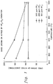
- FIG. 1 is a graph illustrating the thickness of an oxide layer, formed on top of a silicon nitride layer by oxidation of the silicon nitride according to the present invention, versus oxidation temperature (°C) for three different concentrations of a fluorine-containing compound.
- the data for this particular graph are for the use of NF3 as the fluorine-containing compound in a mixture of argon and oxygen in a ratio of about 4:1 (argon:oxygen) using RTA with a reaction time of about 1 to 5 minutes (this data comes from the example discussed above).
- NF3 as the fluorine-containing compound in a mixture of argon and oxygen in a ratio of about 4:1 (argon:oxygen) using RTA with a reaction time of about 1 to 5 minutes
- the vertical axis shows the thickness of an oxide in Angstroms formed on the surface of a silicon nitride layer having a substantially flat topography and an initial thickness of about 176 nm (1760 Angstroms).
- the oxidation time for these data is not constant, but rather is determined by the time required to form an oxide of about 22.5 nm (about 225 Angstroms) on a silicon layer at the particular oxidation temperature and NF3 concentration shown in the graph (this was discussed in greater detail in the example above).
- concentration of NF3 increases or the temperature decreases below about 1000°C
- the thickness of the oxide grown on the silicon nitride layer increases relative to the oxide grown on the silicon layer. It is expected that both of these two trends will continue into higher concentration ranges and lower temperature ranges. Also, it is believed that these two trends will be followed with the use of other fluorine-containing compounds.
- the present invention is further illustrated in one specific application for the preferred embodiment given below.
- This application deals with the manufacture of a memory device and is provided for the purpose of further description--the details provided therein are not intended to limit the scope of the present invention. Rather, the present invention can be used with many other devices having different structures and formed by different sets of processing steps such as the oxidation of nitride spacers previously formed on the sides of a gate conductor.
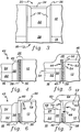
- FIG. 2 is a cut-away perspective view of a deep-trench memory storage cell 10 formed using a preferred embodiment of the present invention.
- the details of the structure and manufacture of this device are not critical to the practice of the present invention, but can be found in commonly-assigned U.S. patent number 4,801,988, issued January 31, 1989. All information believed necessary for the practice of the present invention is presented below.
- memory cell 10 is formed in an n-well 12 disposed in a silicon substrate 14 doped with a p-type dopant (i.e. a p+ substrate).
- a deep trench 16, used for storing charge corresponding to the memory contents of cell 10 is etched into substrate 14 through n-well 12.
- a p-channel transfer device 18 has a source/drain region 20 connected to a bit line 22 and another source/drain region 23 connected to trench 16 by a polysilicon surface strap 24.
- FIG. 3 is a cross-sectional view showing greater detail of the top portion of trench 16 of FIG. 2. The structure is illustrated just prior to gate oxide growth and gate polysilicon deposition.
- Trench 16 has a top end 25 which is connected to surface strap 24 through an opening therein (not shown).
- an ONO insulation layer 26 is formed on its interior surface.
- ONO layer 26 is a composite layer formed by first oxidizing the interior surface of trench 16 to form a 4 nm (40 Angstrom) silicon oxide layer, then forming a 9nm (90 Angstrom) silicon nitride layer, and finally subjecting this nitride layer to a 1000°C steam oxidation for 16 minutes to convert the top 2nm (20 Angstroms) of nitride to 3 nm (30 Angstroms) of oxide (these layers are not shown in FIG. 3, but are shown later in FIG. 4).
- trench 16 is filled with polysilicon and etched back partially to form a first polysilicon fill layer 28.
- An oxide layer is deposited overlying fill layer 28 and then etched back to form oxide collars 30.
- the top end of trench 16 is filled with polysilicon and then etched back about 200 nm (about 2000 Angstroms) to form a second polysilicon fill layer 32.
- a cap oxide layer 34 is formed on fill layer 32. It is planarized by polishing to a nitride layer (not shown) which has been formed over the n-well for this planarization. After polishing, the nitride is stripped using hot phosphoric acid. FIG. 3 shows the structure after this stripping.
- FIG. 4 is a cross-sectional view illustrating further detail of the top right-hand portion of trench 16 of FIG. 3.
- ONO insulation layer 26 is a composite layer having a first silicon oxide layer 36, a silicon nitride layer 38, and a second oxide layer 40.
- a thin oxide (not shown) which was under the nitride stop is etched using a dilute HF acid bath. This also removes a portion 42 of cap oxide layer 34, oxide collars 30, and oxide layer 40.
- FIG. 5 is a cross-sectional view of trench 16 of FIG. 4 where a gate oxide 46 and a polysilicon gate layer 48 have been formed without oxidation of silicon nitride, in contrast to the present invention.
- FIG. 5 illustrates the resulting topography for the trench where oxidation of the silicon nitride layer by the present invention is not used.
- a screen oxide (not shown) is grown for performing threshold tailoring ion implants and then stripped using dilute HF. As a result of this stripping, a portion 44 of silicon nitride layer 38 is exposed (i.e.
- cap oxide layer 34 As cap oxide layer 34, oxide collar 30, and oxide layer 40 are further etched back by the HF acid bath. Portion 44 has an extent of about 20 nm (about 200 Angstroms).
- gate oxide 46 is grown on n-well 12, and polysilicon gate layer 48 is deposited overlying gate oxide 46 and trench 16. Oxide layer 36 from FIG. 4 is shown as part of gate oxide layer 46.
- silicon nitride layer 38 is not oxidized during the growth of either the screen or gate oxide.
- polysilicon gate layer 48 extends downward into the top end of the trench such that portion 44 of silicon nitride layer 38 is disposed substantially between polysilicon layer 48 and n-well 12.
- Charge trapping at interface 50 may also occur during operation of the memory cell after manufacture which leads to a reliability problem.
- the silicon nitride layer disposed between polysilicon layer 48 and n-well 12 may be removed by oxidation according to the present invention so that parasitic device 52 is substantially eliminated.
- FIG. 6 is a cross-sectional view of trench 16 of FIG. 4 where a screen oxide 56 has been formed by oxidation of silicon nitride according to the present invention.
- FIG. 6 continues with the processing shown in FIG. 4 and makes use of the present invention to oxidize the top portion of the silicon nitride layer.
- screen oxide layer 56 is grown on n-well 12 for use during ion implantation and has a thickness of about 22.5 nm (about 225 Angstroms).
- Oxide layer 36 from FIG. 4 is shown as part of screen oxide layer 56.
- the top portion of silicon nitride layer 38 is oxidized to form a silicon oxide layer 60.
- Both the silicon and silicon nitride are oxidized in the same processing step using a mixture of oxygen and a fluorine-containing compound, preferably NF3, at processing conditions as described in detail above.
- An advantage of the present invention is that silicon corner 61 is rounded relative to what its shape would be in the absence of oxidation with a fluorine-containing compound.
- FIG. 7 is a cross-sectional view of trench 16 of FIG. 6 after a gate oxide 62 and a polysilicon gate layer 64 have been formed thereon.
- screen oxide 56 is stripped off.
- Gate oxide 62 is grown on the top surface 63 of n-well 12.
- Gate oxide 62 may be grown using an oxidizing mixture according to the present invention which will further oxidize a portion of silicon nitride layer 38.
- silicon nitride layer 38 is oxidized only during the growth of the screen oxide and not during the growth of the gate oxide.
- nitride layer 38 could be oxidized only during the growth of the gate oxide, or oxidized in two steps, first during the growth of the screen oxide and second during growth of the gate oxide as indicated above.
- a lower portion 66 of oxide layer 60 will typically extend below the top surface 68 of cap oxide layer 34, oxide collar 30, and oxide layer 40. This result occurs because the oxidizing mixture including the fluorine-containing compound partially diffuses into the top oxide layers and oxidizes portion 66 of oxide layer 60. In a typical device, for example, lower portion 66 may extend about 30 nm (about 300 Angstroms) below top surface 68. This result is significant because the removal of the screen oxide also removes about 20 nm (about 200 Angstroms) of the cap oxide. It is desirable to keep the gate polysilicon from over-lapping the un-oxidized nitride layer 38. Following the oxidation of the silicon nitride, substantially all the trapped charges are released into the surrounding oxide, and when the wafer is at a high temperature, are conducted to the substrate. Also, charging from later processing or other operations is not substantially trapped by oxide layer 60.
- polysilicon gate layer 64 is deposited thereover. It should be noted that, although polysilicon layer 64 still wraps around a top portion 70 of oxide layer 60 (which used to be silicon nitride layer 38), no parasitic leakage path is formed because oxide layer 60 does not substantially trap charges that reduce the threshold voltage of parasitic p-channel device 72 (which would occur if silicon nitride were not oxidized according to the present invention).
- processing continues in a conventional manner. This includes etching the polysilicon layer, implanting the junctions for devices in the memory cell, forming the surface strap, and forming passivation.
- an oxidizing mixture according to the present invention can be used to oxidize the nitride layer in a trench cell after the first polysilicon fill layer is formed, but before formation of the oxide collar. This requires the use of a wet or dry oxide etch to remove from the exposed surface of the first polysilicon fill layer.
- the oxidation of silicon nitride can provide more flexibility in adjusting the physical dimensions of a device.
- a silicon nitride layer is used as a structural element in a device because of an advantageous material property of the nitride.
- silicon nitride spacers are sometimes used for spacing the ion implants into the source/drain regions on the device.
- the dimensions of the initial silicon nitride layer for example an implant spacer, are increased. This increase in size can be varied to adjust the spacing of the implants for the lightly-doped drain device.
- the present invention is useful where it is desired to remove silicon nitride in an isotropic manner.
- "Kooi" type defects typically occur when forming semi-recessed oxide (SROX) isolation due to nitridization of silicon.
- SROX semi-recessed oxide
- these defects can be avoided in certain cases by forming the SROX using the oxidizing mixture of the present invention.
Landscapes
- Formation Of Insulating Films (AREA)
- Semiconductor Memories (AREA)
- Non-Volatile Memory (AREA)
Applications Claiming Priority (2)
| Application Number | Priority Date | Filing Date | Title |
|---|---|---|---|
| US54112 | 1993-04-27 | ||
| US08/054,112 US5434109A (en) | 1993-04-27 | 1993-04-27 | Oxidation of silicon nitride in semiconductor devices |
Publications (3)
| Publication Number | Publication Date |
|---|---|
| EP0624899A2 true EP0624899A2 (de) | 1994-11-17 |
| EP0624899A3 EP0624899A3 (de) | 1996-04-10 |
| EP0624899B1 EP0624899B1 (de) | 2000-08-16 |
Family
ID=21988885
Family Applications (1)
| Application Number | Title | Priority Date | Filing Date |
|---|---|---|---|
| EP94104574A Expired - Lifetime EP0624899B1 (de) | 1993-04-27 | 1994-03-23 | Oxidation von Silizium-Nitrid in der Herstellung von Halbleitenden Anordnungen |
Country Status (5)
| Country | Link |
|---|---|
| US (1) | US5434109A (de) |
| EP (1) | EP0624899B1 (de) |
| JP (1) | JP2607834B2 (de) |
| KR (1) | KR0122513B1 (de) |
| DE (1) | DE69425527T2 (de) |
Cited By (3)
| Publication number | Priority date | Publication date | Assignee | Title |
|---|---|---|---|---|
| WO1999012196A1 (en) * | 1997-09-04 | 1999-03-11 | Applied Materials, Inc. | Control of semiconductor device isolation properties through incorporation of fluorine in peteos films |
| EP0928023A1 (de) * | 1997-12-30 | 1999-07-07 | Siemens Aktiengesellschaft | Flache Grabenisolationsstruktur mit einem versenkten Nitridbelag, und Verfahren zur Herstellung derselben |
| WO2000024055A1 (en) | 1998-10-21 | 2000-04-27 | Advanced Micro Devices, Inc. | A semiconductor topography employing a nitrogenated shallow trench isolation structure |
Families Citing this family (56)
| Publication number | Priority date | Publication date | Assignee | Title |
|---|---|---|---|---|
| JP3590416B2 (ja) * | 1993-11-29 | 2004-11-17 | アネルバ株式会社 | 薄膜形成方法および薄膜形成装置 |
| TW236710B (de) * | 1994-04-08 | 1994-12-21 | ||
| JP3660391B2 (ja) * | 1994-05-27 | 2005-06-15 | 株式会社東芝 | 半導体装置の製造方法 |
| JP2630257B2 (ja) * | 1994-06-03 | 1997-07-16 | 日本電気株式会社 | 半導体装置の製造方法 |
| JP3304621B2 (ja) * | 1994-07-29 | 2002-07-22 | 三菱電機株式会社 | 半導体装置の製造方法 |
| US6207494B1 (en) * | 1994-12-29 | 2001-03-27 | Infineon Technologies Corporation | Isolation collar nitride liner for DRAM process improvement |
| JP2701795B2 (ja) * | 1995-06-28 | 1998-01-21 | 日本電気株式会社 | プロセスシミュレーション方法 |
| US5966595A (en) * | 1995-10-05 | 1999-10-12 | Micron Technology, Inc. | Method to form a DRAM capacitor using low temperature reoxidation |
| US5869405A (en) | 1996-01-03 | 1999-02-09 | Micron Technology, Inc. | In situ rapid thermal etch and rapid thermal oxidation |
| US5738909A (en) * | 1996-01-10 | 1998-04-14 | Micron Technology, Inc. | Method of forming high-integrity ultrathin oxides |
| US5843239A (en) * | 1997-03-03 | 1998-12-01 | Applied Materials, Inc. | Two-step process for cleaning a substrate processing chamber |
| US6057216A (en) * | 1997-12-09 | 2000-05-02 | International Business Machines Corporation | Low temperature diffusion process for dopant concentration enhancement |
| US6190955B1 (en) | 1998-01-27 | 2001-02-20 | International Business Machines Corporation | Fabrication of trench capacitors using disposable hard mask |
| US6033998A (en) * | 1998-03-09 | 2000-03-07 | Lsi Logic Corporation | Method of forming variable thickness gate dielectrics |
| US6201276B1 (en) * | 1998-07-14 | 2001-03-13 | Micron Technology, Inc. | Method of fabricating semiconductor devices utilizing in situ passivation of dielectric thin films |
| US6194736B1 (en) | 1998-12-17 | 2001-02-27 | International Business Machines Corporation | Quantum conductive recrystallization barrier layers |
| US6259129B1 (en) | 1999-04-20 | 2001-07-10 | International Business Machines Corporation | Strap with intrinsically conductive barrier |
| US6236077B1 (en) | 1999-04-20 | 2001-05-22 | International Business Machines Corporation | Trench electrode with intermediate conductive barrier layer |
| US6521529B1 (en) * | 2000-10-05 | 2003-02-18 | Advanced Micro Devices, Inc. | HDP treatment for reduced nickel silicide bridging |
| JP2003017595A (ja) * | 2001-06-29 | 2003-01-17 | Toshiba Corp | 半導体装置 |
| US6458650B1 (en) | 2001-07-20 | 2002-10-01 | Taiwan Semiconductor Manufacturing Company | CU second electrode process with in situ ashing and oxidation process |
| US6451662B1 (en) * | 2001-10-04 | 2002-09-17 | International Business Machines Corporation | Method of forming low-leakage on-chip capacitor |
| US6562491B1 (en) | 2001-10-15 | 2003-05-13 | Advanced Micro Devices, Inc. | Preparation of composite high-K dielectrics |
| US6559014B1 (en) | 2001-10-15 | 2003-05-06 | Advanced Micro Devices, Inc. | Preparation of composite high-K / standard-K dielectrics for semiconductor devices |
| US7115469B1 (en) | 2001-12-17 | 2006-10-03 | Spansion, Llc | Integrated ONO processing for semiconductor devices using in-situ steam generation (ISSG) process |
| US6790755B2 (en) | 2001-12-27 | 2004-09-14 | Advanced Micro Devices, Inc. | Preparation of stack high-K gate dielectrics with nitrided layer |
| US6589843B1 (en) | 2002-01-09 | 2003-07-08 | Micron Technology, Inc. | Methods of forming FLASH field effect transistor gates and non-FLASH field effect transistor gates |
| US6706576B1 (en) * | 2002-03-14 | 2004-03-16 | Advanced Micro Devices, Inc. | Laser thermal annealing of silicon nitride for increased density and etch selectivity |
| US7001814B1 (en) * | 2003-05-16 | 2006-02-21 | Advanced Micro Devices, Inc. | Laser thermal annealing methods for flash memory devices |
| US8581308B2 (en) * | 2004-02-19 | 2013-11-12 | Rochester Institute Of Technology | High temperature embedded charge devices and methods thereof |
| US20060084268A1 (en) * | 2004-10-15 | 2006-04-20 | Martin Verhoeven | Method for production of charge-trapping memory cells |
| JP2007165733A (ja) * | 2005-12-16 | 2007-06-28 | Elpida Memory Inc | 半導体装置及びその製造方法 |
| US8119538B1 (en) * | 2007-08-09 | 2012-02-21 | Cypress Semiconductor Corporation | Oxide formation in a plasma process |
| US9406574B1 (en) | 2007-08-09 | 2016-08-02 | Cypress Semiconductor Corporation | Oxide formation in a plasma process |
| US8980382B2 (en) | 2009-12-02 | 2015-03-17 | Applied Materials, Inc. | Oxygen-doping for non-carbon radical-component CVD films |
| US8741788B2 (en) | 2009-08-06 | 2014-06-03 | Applied Materials, Inc. | Formation of silicon oxide using non-carbon flowable CVD processes |
| US8449942B2 (en) * | 2009-11-12 | 2013-05-28 | Applied Materials, Inc. | Methods of curing non-carbon flowable CVD films |
| CN102687252A (zh) * | 2009-12-30 | 2012-09-19 | 应用材料公司 | 以可变的氮/氢比所制造的自由基来生长介电薄膜的方法 |
| JP2013517616A (ja) | 2010-01-06 | 2013-05-16 | アプライド マテリアルズ インコーポレイテッド | 酸化物ライナを使用する流動可能な誘電体 |
| CN102844848A (zh) | 2010-03-05 | 2012-12-26 | 应用材料公司 | 通过自由基成分化学气相沉积的共形层 |
| US9285168B2 (en) | 2010-10-05 | 2016-03-15 | Applied Materials, Inc. | Module for ozone cure and post-cure moisture treatment |
| US8664127B2 (en) | 2010-10-15 | 2014-03-04 | Applied Materials, Inc. | Two silicon-containing precursors for gapfill enhancing dielectric liner |
| US10283321B2 (en) | 2011-01-18 | 2019-05-07 | Applied Materials, Inc. | Semiconductor processing system and methods using capacitively coupled plasma |
| US8450191B2 (en) | 2011-01-24 | 2013-05-28 | Applied Materials, Inc. | Polysilicon films by HDP-CVD |
| US8716154B2 (en) | 2011-03-04 | 2014-05-06 | Applied Materials, Inc. | Reduced pattern loading using silicon oxide multi-layers |
| US8445078B2 (en) | 2011-04-20 | 2013-05-21 | Applied Materials, Inc. | Low temperature silicon oxide conversion |
| US8466073B2 (en) | 2011-06-03 | 2013-06-18 | Applied Materials, Inc. | Capping layer for reduced outgassing |
| US9404178B2 (en) | 2011-07-15 | 2016-08-02 | Applied Materials, Inc. | Surface treatment and deposition for reduced outgassing |
| US8617989B2 (en) | 2011-09-26 | 2013-12-31 | Applied Materials, Inc. | Liner property improvement |
| US8551891B2 (en) | 2011-10-04 | 2013-10-08 | Applied Materials, Inc. | Remote plasma burn-in |
| US8889566B2 (en) | 2012-09-11 | 2014-11-18 | Applied Materials, Inc. | Low cost flowable dielectric films |
| US9018108B2 (en) | 2013-01-25 | 2015-04-28 | Applied Materials, Inc. | Low shrinkage dielectric films |
| US9412581B2 (en) | 2014-07-16 | 2016-08-09 | Applied Materials, Inc. | Low-K dielectric gapfill by flowable deposition |
| US10020314B1 (en) | 2017-03-02 | 2018-07-10 | Sandisk Technologies Llc | Forming memory cell film in stack opening |
| US10847651B2 (en) | 2018-07-18 | 2020-11-24 | Micron Technology, Inc. | Semiconductor devices including electrically conductive contacts and related systems and methods |
| CN114639602B (zh) * | 2020-12-15 | 2026-03-27 | 东京毅力科创株式会社 | 蚀刻方法和蚀刻装置 |
Family Cites Families (7)
| Publication number | Priority date | Publication date | Assignee | Title |
|---|---|---|---|---|
| US4833094A (en) * | 1986-10-17 | 1989-05-23 | International Business Machines Corporation | Method of making a dynamic ram cell having shared trench storage capacitor with sidewall-defined bridge contacts and gate electrodes |
| US4801988A (en) * | 1986-10-31 | 1989-01-31 | International Business Machines Corporation | Semiconductor trench capacitor cell with merged isolation and node trench construction |
| US4748131A (en) * | 1987-02-06 | 1988-05-31 | The Aerospace Corporation | Method for increasing radiation hardness of MOS gate oxides |
| DE68916988T2 (de) * | 1988-03-16 | 1995-03-16 | Mitsui Toatsu Chemicals | Verfahren zur Herstellung von gasförmigen Fluoriden. |
| US5043224A (en) * | 1988-05-12 | 1991-08-27 | Lehigh University | Chemically enhanced thermal oxidation and nitridation of silicon and products thereof |
| US4894352A (en) * | 1988-10-26 | 1990-01-16 | Texas Instruments Inc. | Deposition of silicon-containing films using organosilicon compounds and nitrogen trifluoride |
| US5279705A (en) * | 1990-11-28 | 1994-01-18 | Dainippon Screen Mfg. Co., Ltd. | Gaseous process for selectively removing silicon nitride film |
-
1993
- 1993-04-27 US US08/054,112 patent/US5434109A/en not_active Expired - Fee Related
-
1994
- 1994-02-10 JP JP6036353A patent/JP2607834B2/ja not_active Expired - Lifetime
- 1994-03-23 EP EP94104574A patent/EP0624899B1/de not_active Expired - Lifetime
- 1994-03-23 DE DE69425527T patent/DE69425527T2/de not_active Expired - Fee Related
- 1994-03-25 KR KR1019940006032A patent/KR0122513B1/ko not_active Expired - Fee Related
Cited By (6)
| Publication number | Priority date | Publication date | Assignee | Title |
|---|---|---|---|---|
| WO1999012196A1 (en) * | 1997-09-04 | 1999-03-11 | Applied Materials, Inc. | Control of semiconductor device isolation properties through incorporation of fluorine in peteos films |
| US6451686B1 (en) | 1997-09-04 | 2002-09-17 | Applied Materials, Inc. | Control of semiconductor device isolation properties through incorporation of fluorine in peteos films |
| EP0928023A1 (de) * | 1997-12-30 | 1999-07-07 | Siemens Aktiengesellschaft | Flache Grabenisolationsstruktur mit einem versenkten Nitridbelag, und Verfahren zur Herstellung derselben |
| US6960818B1 (en) | 1997-12-30 | 2005-11-01 | Siemens Aktiengesellschaft | Recessed shallow trench isolation structure nitride liner and method for making same |
| WO2000024055A1 (en) | 1998-10-21 | 2000-04-27 | Advanced Micro Devices, Inc. | A semiconductor topography employing a nitrogenated shallow trench isolation structure |
| US6218720B1 (en) | 1998-10-21 | 2001-04-17 | Advanced Micro Devices, Inc. | Semiconductor topography employing a nitrogenated shallow trench isolation structure |
Also Published As
| Publication number | Publication date |
|---|---|
| JPH06314777A (ja) | 1994-11-08 |
| EP0624899A3 (de) | 1996-04-10 |
| DE69425527T2 (de) | 2001-04-26 |
| US5434109A (en) | 1995-07-18 |
| DE69425527D1 (de) | 2000-09-21 |
| KR0122513B1 (ko) | 1997-11-26 |
| EP0624899B1 (de) | 2000-08-16 |
| JP2607834B2 (ja) | 1997-05-07 |
Similar Documents
| Publication | Publication Date | Title |
|---|---|---|
| EP0624899B1 (de) | Oxidation von Silizium-Nitrid in der Herstellung von Halbleitenden Anordnungen | |
| EP0690487B1 (de) | Verfahren zur Herstellung von Oxydschichten | |
| US5296411A (en) | Method for achieving an ultra-reliable thin oxide using a nitrogen anneal | |
| EP0696051B1 (de) | Verfahren zur Herstellung einer Oxidschicht in der Halbleitertechnik | |
| US6190973B1 (en) | Method of fabricating a high quality thin oxide | |
| EP1051744B1 (de) | Verfahren zur herstellung eines halbleiterbauelements | |
| US6664160B2 (en) | Gate structure with high K dielectric | |
| US6228779B1 (en) | Ultra thin oxynitride and nitride/oxide stacked gate dielectrics fabricated by high pressure technology | |
| US20070169696A1 (en) | Two-step post nitridation annealing for lower eot plasma nitrided gate dielectrics | |
| US8227356B2 (en) | Method of forming semiconductor device and semiconductor device | |
| US6953727B2 (en) | Manufacture method of semiconductor device with gate insulating films of different thickness | |
| US6225171B1 (en) | Shallow trench isolation process for reduced for junction leakage | |
| US6184155B1 (en) | Method for forming a ultra-thin gate insulator layer | |
| EP0595464A2 (de) | Verfahren zum Aufwachsen von Oxidschichten in einem Verfahren zur Herstellung eines integrierten Schaltkreises | |
| US7157339B2 (en) | Method for fabricating semiconductor devices having dual gate oxide layers | |
| WO2000034548A1 (en) | Multiple-thickness gate oxide formed by oxygen implantation | |
| US5202280A (en) | Method for fabricating a semiconductor device | |
| US20020177327A1 (en) | Method for forming a gate dielectric layer by a single wafer process | |
| KR100235962B1 (ko) | 초저접합을 갖는 반도체소자 제조방법 | |
| KR960008903B1 (ko) | 반도체 기판상의 유전체막 형성방법 | |
| KR20020045266A (ko) | 커패시터의 유전체막 형성 방법 | |
| JPH08241991A (ja) | 半導体装置の製造方法 |
Legal Events
| Date | Code | Title | Description |
|---|---|---|---|
| PUAI | Public reference made under article 153(3) epc to a published international application that has entered the european phase |
Free format text: ORIGINAL CODE: 0009012 |
|
| AK | Designated contracting states |
Kind code of ref document: A2 Designated state(s): DE FR GB |
|
| 17P | Request for examination filed |
Effective date: 19950227 |
|
| PUAL | Search report despatched |
Free format text: ORIGINAL CODE: 0009013 |
|
| AK | Designated contracting states |
Kind code of ref document: A3 Designated state(s): DE FR GB |
|
| 17Q | First examination report despatched |
Effective date: 19971030 |
|
| GRAG | Despatch of communication of intention to grant |
Free format text: ORIGINAL CODE: EPIDOS AGRA |
|
| GRAG | Despatch of communication of intention to grant |
Free format text: ORIGINAL CODE: EPIDOS AGRA |
|
| GRAH | Despatch of communication of intention to grant a patent |
Free format text: ORIGINAL CODE: EPIDOS IGRA |
|
| GRAH | Despatch of communication of intention to grant a patent |
Free format text: ORIGINAL CODE: EPIDOS IGRA |
|
| GRAA | (expected) grant |
Free format text: ORIGINAL CODE: 0009210 |
|
| AK | Designated contracting states |
Kind code of ref document: B1 Designated state(s): DE FR GB |
|
| REF | Corresponds to: |
Ref document number: 69425527 Country of ref document: DE Date of ref document: 20000921 |
|
| ET | Fr: translation filed | ||
| PGFP | Annual fee paid to national office [announced via postgrant information from national office to epo] |
Ref country code: FR Payment date: 20010312 Year of fee payment: 8 |
|
| PG25 | Lapsed in a contracting state [announced via postgrant information from national office to epo] |
Ref country code: GB Free format text: LAPSE BECAUSE OF NON-PAYMENT OF DUE FEES Effective date: 20010323 |
|
| PLBE | No opposition filed within time limit |
Free format text: ORIGINAL CODE: 0009261 |
|
| STAA | Information on the status of an ep patent application or granted ep patent |
Free format text: STATUS: NO OPPOSITION FILED WITHIN TIME LIMIT |
|
| 26N | No opposition filed | ||
| GBPC | Gb: european patent ceased through non-payment of renewal fee |
Effective date: 20010323 |
|
| PG25 | Lapsed in a contracting state [announced via postgrant information from national office to epo] |
Ref country code: FR Free format text: LAPSE BECAUSE OF NON-PAYMENT OF DUE FEES Effective date: 20021129 |
|
| REG | Reference to a national code |
Ref country code: FR Ref legal event code: ST |
|
| PGFP | Annual fee paid to national office [announced via postgrant information from national office to epo] |
Ref country code: DE Payment date: 20030325 Year of fee payment: 10 |
|
| PG25 | Lapsed in a contracting state [announced via postgrant information from national office to epo] |
Ref country code: DE Free format text: LAPSE BECAUSE OF NON-PAYMENT OF DUE FEES Effective date: 20041001 |