EP0624960A2 - Procédé et dipositif pour donner une réponse linéaire en fréquence à un signal - Google Patents
Procédé et dipositif pour donner une réponse linéaire en fréquence à un signal Download PDFInfo
- Publication number
- EP0624960A2 EP0624960A2 EP94303044A EP94303044A EP0624960A2 EP 0624960 A2 EP0624960 A2 EP 0624960A2 EP 94303044 A EP94303044 A EP 94303044A EP 94303044 A EP94303044 A EP 94303044A EP 0624960 A2 EP0624960 A2 EP 0624960A2
- Authority
- EP
- European Patent Office
- Prior art keywords
- signal
- path
- signal path
- delay element
- putting
- Prior art date
- Legal status (The legal status is an assumption and is not a legal conclusion. Google has not performed a legal analysis and makes no representation as to the accuracy of the status listed.)
- Withdrawn
Links
- 238000000034 method Methods 0.000 title claims abstract description 7
- 238000010587 phase diagram Methods 0.000 description 6
- 238000010586 diagram Methods 0.000 description 5
- 241001644893 Entandrophragma utile Species 0.000 description 2
- 239000004020 conductor Substances 0.000 description 2
- 230000002411 adverse Effects 0.000 description 1
- 230000000694 effects Effects 0.000 description 1
Images



Classifications
-
- H—ELECTRICITY
- H04—ELECTRIC COMMUNICATION TECHNIQUE
- H04B—TRANSMISSION
- H04B3/00—Line transmission systems
- H04B3/02—Details
- H04B3/04—Control of transmission; Equalising
- H04B3/14—Control of transmission; Equalising characterised by the equalising network used
Definitions
- the present invention relates to electric circuit design in general, and more particularly, to methods and apparatus which have a sloped frequency response.
- Embodiments of the present invention are capable of imparting a sloped linear frequency response to a signal while avoiding many of the costs and restrictions associated with prior methods. Specifically, embodiments of the present invention can be used in conjunction with utile circuits to correct the sloped frequency response characteristic of the utile circuit. Furthermore, embodiments of the present invention need not change the nominal phase, the center band amplitude or the group delay of the signal.
- the first signal path advantageously comprises a first bi-phase attenuator
- the second signal path advantageously comprises a first delay element
- the third signal path advantageously comprises both a second bi-phase attenuator and a second delay element.
- the first delay element preferably makes the second signal path substantially close to 2 N + 1 8 ⁇ 0 seconds longer than the first signal path, where N is an integer and ⁇ 0 is the frequency of a sinusoidal component in the narrowband signal input to the embodiment.
- the second delay element preferably makes the third signal path substantially close to 2 N + 1 4 ⁇ 0 seconds longer than the first signal path.
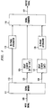
- FIG. 1 shows a block diagram of an illustrative embodiment of the present invention.
- FIG. 2 shows a block diagram of another illustrative embodiment of the present invention.
- FIG. 3 shows a block diagram of yet another illustrative embodiment of the present invention.
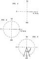
- FIG. 4 shows a phase diagram of a typical signal on lead 109 of the illustrative embodiment shown in FIG. 1.
- FIG. 5 shows a phase diagram of a typical signal on signal path 113, upon entering signal combiner 119, of the illustrative embodiment shown in FIG. 1.
- FIG. 6 shows a phase diagram of a typical signal on signal path 123, upon entering signal combiner 119, of the illustrative embodiment shown in FIG. 1.
- FIG. 7 shows a phase diagram of a typical signal on signal path 129, upon entering signal combiner 119, of the illustrative embodiment shown in FIG. 1.
- FIG. 8 shows a phase diagram of a typical signal on lead 121 of the illustrative embodiment shown in FIG. 1.
- FIG. 1 shows a block diagram of an illustrative embodiment of the present invention that advantageously comprises signal divider 111, signal combiner 129, delay element 125, delay element 131, bi-phase attenuator 115 and bi-phase attenuator 135.
- Signal divider 111 preferably receives, from lead 109, a narrowband input signal comprising: (1) a sinusoidal component at ⁇ 0 radians per second, (2) an RMS amplitude (hereinafter "amplitude" ) , and (3) a phase.
- Signal divider 111 preferably creates a first signal on signal path 113, a second signal on signal path 123 and a third signal on signal path 129 such that all three signals are analog representations of the input signal. While it is preferred that the first signal, the second signal and the third signal be created with equal amplitude and phase by signal divider 111, it will be clear to those skilled in the art how to make and use embodiments of the present invention in which the first, second and/or third signals are not created with equal amplitude or phase.
- signal divider 111 can be easily fabricated (using e.g., a Wilkinson power divider, a hybrid coupler, etc.) or purchased commercially. See E.J. Wilkinson, “An N Way Hybrid Power Divider,” IRE Trans., MTT-8, 116118 (Jan. 1960); and J. Lange, “Integrated Stripline Quadrature Hybrid,” MTT-17 , No. 12, 1150- 1151 (Dec. 1969). Likewise, it will be clear to those skilled in the art that signal divider 111 can be fabricated as two, one-to-two dividers as illustrated at 311 and 315 in FIG. 3.
- Signal combiner 119 advantageously receives as input the first signal from signal path 113, the second signal from signal path 123 and the third signal from signal path 129, and preferably creates an output signal, on lead 121, based on the unweighted sum of the three input signals. While it is preferred that signal combiner 119 add the first signal, the second signal and the third signal in phase, it will be clear to those skilled in the art how to make and use embodiments of the present invention in which the respective input signals are disproportionately added and/or are not added in phase. Furthermore, it will be clear to those skilled in the art that signal combiner 119 can be easily fabricated (using e.g., a Wilkinson power divider, a hybrid coupler, etc.) or purchased commercially. See E.J.
- signal combiner 119 can be fabricated as two, two-to-one signal combiners, as illustrated at 319 and 327 in FIG. 3.
- Delay element 125 is preferably a length of conducting material (e.g., coaxial cable, a section of strip line, a microstrip, a lumped delay line, etc.) lying in signal path 123 that causes signal path 123 to be substantially close to 2 N + 1 8 ⁇ 0 seconds longer than signal path 113, where N is an integer.
- the purpose of delay element 125 is to impart a group delay to the second signal on signal path 123 such that the phase of the sinusoidal component on signal path 123 is shifted by either 90 ° or 270 ° (depending on whether a positive frequency response slope or a negative frequency response slope is desired) relative to the phase of the sinusoidal component on signal path 113.
- delay element 125 Given the purpose of delay element 125, it will be clear to those skilled in the art that delay element 125 can be subsumed within signal divider 111. Likewise, it will be clear to those skilled in the art that delay element 125 can be subsumed into signal combiner 119.
- Delay element 131 is preferably a length of conducting material (e.g., coaxial cable, a section of strip line, a microstrip, a lumped delay line, etc.) lying in signal path 129 that causes signal path 129 to be substantially close to 2 N + 1 4 ⁇ 0 seconds longer than signal path 113, where N is an integer.
- the purpose of delay element 131 is to impart a group delay to the third signal on signal path 131 such that the phase of the sinusoidal component on signal path 131 is shifted by 180 ° relative to the phase of the sinusoidal component on signal path 113.
- delay element 129 can be subsumed within signal divider 111.
- delay element 129 can be subsumed into signal combiner 119.
- a first signal control block such as bi-phase attenuator 115, lies in signal path 113 and advantageously multiplies a signal placed on its input by a factor denoted G 1.
- a second signal control block such as bi-phase attenuator 135, lies in signal path 129 and advantageously multiplies a signal placed on its input by a factor denoted G 2.
- the factor G 1 preferably is within the range - 1 ⁇ G 1 ⁇ + 1, and the factor G 2 is preferably within the range -1 ⁇ G 2 ⁇ + 1.
- bi-phase attenuator 115 and bi-phase attenuator 135 be equal although it will be clear to those skilled in the art how to make and use embodiments of the present invention in which they are not. It will be clear to those skilled in the art that bi-phase attenuator 115 and bi-phase attenuator 135 can be easily fabricated or purchased commercially. Furthermore, it will be clear to those skilled in the art that either or both of bi-phase attenuator 115 and bi-phase attenuator 135 can be subsumed into signal divider 111 or signal combiner 119.
- FIG. 2 and FIG. 3 Block diagrams portraying other illustrative embodiments of the present invention are shown in FIG. 2 and FIG. 3. It will be clear to those skilled in the art how to make and use embodiments of the present invention in accordance with FIG. 2 and FIG. 3 from the same components described for the embodiment of FIG. 1.
- FIG. 4 shows a narrowband signal, on lead 109, which comprises three sinusoidal components, ⁇ L , ⁇ 0, and ⁇ H , all illustratively of the same amplitude and identical phase.
- ⁇ L is of a lower frequency that ⁇ 0 and ⁇ 0 is of a lower frequency than ⁇ H .
- FIG. 5 illustrates the phase and magnitude relationship of ⁇ L , ⁇ 0, and ⁇ H on signal path 113, upon entering signal combiner 119, with respect to the magnitude and phase of the signals on signal path 123 and signal path 129.
- FIG. 6 illustrates the phase and magnitude relationship of ⁇ L , ⁇ 0, and ⁇ H on signal path 123, upon entering signal combiner 119, with respect to the magnitude and phase of the signals on signal path 113 and signal path 129. While the magnitude of ⁇ L , ⁇ 0 and ⁇ H upon entering signal combiner 119 are the same, the phases are different due to the group delay in signal path 123 (including delay element 125).
- FIG. 7 illustrates the phase and magnitude relationship of ( ⁇ L , ⁇ 0, and ⁇ H on signal path 129, upon entering signal combiner 119, with respect to the magnitude and phase of the signals on signal path 113 and signal path 123. While the magnitude of ⁇ L , ⁇ 0, and ⁇ H upon entering signal combiner 119 are the same, the phases are different due to the group delay in signal path 123 (including delay element 131).
- FIG. 8 illustrates the phase and magnitude relationship of ⁇ L , ⁇ 0, and ⁇ H on lead 121 after signal combiner 119 has added the three signals.
Landscapes
- Engineering & Computer Science (AREA)
- Computer Networks & Wireless Communication (AREA)
- Signal Processing (AREA)
- Transmitters (AREA)
- Noise Elimination (AREA)
- Stabilization Of Oscillater, Synchronisation, Frequency Synthesizers (AREA)
Applications Claiming Priority (2)
| Application Number | Priority Date | Filing Date | Title |
|---|---|---|---|
| US08/059,798 US5311155A (en) | 1993-05-10 | 1993-05-10 | Method and apparatus for imparting a linear frequency response to a signal |
| US59798 | 1998-04-14 |
Publications (2)
| Publication Number | Publication Date |
|---|---|
| EP0624960A2 true EP0624960A2 (fr) | 1994-11-17 |
| EP0624960A3 EP0624960A3 (fr) | 1996-04-10 |
Family
ID=22025308
Family Applications (1)
| Application Number | Title | Priority Date | Filing Date |
|---|---|---|---|
| EP94303044A Withdrawn EP0624960A3 (fr) | 1993-05-10 | 1994-04-27 | Procédé et dipositif pour donner une réponse linéaire en fréquence à un signal. |
Country Status (4)
| Country | Link |
|---|---|
| US (1) | US5311155A (fr) |
| EP (1) | EP0624960A3 (fr) |
| JP (1) | JP2892279B2 (fr) |
| KR (1) | KR940027291A (fr) |
Families Citing this family (6)
| Publication number | Priority date | Publication date | Assignee | Title |
|---|---|---|---|---|
| JPH0846459A (ja) * | 1994-07-26 | 1996-02-16 | Mitsubishi Electric Corp | マイクロ波増幅器回路 |
| US5506549A (en) * | 1994-11-14 | 1996-04-09 | Dsc Communications Corporation | Cable equalizer |
| US5576671A (en) * | 1995-04-24 | 1996-11-19 | Motorola, Inc. | Method and apparatus for power combining/dividing |
| US6856215B2 (en) * | 2001-08-24 | 2005-02-15 | Powerwave Technologies, Inc. | System and method for adjusting group delay |
| US7049907B2 (en) * | 2001-08-24 | 2006-05-23 | Powerwave Technologies, Inc. | System and method for adjusting group delay |
| US8503952B2 (en) * | 2008-04-10 | 2013-08-06 | Broadcom Corporation | Compensation of an asymmetric frequency response of a radio |
Family Cites Families (6)
| Publication number | Priority date | Publication date | Assignee | Title |
|---|---|---|---|---|
| SE355913B (fr) * | 1967-03-16 | 1973-05-07 | Fujitsu Ltd | |
| FR2415923A2 (fr) * | 1978-01-25 | 1979-08-24 | Cit Alcatel | Procede de compensation du bruit d'intermodulation et dispositifs pour sa mise en oeuvre |
| US4580105A (en) * | 1985-01-25 | 1986-04-01 | At&T Bell Laboratories | Automatic reduction of intermodulation products in high power linear amplifiers |
| AU583222B2 (en) * | 1985-08-20 | 1989-04-20 | Mitsubishi Denki Kabushiki Kaisha | Equalizer and equalizing circuit using the same |
| US5109793A (en) * | 1990-03-26 | 1992-05-05 | Ballejos Paul J | Painting shield apparatus for windows |
| US5223808A (en) * | 1992-02-25 | 1993-06-29 | Hughes Aircraft Company | Planar ferrite phase shifter |
-
1993
- 1993-05-10 US US08/059,798 patent/US5311155A/en not_active Expired - Lifetime
-
1994
- 1994-04-27 EP EP94303044A patent/EP0624960A3/fr not_active Withdrawn
- 1994-05-09 KR KR1019940010050A patent/KR940027291A/ko not_active Abandoned
- 1994-05-09 JP JP6117405A patent/JP2892279B2/ja not_active Expired - Lifetime
Also Published As
| Publication number | Publication date |
|---|---|
| US5311155A (en) | 1994-05-10 |
| KR940027291A (ko) | 1994-12-10 |
| EP0624960A3 (fr) | 1996-04-10 |
| JPH07321680A (ja) | 1995-12-08 |
| JP2892279B2 (ja) | 1999-05-17 |
Similar Documents
| Publication | Publication Date | Title |
|---|---|---|
| US5304945A (en) | Low-distortion feed-forward amplifier | |
| EP0286390B1 (fr) | Amplificateur micro-ondes à FET à combinaison de puissance | |
| EP0540286B1 (fr) | Circuit de combinaison de distribution de puissance à haute fréquence | |
| JPH07263993A (ja) | 電力合成器/分割器 | |
| JPS63198408A (ja) | バイアス回路 | |
| CN1116736C (zh) | 用于减小电路产生的失真的控制系统的双边带导频技术 | |
| EP0624960A2 (fr) | Procédé et dipositif pour donner une réponse linéaire en fréquence à un signal | |
| US7295090B2 (en) | Filter circuit | |
| US4348642A (en) | Feedforward wideband amplifier | |
| US5291156A (en) | Method and apparatus for imparting positive phase slope to a narrowband signal | |
| Lau et al. | Simplified design technique for high-performance microstrip multisection couplers | |
| US5585769A (en) | Passive temperature variable phase-shifter | |
| US20050275483A1 (en) | Method of combining signals and device therefor | |
| US4638261A (en) | Low noise amplifier with high intercept point | |
| JPS5925401A (ja) | 抵抗減衰器 | |
| JPS61198801A (ja) | マイクロ波可変減衰器 | |
| US3629740A (en) | Transmission line filter circuit | |
| KR100214454B1 (ko) | 고주파 상쇄회로 | |
| WO1995016267A2 (fr) | Circuit symetriseur resonnant a rapport arbitraire de transformation d'impedance | |
| JPH06216671A (ja) | 高周波増幅装置 | |
| US6219683B1 (en) | Radially distributed transverse filter | |
| Hollo et al. | EE406-MTU Radio Telescope Project Design and Fabrication of IF Section of Radio Receiver | |
| Lynch et al. | Third order intermodulation performance of above resonance circulators | |
| JPS5918728Y2 (ja) | 信号分岐回路 | |
| JP2005142724A (ja) | 移相器 |
Legal Events
| Date | Code | Title | Description |
|---|---|---|---|
| PUAI | Public reference made under article 153(3) epc to a published international application that has entered the european phase |
Free format text: ORIGINAL CODE: 0009012 |
|
| AK | Designated contracting states |
Kind code of ref document: A2 Designated state(s): DE FR GB IT |
|
| PUAL | Search report despatched |
Free format text: ORIGINAL CODE: 0009013 |
|
| AK | Designated contracting states |
Kind code of ref document: A3 Designated state(s): DE FR GB IT |
|
| 17P | Request for examination filed |
Effective date: 19960925 |
|
| 17Q | First examination report despatched |
Effective date: 20000711 |
|
| STAA | Information on the status of an ep patent application or granted ep patent |
Free format text: STATUS: THE APPLICATION IS DEEMED TO BE WITHDRAWN |
|
| 18D | Application deemed to be withdrawn |
Effective date: 20001122 |