EP0625836B1 - Verfahren und Anordnung zum Abzweigen und Einfügen von Digitalsignalen - Google Patents
Verfahren und Anordnung zum Abzweigen und Einfügen von Digitalsignalen Download PDFInfo
- Publication number
- EP0625836B1 EP0625836B1 EP94106997A EP94106997A EP0625836B1 EP 0625836 B1 EP0625836 B1 EP 0625836B1 EP 94106997 A EP94106997 A EP 94106997A EP 94106997 A EP94106997 A EP 94106997A EP 0625836 B1 EP0625836 B1 EP 0625836B1
- Authority
- EP
- European Patent Office
- Prior art keywords
- multiplex signal
- multiplex
- transformed
- multiplexer
- signal
- Prior art date
- Legal status (The legal status is an assumption and is not a legal conclusion. Google has not performed a legal analysis and makes no representation as to the accuracy of the status listed.)
- Expired - Lifetime
Links
- 238000000034 method Methods 0.000 title claims description 8
- 101100129649 Schizosaccharomyces pombe (strain 972 / ATCC 24843) mde2 gene Proteins 0.000 claims abstract description 14
- 101000630267 Homo sapiens Probable glutamate-tRNA ligase, mitochondrial Proteins 0.000 claims abstract description 13
- 101150090066 MDE1 gene Proteins 0.000 claims abstract description 13
- 102100026125 Probable glutamate-tRNA ligase, mitochondrial Human genes 0.000 claims abstract description 13
- 230000005540 biological transmission Effects 0.000 claims description 6
- 101000924530 Homo sapiens Protein arginine N-methyltransferase 5 Proteins 0.000 claims description 2
- 101000825632 Homo sapiens Spindle and kinetochore-associated protein 1 Proteins 0.000 claims description 2
- 102100034607 Protein arginine N-methyltransferase 5 Human genes 0.000 claims description 2
- 102100022915 Spindle and kinetochore-associated protein 1 Human genes 0.000 claims description 2
- 101000960946 Homo sapiens Interleukin-19 Proteins 0.000 claims 3
- 102100039879 Interleukin-19 Human genes 0.000 claims 3
- 238000011144 upstream manufacturing Methods 0.000 claims 2
- 230000001360 synchronised effect Effects 0.000 claims 1
- 230000002093 peripheral effect Effects 0.000 abstract 2
- 238000000605 extraction Methods 0.000 abstract 1
- 238000012966 insertion method Methods 0.000 abstract 1
- 238000010586 diagram Methods 0.000 description 6
- 238000003780 insertion Methods 0.000 description 6
- 230000037431 insertion Effects 0.000 description 6
- APCLRHPWFCQIMG-UHFFFAOYSA-N 4-(5,6-dimethoxy-1-benzothiophen-2-yl)-4-oxobutanoic acid Chemical compound C1=C(OC)C(OC)=CC2=C1SC(C(=O)CCC(O)=O)=C2 APCLRHPWFCQIMG-UHFFFAOYSA-N 0.000 description 2
- 101150092365 MSA2 gene Proteins 0.000 description 2
- 108010057081 Merozoite Surface Protein 1 Proteins 0.000 description 2
- 101100240989 Schizosaccharomyces pombe (strain 972 / ATCC 24843) nrd1 gene Proteins 0.000 description 2
- 230000000712 assembly Effects 0.000 description 2
- 238000000429 assembly Methods 0.000 description 2
- 239000002131 composite material Substances 0.000 description 2
- 230000003111 delayed effect Effects 0.000 description 2
- 208000020997 susceptibility to multiple system atrophy 1 Diseases 0.000 description 2
- 230000009466 transformation Effects 0.000 description 2
- 102100028043 Fibroblast growth factor 3 Human genes 0.000 description 1
- 108050002021 Integrator complex subunit 2 Proteins 0.000 description 1
- 238000005352 clarification Methods 0.000 description 1
- 238000004891 communication Methods 0.000 description 1
- 238000011161 development Methods 0.000 description 1
- 230000018109 developmental process Effects 0.000 description 1
- 230000006870 function Effects 0.000 description 1
- 239000000203 mixture Substances 0.000 description 1
- 238000012360 testing method Methods 0.000 description 1
Images



Classifications
-
- H—ELECTRICITY
- H04—ELECTRIC COMMUNICATION TECHNIQUE
- H04J—MULTIPLEX COMMUNICATION
- H04J3/00—Time-division multiplex systems
- H04J3/02—Details
- H04J3/08—Intermediate station arrangements, e.g. for branching, for tapping-off
Definitions
- the invention relates to a method for branching and inserting of digital signals according to the preamble of the claim 1 and a branch multiplexer according to the preamble of claim 4, as already known from EP-A-214783.
- connection modules Central control of the connection modules is also advantageous, which enables a high degree of flexibility.
- the invention is based on exemplary embodiments and timing diagrams explained in more detail.
- the branch multiplexer also contains the same second one Interface INTB, whose data input DE2 has a second multiplex signal MSE2 is fed. At its data output DA2 a corresponding multiplex signal MSA2 is emitted.
- the Data ports corresponding to the first interface are with PA2 and PE2.
- the first multiplex signal MSE1 be switched through completely the transformed multiplex signal MDE1 via the second shift register SR2 and the second multiplexer MUX2 to the input port PE2 of the second interface INTB switched through.
- the signal is then again converted into a standard Multiplex signal MSA2 implemented that the received corresponds to the first multiplex signal MSE1.
- the second multiplex signal MSE2 over the elastic Memory ES, the first multiplexer MUX1 and the input port PA2 fed to the first interface INTA and as a multiplex signal MSA1 switched through.
- those sent by the channel assemblies digital signals to be inserted EDSA1, ... in an odd Bus band position of the composite multiplex signal ZMS transmitted when sent out via the first interface INTA and in an even base time position bank code 2, 4, ..., if they are sent out via the second interface INTB.
- the one corresponding digital signal EDSB1 of this channel in the even number Bus time slot BZL 2 sends out that over the second Multiplexer MUX2 in the transmitted multiplex signal to be sent MDA2 inserted, transferred to the second interface INTB and sent out.
Landscapes
- Engineering & Computer Science (AREA)
- Computer Networks & Wireless Communication (AREA)
- Signal Processing (AREA)
- Time-Division Multiplex Systems (AREA)
- Data Exchanges In Wide-Area Networks (AREA)
Description
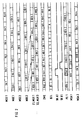
- Fig. 1
- ein Prinzipschaltbild des Abzweigmultiplexers
- Fig. 2
- ein zugehöriges Zeitdiagramm,
- Fig. 3
- eine Variante des Abzweigmultiplexers und
- Fig. 4
- ein zugehöriges Zeitdiagramm.
Claims (6)
- Verfahren zum Abzweigen und Einfügen von Digitalsignalen (DSA1, ... DSB1), die in Kanäle eines Multiplexsignals (MSE1, MSA1; MSE2, MSA2) übertragen werden,
dadurch gekennzeichnet,daß die ankommenden Multiplexsignale (MSE1, MSE2) wortweise in transformierte Multiplexsignale (MDE1, MDE2) umgesetzt werden, bei denen jeweils Datenwörtern mit verdoppelter Bitrate gleichlange Lücken folgen,daß ein transformiertes Multiplexsignal (MDE2) durch eine steuerbare Laufzeiteinrichtung (ES) auf das andere transformiterte Multiplexsignal (MDE1) synchronisiert wird,daß die abzuzweigenden Digitalsignale (DSA1, DSB1...) der zugehörigen Kanäle (KA1, KB1,...) jedes transformierten Multiplexsignals (MDE1, MDE2) einer ungeradzahligen oder einer geradzahligen Buszeitlage (BZL) zugeordnet werden und zu einem Zeitmultiplexsignal (ZME) zusammengefaßt allen Anschlußbaugruppen (KK1...KKn) zugeführt werden,daß die von den Anschlußbaugruppen (KK1...KKn) auszusenden Digitalsignalen (EDSA1, EDSB1...) für beide Übertragungsrichtungen gleichermaßen zu einem Zeitmultiplexsignal (ZMS) zusammengefaßt werden,daß jeweils ein einzufügendes Digitalsignal (EDSA1) in den zugehörigen Datenkanal (KA1) eines transformierten Multiplexsignals (MDA1) eingefügt und in ein normgerechtes Multiplexsignal (MSA1) umgesetzt wird. - Verfahren nach Anspruch 1,
dadurch gekennzeichnet,daß die abzuzweigenden Digitalsignale (ASA1, ADSB1) an die Anschlußbaugruppen (KK1, ...KKn) durchgeschaltet werden unddaß diese Steuersignale (SKA1, SKB1) erhalten. - Verfahren nach Anspruch 1,
dadurch gekennzeichnet,
daß die transformierten Multiplexsignale (MDE1, MDE2; MDA1, MDA2) seriell oder byteparallel übertragen werden. - Abzweigmultiplexer zum Abzweigen und Einfügen von Digitalsignalen, die in Kanälen (KA1, ...KB1,...) von Multiplexsignalen (MSE1, MSE2, MSA1, MSA2) übertragen werden,
dadurch gekennzeichnet,daß ein erstes Interface (INTA) vorgesehen ist mit einem ersten Dateneingang (DE1), dem ein erstes ankommendes Multiplexsignal (MSE1) zugeführt wird,
mit einem ersten Ausgangsport (PA1), an dem ein transformiertes Multiplexsignal (MDE1) abgegeben wird, dessen Datenwörter die doppelte Datenrate aufweisen und durch gleichlange Lücken getrennt sind, mit einem Eingangsport (PE1), dem ein gleich strukturiertes transformiertes Multiplexsignal (MSA1) zugeführt wird und einem ersten Datenausgang (DA1), an dem ein erstes abgehendes Multiplexsignal (MSA1) ausgesendet wird, daß ein zweites gleiches Interface (INTB) vorgesehen ist, mit einem Dateneingang (DE2) dem ein zweites Multiplexsignal (MSE2) zugeführt wird, mit einem Ausgangsport (PA2) an dem ein transformiertes zweites Mutliplexsignal (MDE2) abgegeben wird, mit einem Eingangsport (PE2), dem ein transformiertes zweites Multiplexsignal (MDA2) zugeführt wird und mit einem Datenausgang (DA2), an dem ein zweites Multiplexsignal (MSA2) ausgesendet wird,daß ein elastischer Speicher (ES) vorgesehen ist, der zwischen dem Ausgangsport (PA2) des zweiten Interface (INTB) und einem dem Eingangsport (PE1) des ersten Interface (INTA) vorgeschaltetem ersten Multiplexer (MUX1) eingeschaltet ist,daß die Ausgangsports (PA1, PA2) beider Interfaces (INTA, INTB) direkt oder über den elastischen Speicher (ES) auf einen dritten Multiplexer (MUX3) geführt sind, an dessen Ausgang ein Empfangsbus (BE) liegt, an den die Dateneingänge (DI) von Anschlußbaugruppen (KK1...KKn) angeschaltet sind, daß ein Sendebus (BS) vorgesehen ist, an den die Datenaugänge (DO) der Anschlußbaugruppen (KK1...KKn) angeschaltet sind,daß ein zweiter Multiplexer (MUX2) vorgesehen ist, an dessen Eingänge (E1, E2) der Ausgangsport (PA1) des ersten Interface (INTA) und der Sendebus (BS) geführt sind,daß Laufzeitglieder (SR2, SR1) jeweils einem Eingang (E1, E2) des zweiten und des dritten Multiplexers (MUX2, MUX3) vorgeschaltet sind unddaß eine Steuerung (ST) vorgesehen ist, deren Steuerbusse (SB2, SB1) an die Multiplexer (MUX1, MUX2, MUX3) und die Anschlußbaugruppen (KK1...KKn) geführt sind. - Abzweigmultiplexer nach Anspruch 3
dadurch gekennzeichnet,daß der erste Multiplexer (MUX1) und der dritte Multiplexer (MUX3) als Gatter (G1, G3) ausgebildet sind unddaß ein weiterer Multiplexer (MUX4), mit dem das erste Laufzeitglied (SR1) eingeschaltet oder unterdrückt wird in den Signalweg zwischen einem Ausgangsport (PA2) und den Eingängen (E1, E2) der Gatter (G1, G3) eingeschaltet ist. - Abzweigmultiplexer nach Anspruch 3 oder 4,
dadurch gekennzeichnet,
daß der Empfangsbus (BE) und der Sendebus (BS) jeweils als serieller Datenbus oder als paralleler Datenbus ausgeführt ist.
Applications Claiming Priority (2)
| Application Number | Priority Date | Filing Date | Title |
|---|---|---|---|
| DE4316493A DE4316493C1 (de) | 1993-05-17 | 1993-05-17 | Verfahren und Anordnung zum Abzweigen und Einfügen von Digitalsignalen |
| DE4316493 | 1993-05-17 |
Publications (3)
| Publication Number | Publication Date |
|---|---|
| EP0625836A2 EP0625836A2 (de) | 1994-11-23 |
| EP0625836A3 EP0625836A3 (en) | 1995-11-22 |
| EP0625836B1 true EP0625836B1 (de) | 2001-08-16 |
Family
ID=6488306
Family Applications (1)
| Application Number | Title | Priority Date | Filing Date |
|---|---|---|---|
| EP94106997A Expired - Lifetime EP0625836B1 (de) | 1993-05-17 | 1994-05-04 | Verfahren und Anordnung zum Abzweigen und Einfügen von Digitalsignalen |
Country Status (6)
| Country | Link |
|---|---|
| EP (1) | EP0625836B1 (de) |
| AT (1) | ATE204420T1 (de) |
| DE (1) | DE4316493C1 (de) |
| ES (1) | ES2162826T3 (de) |
| NO (1) | NO941843L (de) |
| PT (1) | PT625836E (de) |
Family Cites Families (1)
| Publication number | Priority date | Publication date | Assignee | Title |
|---|---|---|---|---|
| US4716561A (en) * | 1985-08-26 | 1987-12-29 | American Telephone And Telegraph Company, At&T Bell Laboratories | Digital transmission including add/drop module |
-
1993
- 1993-05-17 DE DE4316493A patent/DE4316493C1/de not_active Expired - Fee Related
-
1994
- 1994-05-04 AT AT94106997T patent/ATE204420T1/de not_active IP Right Cessation
- 1994-05-04 ES ES94106997T patent/ES2162826T3/es not_active Expired - Lifetime
- 1994-05-04 EP EP94106997A patent/EP0625836B1/de not_active Expired - Lifetime
- 1994-05-04 PT PT94106997T patent/PT625836E/pt unknown
- 1994-05-16 NO NO941843A patent/NO941843L/no not_active Application Discontinuation
Also Published As
| Publication number | Publication date |
|---|---|
| NO941843D0 (no) | 1994-05-16 |
| PT625836E (pt) | 2002-02-28 |
| ES2162826T3 (es) | 2002-01-16 |
| DE4316493C1 (de) | 1994-06-16 |
| ATE204420T1 (de) | 2001-09-15 |
| NO941843L (no) | 1994-11-18 |
| EP0625836A2 (de) | 1994-11-23 |
| EP0625836A3 (en) | 1995-11-22 |
Similar Documents
| Publication | Publication Date | Title |
|---|---|---|
| DE68920957T2 (de) | Rahmensynchronisation in einem optischen Zeitmultiplex-Vermittlungsnetzwerk. | |
| DE2925921A1 (de) | Numerische zeitmultiplexvermittlungsanlage | |
| DE2510281C2 (de) | Demultiplexer für eine digitale Zeitmultiplex-Übertragungsanlage | |
| DE2605908A1 (de) | Verfahren und vorrichtung zum adressieren eines schaltspeichers bei einem durchgangsaustausch fuer synchrone datensignale | |
| EP0683581A1 (de) | Synchronisationsverfahren sowie Synchronisationseinrichtung, Endgerät und Vermittlungsstelle dafür | |
| EP0291135B1 (de) | Vorfeldeinrichtung für ein Breitband-Vermittlungssystem | |
| DE2753999C3 (de) | Digitales Zeitmultiplex-Übertragungssystem | |
| EP0765050A2 (de) | Verfahren zur Steuerung der Übertragung von digitalen Nachrichtensignalen über ein Zeitmultiplex-Übertragungsmedium | |
| EP0101056B1 (de) | Synchronisieranordnung | |
| EP0625836B1 (de) | Verfahren und Anordnung zum Abzweigen und Einfügen von Digitalsignalen | |
| EP0103163B1 (de) | Anordnung zum synchronen Demultiplexen eines Zeitmultiplexsignals | |
| EP0448927B1 (de) | Verfahren zum Übertragen von zeitdiskreten Informationen | |
| EP0419895A2 (de) | Taktversorgung für Multiplexsysteme | |
| DE3438369A1 (de) | Digitales nachrichtenuebertragungssystem | |
| EP0185936A2 (de) | Schnittstellenbaustein zur Verbindung von Datenquellen mit Datensenken und Vermittlungssysteme mit solchen Schnittstellenbausteinen | |
| DE1221671B (de) | Anordnung zum Empfang pulscodemodulierter Zeitteilungsmultiplex-Signale | |
| DE68922182T2 (de) | Multiplexer mit Einfügung und Ausblenden von Kanälen für Datenkanal-Zugriffseinheiten. | |
| DE3111022A1 (de) | "schaltungsanordnung fuer taktgesteuerte fernmeldevermittlungsanlagen, insbesondere pcm-fernsprechvermittlungsanlagen" | |
| DE69027804T2 (de) | Kanalzugriffssystem | |
| DE3843182C2 (de) | ||
| DE3906542C1 (de) | ||
| DE2420437A1 (de) | Verfahren zur datenuebertragung in einem plesiochronen netz | |
| DE3522770C2 (de) | ||
| DE2028907C3 (de) | Schaltungsanordnung zum Durchschalten von parallel zum aufgebauten Sprechweg über Signalleitungen verlaufenden Gleichstromsignalen für die im Bedarfsfalle mit den Sprachsignalen gleichzeitige Übermittlung von Zusatzinformationen in einem Zeitmultiplex-Fernsprechvermittlungssystem | |
| DE2909703B2 (de) | Digitale Zeitmultiplex-Vermittlungsanlagen für Pulscodemodulation und Amodulation |
Legal Events
| Date | Code | Title | Description |
|---|---|---|---|
| PUAI | Public reference made under article 153(3) epc to a published international application that has entered the european phase |
Free format text: ORIGINAL CODE: 0009012 |
|
| AK | Designated contracting states |
Kind code of ref document: A2 Designated state(s): AT CH ES FR GB IT LI PT |
|
| PUAL | Search report despatched |
Free format text: ORIGINAL CODE: 0009013 |
|
| AK | Designated contracting states |
Kind code of ref document: A3 Designated state(s): AT CH ES FR GB IT LI PT |
|
| 17P | Request for examination filed |
Effective date: 19951218 |
|
| GRAG | Despatch of communication of intention to grant |
Free format text: ORIGINAL CODE: EPIDOS AGRA |
|
| 17Q | First examination report despatched |
Effective date: 20001211 |
|
| GRAG | Despatch of communication of intention to grant |
Free format text: ORIGINAL CODE: EPIDOS AGRA |
|
| GRAH | Despatch of communication of intention to grant a patent |
Free format text: ORIGINAL CODE: EPIDOS IGRA |
|
| GRAH | Despatch of communication of intention to grant a patent |
Free format text: ORIGINAL CODE: EPIDOS IGRA |
|
| GRAA | (expected) grant |
Free format text: ORIGINAL CODE: 0009210 |
|
| AK | Designated contracting states |
Kind code of ref document: B1 Designated state(s): AT CH ES FR GB IT LI PT |
|
| REF | Corresponds to: |
Ref document number: 204420 Country of ref document: AT Date of ref document: 20010915 Kind code of ref document: T |
|
| REG | Reference to a national code |
Ref country code: CH Ref legal event code: NV Representative=s name: SIEMENS SCHWEIZ AG Ref country code: CH Ref legal event code: EP |
|
| GBT | Gb: translation of ep patent filed (gb section 77(6)(a)/1977) |
Effective date: 20011115 |
|
| REG | Reference to a national code |
Ref country code: GB Ref legal event code: IF02 |
|
| ET | Fr: translation filed | ||
| REG | Reference to a national code |
Ref country code: ES Ref legal event code: FG2A Ref document number: 2162826 Country of ref document: ES Kind code of ref document: T3 |
|
| REG | Reference to a national code |
Ref country code: PT Ref legal event code: SC4A Free format text: AVAILABILITY OF NATIONAL TRANSLATION Effective date: 20011109 |
|
| PGFP | Annual fee paid to national office [announced via postgrant information from national office to epo] |
Ref country code: PT Payment date: 20020424 Year of fee payment: 9 Ref country code: AT Payment date: 20020424 Year of fee payment: 9 |
|
| PG25 | Lapsed in a contracting state [announced via postgrant information from national office to epo] |
Ref country code: GB Free format text: LAPSE BECAUSE OF NON-PAYMENT OF DUE FEES Effective date: 20020504 |
|
| PG25 | Lapsed in a contracting state [announced via postgrant information from national office to epo] |
Ref country code: ES Free format text: LAPSE BECAUSE OF NON-PAYMENT OF DUE FEES Effective date: 20020505 |
|
| PG25 | Lapsed in a contracting state [announced via postgrant information from national office to epo] |
Ref country code: LI Free format text: LAPSE BECAUSE OF NON-PAYMENT OF DUE FEES Effective date: 20020531 Ref country code: CH Free format text: LAPSE BECAUSE OF NON-PAYMENT OF DUE FEES Effective date: 20020531 |
|
| PLBE | No opposition filed within time limit |
Free format text: ORIGINAL CODE: 0009261 |
|
| STAA | Information on the status of an ep patent application or granted ep patent |
Free format text: STATUS: NO OPPOSITION FILED WITHIN TIME LIMIT |
|
| 26N | No opposition filed | ||
| GBPC | Gb: european patent ceased through non-payment of renewal fee |
Effective date: 20020504 |
|
| REG | Reference to a national code |
Ref country code: CH Ref legal event code: PL |
|
| PG25 | Lapsed in a contracting state [announced via postgrant information from national office to epo] |
Ref country code: FR Free format text: LAPSE BECAUSE OF NON-PAYMENT OF DUE FEES Effective date: 20030131 |
|
| REG | Reference to a national code |
Ref country code: FR Ref legal event code: ST |
|
| PG25 | Lapsed in a contracting state [announced via postgrant information from national office to epo] |
Ref country code: AT Free format text: LAPSE BECAUSE OF NON-PAYMENT OF DUE FEES Effective date: 20030504 |
|
| PG25 | Lapsed in a contracting state [announced via postgrant information from national office to epo] |
Ref country code: PT Free format text: LAPSE BECAUSE OF NON-PAYMENT OF DUE FEES Effective date: 20031130 |
|
| REG | Reference to a national code |
Ref country code: PT Ref legal event code: MM4A Free format text: LAPSE DUE TO NON-PAYMENT OF FEES Effective date: 20031130 |
|
| REG | Reference to a national code |
Ref country code: ES Ref legal event code: FD2A Effective date: 20030611 |
|
| PG25 | Lapsed in a contracting state [announced via postgrant information from national office to epo] |
Ref country code: IT Free format text: LAPSE BECAUSE OF NON-PAYMENT OF DUE FEES;WARNING: LAPSES OF ITALIAN PATENTS WITH EFFECTIVE DATE BEFORE 2007 MAY HAVE OCCURRED AT ANY TIME BEFORE 2007. THE CORRECT EFFECTIVE DATE MAY BE DIFFERENT FROM THE ONE RECORDED. Effective date: 20050504 |