EP0626585A1 - Appareil de mesure de transistor programmable et totalement électronique - Google Patents
Appareil de mesure de transistor programmable et totalement électronique Download PDFInfo
- Publication number
- EP0626585A1 EP0626585A1 EP94107278A EP94107278A EP0626585A1 EP 0626585 A1 EP0626585 A1 EP 0626585A1 EP 94107278 A EP94107278 A EP 94107278A EP 94107278 A EP94107278 A EP 94107278A EP 0626585 A1 EP0626585 A1 EP 0626585A1
- Authority
- EP
- European Patent Office
- Prior art keywords
- transistor
- hand
- gate
- input
- output
- Prior art date
- Legal status (The legal status is an assumption and is not a legal conclusion. Google has not performed a legal analysis and makes no representation as to the accuracy of the status listed.)
- Withdrawn
Links
- 238000005259 measurement Methods 0.000 claims abstract description 134
- 238000012360 testing method Methods 0.000 claims abstract description 119
- 239000000523 sample Substances 0.000 claims abstract description 16
- 239000004065 semiconductor Substances 0.000 claims abstract description 11
- 230000002950 deficient Effects 0.000 claims description 32
- 230000003287 optical effect Effects 0.000 claims description 22
- 230000008859 change Effects 0.000 claims description 16
- XUIMIQQOPSSXEZ-UHFFFAOYSA-N Silicon Chemical compound [Si] XUIMIQQOPSSXEZ-UHFFFAOYSA-N 0.000 claims description 15
- 229910052710 silicon Inorganic materials 0.000 claims description 15
- 239000010703 silicon Substances 0.000 claims description 15
- 229910052732 germanium Inorganic materials 0.000 claims description 13
- GNPVGFCGXDBREM-UHFFFAOYSA-N germanium atom Chemical compound [Ge] GNPVGFCGXDBREM-UHFFFAOYSA-N 0.000 claims description 13
- 230000006870 function Effects 0.000 claims description 12
- 230000001960 triggered effect Effects 0.000 claims description 11
- 238000011156 evaluation Methods 0.000 claims description 10
- 238000009413 insulation Methods 0.000 claims description 8
- 229910000577 Silicon-germanium Inorganic materials 0.000 claims description 6
- LEVVHYCKPQWKOP-UHFFFAOYSA-N [Si].[Ge] Chemical compound [Si].[Ge] LEVVHYCKPQWKOP-UHFFFAOYSA-N 0.000 claims description 6
- 230000008878 coupling Effects 0.000 claims description 6
- 238000010168 coupling process Methods 0.000 claims description 6
- 238000005859 coupling reaction Methods 0.000 claims description 6
- 230000009977 dual effect Effects 0.000 claims description 5
- 230000000630 rising effect Effects 0.000 claims description 5
- 238000004088 simulation Methods 0.000 claims description 5
- 239000000463 material Substances 0.000 claims description 4
- 230000004907 flux Effects 0.000 claims description 3
- 238000011835 investigation Methods 0.000 claims description 3
- 238000004020 luminiscence type Methods 0.000 claims description 3
- 230000015572 biosynthetic process Effects 0.000 claims description 2
- 239000003990 capacitor Substances 0.000 claims description 2
- 230000008054 signal transmission Effects 0.000 claims description 2
- 238000005476 soldering Methods 0.000 claims description 2
- 238000010998 test method Methods 0.000 claims description 2
- 238000012795 verification Methods 0.000 claims description 2
- 230000000007 visual effect Effects 0.000 claims description 2
- 230000003247 decreasing effect Effects 0.000 claims 1
- 238000009532 heart rate measurement Methods 0.000 claims 1
- 238000010586 diagram Methods 0.000 description 14
- 238000000034 method Methods 0.000 description 7
- 238000006243 chemical reaction Methods 0.000 description 6
- 230000008901 benefit Effects 0.000 description 5
- 230000005405 multipole Effects 0.000 description 4
- 230000008569 process Effects 0.000 description 4
- 238000001514 detection method Methods 0.000 description 3
- 238000005516 engineering process Methods 0.000 description 3
- 230000005669 field effect Effects 0.000 description 3
- 230000000977 initiatory effect Effects 0.000 description 3
- 238000005282 brightening Methods 0.000 description 2
- 230000015556 catabolic process Effects 0.000 description 2
- 230000006378 damage Effects 0.000 description 2
- 238000013461 design Methods 0.000 description 2
- 238000007689 inspection Methods 0.000 description 2
- 240000003517 Elaeocarpus dentatus Species 0.000 description 1
- 230000003321 amplification Effects 0.000 description 1
- 238000004458 analytical method Methods 0.000 description 1
- 230000006399 behavior Effects 0.000 description 1
- 210000000481 breast Anatomy 0.000 description 1
- 230000001276 controlling effect Effects 0.000 description 1
- 238000007599 discharging Methods 0.000 description 1
- 230000000694 effects Effects 0.000 description 1
- 238000011990 functional testing Methods 0.000 description 1
- 230000010354 integration Effects 0.000 description 1
- 238000012423 maintenance Methods 0.000 description 1
- 230000007257 malfunction Effects 0.000 description 1
- 230000007246 mechanism Effects 0.000 description 1
- 230000007935 neutral effect Effects 0.000 description 1
- 238000003199 nucleic acid amplification method Methods 0.000 description 1
- 230000010355 oscillation Effects 0.000 description 1
- 238000012545 processing Methods 0.000 description 1
- 230000009467 reduction Effects 0.000 description 1
- 230000001105 regulatory effect Effects 0.000 description 1
- 238000012552 review Methods 0.000 description 1
- 238000013024 troubleshooting Methods 0.000 description 1
Images








Classifications
-
- G—PHYSICS
- G01—MEASURING; TESTING
- G01R—MEASURING ELECTRIC VARIABLES; MEASURING MAGNETIC VARIABLES
- G01R31/00—Arrangements for testing electric properties; Arrangements for locating electric faults; Arrangements for electrical testing characterised by what is being tested not provided for elsewhere
- G01R31/26—Testing of individual semiconductor devices
- G01R31/2607—Circuits therefor
-
- H—ELECTRICITY
- H03—ELECTRONIC CIRCUITRY
- H03K—PULSE TECHNIQUE
- H03K17/00—Electronic switching or gating, i.e. not by contact-making and –breaking
- H03K17/51—Electronic switching or gating, i.e. not by contact-making and –breaking characterised by the components used
- H03K17/78—Electronic switching or gating, i.e. not by contact-making and –breaking characterised by the components used using opto-electronic devices, i.e. light-emitting and photoelectric devices electrically- or optically-coupled
- H03K17/795—Electronic switching or gating, i.e. not by contact-making and –breaking characterised by the components used using opto-electronic devices, i.e. light-emitting and photoelectric devices electrically- or optically-coupled controlling bipolar transistors
- H03K17/7955—Electronic switching or gating, i.e. not by contact-making and –breaking characterised by the components used using opto-electronic devices, i.e. light-emitting and photoelectric devices electrically- or optically-coupled controlling bipolar transistors using phototransistors
Definitions
- the transistor testers on the market are usually equipped with a power supply and are also able to determine not only the transistor connections but also the doping sequence (NPN or PNP transistor). A transistor can be checked both in the installed and in the removed state.
- the search device is a motor-driven rotary selector which runs through the switch positions necessary for testing the transistor connections and is stopped when the switch position sought is reached. Then the assignment of the transistor connections and the transistor type are displayed.
- the mechanical components of this transistor tester are prone to failure and not maintenance-free. If the test object is poorly connected, the rotary selector runs diligently, which is also the case if the test object transistor is defective. As a result, this test arrangement cannot continuously provide clear information as to whether a transistor is defective or not.
- the function of the search device in the transistor tester cannot be clearly seen in FIG. 3, since the "circuit symbols" strongly elude the established conventions with regard to standardization.
- the function of the search device is due to the fact that, for example, the base of an NPN transistor to be checked is controlled, for example, via the neutral connection P1 with pulse widths which occur at different times until the test object is suitable for the switch (3) Switching the required voltage level across the remaining terminals P2 and P3 to its collector and its emitter.
- the diagram in FIG. 3 also shows that no NPN transistor can be driven with the voltage levels shown. To achieve this, the NPN / PNP switch Fig. 1 must be manually switched to NPN transistor check before a new test can be initiated.
- the finding of the transistor connections of an unknown transistor are included this search system so disadvantageously designed that manual switch operations are required.
- the invention relates only to the connection detection of transistors.
- this invention has the following disadvantages with regard to the connection detection of transistors: 1.) With the arrangement according to FIG. 1, only NPN transistors and P-channel field effect transistors can be checked. 2.) The arrangement according to Fig. 1 does not allow the checking of PNP transistors or N-channel field effect transistors. For this purpose, another comparable test arrangement according to FIG. 1 with the voltage supply opposite by 180 ° must be used. 3.) To determine the transistor connections, complex manual switch operations with the switches (4,5,6) according to a recorded "plan" are mandatory, because 3 switches allow 8 switch combinations.
- the invention (CH 6 07 045) is in no way to be connected to the inventions described here, since it is a method for testing diodes and a diode test device for carrying out the method.
- the invention relates solely to the connection detection of bipolar transistors and also allows the invention to determine the cathode-anode connections of diodes.
- the disadvantageous design of the circuit allows the transistor connections to be determined only with a high expenditure of time, this being done in such a way that, on the one hand, the transistors to be checked are first to be unsoldered from the circuit to be checked and, furthermore, manually by hand in accordance with their design the transistor sockets provided for this Fig.2 (30) must be repositioned until the collector-emitter paths of one of the transistor pairs Fig.2 (38, 40) for PNP transistors or Fig.2 (34, 36) for NPN transistors with low impedance and illuminate the corresponding light indicators Fig.
- the invention includes a circuit arrangement which makes it possible to recognize the pin assignment of transistors, the finding of the transistor pins being achieved by constantly manually changing the transistor in the multi-pin socket PAGE 8- (7) provided for this purpose.
- this invention comes up with the following disadvantageous configurations: due to the plug-in of the transistor, which is constantly necessary in this inspection method, manually in the multipole version provided for this purpose, these are mechanical loads on the transistor connections so high that they often break before a check is completed.
- poor contacting of the transistor in the multi-pin socket manifests itself in the same way as a transistor with an internal breakdown, which means that this test arrangement cannot definitely provide clarity as to whether the transistor is defective.
- the transistor to be checked can be connected to the test arrangement on the one hand via a transistor socket Fig. 3 (12) and on the other hand via test probes and the input sockets Fig. 3 (8a, 8b, 8c).
- the six possible connection combinations of the transistor to be checked are also manually selected using a three-stage step switch Fig. 3 (18-1, 18-2, 18-3) with the six given switch positions using the selector switch "Test" Fig of the test set-up gradually.
- the function Fig. 1 (32) in switch position 31b influences the unit Fig. 2 (87) for controlling the motor Fig.
- the invention (US 34 78 264) includes three test circuits, the test arrangement for transistors being limited to manually repositioning the transistor to be tested in a multipole version. If the measuring unit Fig. 2 (93) shows a pointer deflection, the current amplification factor can be calculated by taking the result from the measuring unit Fig. 2 (84). An entirely different goal has been pursued with this invention.
- the object of the invention is to improve a transistor measuring device of the type described above with regard to reliability, speed, ease of use and in particular the scope of measurement, so that a measuring device of the type is created which is used in every area of electronics.
- the "young technology" in electronics of SMD technology was taken into account to the extent that it enables the technician to use only one measuring cable to connect the SMD transistors, which are difficult to access in the circuits check correct function.
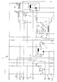
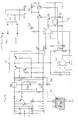
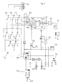
- the basic structure of the transistor measuring device shown in the drawing consists of a power supply unit 1, a start / stop device 2, a conversion module 3, a module "A" 4, a relay card 5, an NF / HF switchover and display logic 6, a switching time measuring device 7, a display for occupancy of the transistor connections 8, a display for doping sequence: NPN / PNP 9, clock simulator with display 10 and the + U BE / -U EB -mV voltmeter 11.
- the oscillator 12 is followed by a delay flip-flop 13 for realizing a duty cycle of 1: 1, as a result of which the binary counter 29 is always driven with a symmetrical signal.
- a reset button 14 is provided on the delay flip-flop 15, via which all the memory modules connected to it are set in an orderly starting situation.
- the preferred circuit is also provided with an RC combination 16, the node of which is inextricably linked to the set / reset contact of the reset button 14.
- a potentiometer 20 is provided in the oscillator circuit 12, so that the oscillator frequency f OSZ before an LF transistor check . is freely adjustable within a given range.
- the switch 28 from the relay 53 for changing the oscillator frequency is located in the oscillator 12, as a result of which it is possible to switch from a low-frequency transistor test to a high-frequency transistor test, so that the transistor measuring device can be used for both NF transistors and HF Transistors can be examined.
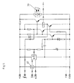
- a further preferred embodiment of the invention is characterized in that the comparator 40 is followed by a silicon germanium detector, the one Opto-coupler 39 and an impedance converter 99, the impedance converter having a dual voltage supply and a low-resistance output and the output on the one hand with a low-resistance via a germanium transistor 100 and a silicon diode 101 connected to its emitter at the reference voltage and on the other hand on displays for "Silicon" 102 or "Germanium” 103 is present.
- the transistor measuring device can also determine automatically and without external intervention from which semiconductor output doping material the transistor to be examined is made.
- the output voltage of a fixed voltage regulator -IC 104 is possible by raising the reference potential with the addition of a Zener diode 105 by means of a potentiometer 106 at the desired level.
- this output voltage is fed to the plus input of a fully electronic relay 107, which only switches the regulated plus voltage through to its output when the control input "S" 108 from the fully electronic relay 107 through the activated optocoupler 39 via the collector-emitter path of the optocoupler to reference potential lies. Only then is the dual voltage divider 109, the impedance converter 99 and the silicon germanium light indicators 102 or 103 connected to the operating voltage required for their operation, for which reasons the light indicators 102 or 103 only appear from the active side after a transistor check has been completed.
- the relatively high-resistance + U BE voltage in the case of NPN transistors and the likewise relatively high-resistance -U EB voltage in the case of PNP transistors are always supplied with the correct polarity to the very high-resistance input of the operational amplifier 99 connected as an impedance converter via a relay circuit 110 , whereby the base / emitter voltages are always available with the desired polarity and undistorted and low-resistance at the output of the impedance converter 99.
- a further advantageous embodiment is given with the low-impedance output resistance of the impedance converter 99 in that even very low-impedance analog measuring mechanisms for voltage indication can be switched between it and the virtual zero point 111 of the circuit with only one directional deflection.
- a digital mV meter 11 is connected between the said measuring points, which means that characteristic voltage fluctuations under the same transistor types from the outset, e.g. can be selected for measurement purposes.
- the output voltage of the impedance converter controls the transistors 112, 113 connected as fully electronic relays, at the output of which the illuminated indicators for "silicon” 102 and “germanium” 103 are connected.
- an optocoupler 39 is provided for direct control of the fully electronic relay 107, which enables signal transmission between the electrically insulated circuits with different voltage levels, whereby on the one hand no electrical and on the other hand a contactless connection between two circuits with different voltage potentials was created.
- Another preferred embodiment of the invention is characterized in that the carry output signal "CY" coming from the binary counter 29 is used for the entire control of the LF / HF switching and display logic.
- the carry output signal "CY” clocks the four delay flip-flops 48 on a clock line 47 at the same time via an input socket 45 and an exor gate 46, which means that the information present at the respective data inputs is on the one hand for the optical displays "Low frequency transistor check” 49, "High frequency transistor check” 50, “Transistor defective” 51, "Measurement completed” 52 and on the other hand to control a relay 53 for NF / HF switching to the respective Q outputs of the delay flip-flops 48 themselves.
- the entire circuit is aligned via the input socket 54, with which the entire logic is prepared for a "full measurement”, which is indicated by the optical light display “full measurement” 55.
- the HF transistor check is continued without any external addition, since an AND gate 58 with an OR gate 57 at the output of the overall logic, the output signal produced by a retriggerable monoflop 59 at the output of the logic, not at the output 60 of the circuit appears, whereby the oscillator 12 is not stopped.
- the light indicator 50 "RF transistor check" goes out only after the last RF transistor check has been completed.
- the then appearing carry signal "CY” simultaneously activates the light indicator 51 "transistor defective” and the drop of the previously drawn relay 53, as well as on the one hand the timing of a delay flip-flop 61, which causes the light indicator 52 "measurement completed” to light up and from its Q output, a log.0 signal for locking the start / stop device is emitted via an OR gate 57 located at the output of the logic, and on the other hand the timing of a delay flip-flop located in the start / stop device 15, which stops the oscillator.
- the remaining possibility of influencing the circuit is possible during a test operation of an LF or HF transistor if the stop signal is sent from the evaluation logic via an OR gate 62 to the clock input of the subsequent delay flip-flop 61, whereupon the indicator light 52 "measurement completed "and the log.0 signal appearing at its Q output for one Locking via a gate circuit 22 in the start / stop device ensures that the oscillator frequency ° can have no influence on the binary counter 29. Furthermore, the stop signal passes through the input of a subsequent OR circuit 57 to the output 60 of the circuit, as a result of which the oscillator 12 in the start / stop device is stopped immediately.
- a "full measurement” can be carried out with the circuit, with which an NF transistor check is carried out first and which changes seamlessly after the first test interval to the RF transistor check, without having to influence the circuit for this purpose. It shows the type of transistor test, LF / HF transistor test via optical displays 49, 50 and also indicates via light indicators 51, 52 whether the device under test is defective and when the measurements have been completed.
- a special position is the measurement type described above and the associated optical display 55 for a full measurement, because the preferred circuit allows the external influence on the program flow, which in addition to the full measurement also individual measurements and the combination of "step checks" in the measurement type full measurement and Individual measurements are feasible.
- the CY simulator 63 the RS flip-flop 64 connected to it, an RDR combination 65 connected to the Q output of the RS flip-flop 64 mentioned, and the Digit key 66 is provided for choosing an RF transistor check.
- the button 66 “RF transistor check” is actuated once and the retriggerable monoflop 68 is triggered via the RS flip-flop 64 and the delay flip-flop connected to it, at whose output the simulated CY signal is triggered the intended closed exor gate 46 influences the delay flip-flops 48 connected to the clock line 47, switching from the NF to the RF transistor check.
- the button 70 in the preferred circuit is "NF transistor check", the RS flip-flop 71 connected to it, the delay flip-flop 69, which is used for the "full measurement” indicator light. is responsible and the AND gate 58 connected to the Q output of said delay flip-flop 69 is provided.
- the button 70 "LF transistor check” is operated once, after which a bounce-free pulse from the RS flip-flop 71, the delay flip-flop 69 clocks.
- the optical light display 55 "full measurement” goes out and there is a log at the AND gate input 58. 1 level on.
- the CY signal emitted by the binary counter 29 via the exor gate 46 to the common clock input 47 of the four delay flip-flops 48 appears at the output of the circuit for signal conversion 73 or. at the output of the retriggerable monoflop 59, a simulated stop signal which passes unhindered via the AND gate 58 and the OR gate 57 to the start / stop device, which indirectly stops the oscillator 12.
- the measuring electronics are set up for a subsequent RF transistor check, this can only be initiated by pressing the start-stop button 27 again, which is indicated by the constantly illuminated oscillator display 19.
- An exclusive-OR gate 46 is provided in the input circuit, which on the one hand allows the signal coming from the binary counter 29 as well as the signal coming from the CY simulator 63 to be fed to the clock line 47 and on the other hand assumes a converter function, which means that the signals with two different looks Delay flip-flops 48 connected to the output of the exor gate can be clocked.
- a CY simulator 63 is provided which, in conjunction with the exclusive-OR gate 46 connected to the output line, allows the simulation of the CY signal coming from the binary counter 29, thus using the key 66 "RF transistor located at the input of the circuit -Check "influence on the preprogrammed program flow can be exerted.
- the circuit works in such a way that after actuation of the input key 66 "RF transistor check” the RS flip-flop 64 passes a bounce-free pulse on the output side to the clock input of the delay flip-flop 67, whereby the Q output logs. Assumes 1 level and the retriggerable monoflop 68 triggers, which on the one hand exor gate 64 with a log.
- an inverter 72 connected to the monoflop output rotates the signal by 180 °, whereby the delay flip-flop 67 is automatically reset and the circuit of the CY simulator 63 is in the initial situation.
- the simulated monoflop signal can thus actually only be effective for the calculated time or the monoflop time.
- the preferred circuit includes a circuit unit 73 for signal conversion, which is structurally identical to the CY simulator 63.
- the associated delay flip-flop 48-1 is clocked by the CY signal, whereupon the associated retriggerable monoflop 59 is triggered by the Q output of the delay flip-flop 48-1, which on the one hand has its output signal is passed via an AND gate 58 and an OR gate 57 to the output 60, as a result of which the start / stop oscillator 12 is stopped in the start / stop device and, on the other hand, its output signal is passed to the downstream inverter input 74, thus the delay flip-flop 48-1 is automatically reset in the initial situation.
- a signal conversion from log.1 to log.0 to log.1 takes place as a single log. 1 signal for the start / stop oscillator 12 in the start-stop device instead.
- a display and switching logic which, on the one hand, shows which type of transistor test is in progress, LF or HF transistor check 49, 50 and further provides information as to whether a transistor is defective 51 and when a measurement is completed 52 and on the other hand switches with the optical display change from LF transistor check to HF transistor check or vice versa a relay 53 for pulling in or out, with which circuit-related changes in the transistor test circuit by measuring resistance change 36- and in start / Stop oscillator circuit 12 a change in the fundamental frequency takes place.
- This is done in such a way that the delay flip-flops on a clock line are clocked simultaneously from the CY signal from the binary counter 29, with each CY signal the binary information present at the data inputs relating to the Q outputs of the delay lines.
- Flip-flops 48 are switched through and, on the one hand, activate the optical light indicators according to the switched-through information and, on the other hand, the relay 53 for LF / HF switchover is activated or released.
- a "locking delay flip-flop” 61 is provided, which automatically locks the start / stop device with each completion of a measurement, and particularly important when using the simulator as a clock generator, so that unwanted clock signals are given after completion of a measurement , have no influence on the binary counter 29. This is done in such a way that an OR gate 62 is provided with two inputs, on the one hand the stop signal of the evaluation logic and on the other hand the signal from the Q output of the delay flip-flop 48-2, that "transistor defective" 51 is responsible for the optical light display.
- the output of the OR gate 62 is switched, as a result of which the locking delay flip-flop 61 is clocked and the log appearing at its Q output. 0 signal locks the start / stop device.
- the time of locking can be recognized optically by the brightening light indicator "measurement completed".
- the preferred circuit provides a device which allows intervention in the program sequence in such a way that, in contrast to the "full measurement" which provides for an LF and HF transistor test, only an LF transistor test is carried out .
- This is done in such a way that after actuation of the digit key 70 "LF transistor check" via an RS flip-flop 71 a bounce-free pulse reaches the clock input of a delay flip-flop 69 connected thereafter, which on the one hand causes the "full measurement” indicator light 55 goes out and, on the other hand, an AND gate input 58 connected to the Q output of the delay flip-flop 69 with a log. 1 level is applied.
- a log appearing at the output of the signal converter circuit 73 after an LF transistor check. 1 signal passes through the downstream AND gate 58 and OR gate 57 to the start / stop device, as a result of which the oscillator 12 is stopped and the LF transistor check is completed.
- a further advantageous embodiment of the invention is characterized in that bounce-free pulses are sent from a simulator to an input terminal "S" 23 of the start / stop device provided for this purpose, so that in addition to the measurement types full measurement and individual measurements, step checks in the measurement types Full measurement and single measurements are feasible.
- the measures already described for influencing the execution of the program apply, but the execution speed is no longer specified by the oscillator 12 of the start / stop device, but this can be done step by step in an arbitrarily expanded form step by step via the key 75 "simulator" be determined.
- the oscillator display 19 by the optical display "Simulator” has been replaced, with which the simulator display 76 shows itself from the active side with each voltage analysis around the test object or the inactive simulator display 76 shows the change to the next lower test step.
- the optical display "measurement completed” 52 which also locks the measuring electronics at the same time, so that further actuation of the simulation key has no effect.
- the locking of the start / stop device and the associated zero function of the simulator is also ensured if the stop signal from the evaluation logic influences the LF / HF switchover and display logic during the test process.
- a circuit unit has thus been created, as a result of which there is a third type of measurement which allows a step-by-step check in the measurement types full measurement and individual measurements.
- the oscillator display 19 is replaced by the optical light display "simulator" 76.
- Another preferred embodiment of the invention is characterized in that the electromagnetic component "relay" is replaced by a fully electronic and contactless circuit.
- the implementation takes place in such a way that the second transistor 42 connected to the base of a series transistor 41 is used to control the series transistor 41. Is a log at the base of the second transistor 42. 0 level, its collector-emitter path is high-resistance and the series transistor 41 remains switched through by its resistor connected to the base, so that the collector-emitter path of the series transistor 41 remains low-resistance. Is a log at the base of the second transistor 42. 1 level on, its collector-emitter path is low-resistance, as a result of which the series transistor 41 is blocked.
- a further preferred embodiment of the invention is characterized in that the signals coming from a start / stop oscillator 12 are not only used to control the binary counter 29, but also that these signals are also output via the output socket "t" of the start / stop device to the measuring input socket 77 "t X " of the switching time measuring device.
- a time measurement is carried out with each positive rising clock edge at the measurement input 77 in such a way that, on the one hand, an OR gate (I) 79 connected to it via an OR gate (I) 78 and its output is an input from the AND gate (II) 80 with log.
- Controls 1 level whereby the pulses coming from an X-TAL oscillator 81 can enter a counter via the AND gate (II) 80 and, on the other hand, a retriggerable monoflop via the OR gate (I) 78 and (II) 82 83 is triggered, with its output signal via OR gate (III) 84, the counter is enabled via its reset input 85 for the incoming pulses at its clock input 86. Reached before log level change. 1 on log. 0 at the measurement input 77, a stop signal of the evaluation logic and the clock input from the delay flip-flop 87, on the one hand the Q output from the delay flip-flop 87 goes to log.
- a switching time measuring device has been created, with which e.g. for special application conditions in measuring technology can be selected for switching transistors for data processing systems based on their switching speed under transistors of the same name.
- Each switching time measurement is automatically initiated and brought to an end for all types of measurement without any external addition, the result of the switching time with the completion of a transistor check with the brightening of the optical indicator 52 "measurement complete" being read directly from a seven-segment display 88 resp. there is no display if the transistor is defective.
- an input button 89 is located in the switching time measuring device, via which the measuring circuit can be prepared for external measurements.
- the digit key 89 "t X -external" is pressed once, after which the RS flip-flop 90 gives a bounce-free pulse to the clock input of the delay flip-flop 91, the Q output of which, on the one hand, is the AND gate (III) 92 opens and, on the other hand, a log to the reset input of the counter via OR gate (III) 84. 1 level leads, whereby the counter for incoming pulses is enabled at its clock input 86.
- the readiness for measurement of an external signal via the measurement input socket 93 is indicated by the optical light display 96.
- the signal to be measured is passed through the input socket 93 to the measuring circuit, the measurement being initiated with an O-to-1 signal or with a positive clock edge and with the drop in the signal to be measured from log. 1-on-log. 0 is completed. °
- a clock edge is formed with the falling edge via an inverter 94 via the AND gate (III) 92, which clocks the delay flip-flop 95 and the log applied to its data input. 0 information on the Q output switches, thereby locking the AND gate (I) 79, so that no clock edge at the measurement input 93 can influence the measurement circuit.
- the measured time can be read directly from the seven-segment display and only goes out when the reset button 14 is pressed, which places the circuit in its original state, which can be recognized from the inactive illuminated display 96 "t X -extern".
- the specially developed circuit for measuring the transistor switching times can a.) As a separate measuring device with the features described above and b.) Also without the counter circuit with the associated seven-segment display 88 (Fig. 12 ) as a separate “measuring circuit" to expand the measuring range for frequency counters etc. etc. and be sold.
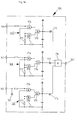
- Another advantageous embodiment of the invention is characterized in that the electromechanical relay Fig. 5 / Fig. 10 (110) can be replaced by a light-controlled AC / DC switch Figure 13, which on the one hand enables a direct and fast voltage display to be implemented, since the switching of the analog voltages to be measured is instantaneous and, on the other hand, there are, besides other advantages, much cheaper wiring .
- four differential amplifiers (114, 115, 116, 117) constructed as voltage followers are provided, each non-inverting amplifier input via the collector-emitter path of a photo transistor (118, 119, 120, 121) is connected to the reference potential. If there is a log at the common control input "S" (122).
- the transistors (123, 124) are switched on and the photodiodes (125, 126) in their collector circuits cause the light transistors to switch the phototransistors (119, 121) through to the reference potential, which means that only those at inputs E1 and E (1) (127, 128) applied signals to the outputs A1 and A (1) (129, 130) are switched.
- the analog signals present at inputs E2 and E (2) (131, 132) are only switched through to outputs A1 and A (1) (129, 130) if control input "S" (122) a log Sets 0 level.
- the use of the light-controlled switch for the analog and digital range is determined by the external wiring.
- a further preferred embodiment of the invention is provided with the use of a fully electronic and contactless relay (G 93 18 765.3), with which two further advantageous configurations can be realized: a.) The electromechanical relay FIG. 9 (53) for actuating the switches S1 ( Fig. 2) or S2 (Fig. 4) and b.) The electromechanical relays of the relay card Fig. 4 (34), can be replaced by fully electronic and contactless relays. Due to the fixed digital "interlocking" of the search device with the The preferred circuit allows measuring circuits to easily increase the oscillator frequency to, for example, 500 Hz (!), Which limits the checking time of an LF transistor to a maximum of 2 ml-seconds.
- the NF transistor checks can be reduced to a maximum of eight test steps, which theoretically can be used to check more than 60 NT transistors on a circuit board in one second and at the same time more than 450 associated physical data can be obtained.
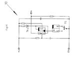
- 15 shows the circuit of the fully electronic and contactless relay symbol
- FIG. 16 shows the associated switching symbol / symbol.
- a positive voltage present at the control input (137) brightens up the luminescence diode (138), which as a coupling element emits the optical signal on the surfaces of the light-sensitive phototransistors (139), whereupon the insulation layers change from the extremely high-resistance to the low-resistance state, which means that the path Terminal A (140) / Terminal K (141) and vice versa via the phototransistor (139) no longer represents a resistor for the current applied.
- the arranged inverter (142) turns the luminescence diode (143) dark, whereupon the insulation layers of the phototransistors (144) show high resistance and do not allow current to flow from terminal B (145) to terminal K (141) and vice versa. However, if there is a reference potential at S (137), the distance terminal A (140) / terminal K (141) and vice versa appears from the high-resistance side.
- the route terminal B (145) / terminal K (141) shows low resistance in both directions, since the luminescent diode (143) is activated via the inverter (142), whereupon the Sweep insulation layers of the phototransistors (144) in the low-resistance area.
- the value of the resistors (146) determines the luminous flux of the diode (138, 143) and thus the insulation resistance of the phototransistors (139, 144). If there is no signal at the control input S (137), the resistor (147) keeps the distance between terminal A (140) / terminal K (141) low-impedance or, with a high-resistance selection, holds the output of the inverter (142) at log.1- Level.
- the NC decoder Fig. 18 (158) consists of three identical logic circuits (165), the inputs (166, 167, 168 ) are directly connected to the measuring input socket (157) via the relay-controlled switches (169, 170, 171) and their outputs (172, 173, 174) are connected to the AND gate (175). If there is correct contact between the transistor and the measuring input socket (157) and the device under test is not defective, the rectangular signal coming from the NAND is present at all three inputs (166, 167, 168) via the AND gate (155) Gate (176) is transformed by the resistors (177, 178) in such a way that a log.1 level is set at the NAND gate output (179). This Log.1 information passes through the outputs (172, 173, 174) to the AND gate (175), which appears at the output of the NC decoder (158), the output socket (160), a 0-to-1 signal leaves.
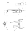
- a further preferred embodiment of the invention is provided with the SMD component test pin, which allows the direct checking of active SMD semiconductor components on the printed circuit boards using only a three-wire measuring cable.
- the measuring cable (180) is connected on the one hand to the measuring input socket (157) and on the other hand via a jack coupling (181) to the jack plug (182) of the probe holder (183).
- the probe (186) is firmly screwed to the probe carrier (183) by the thread (184, 185), where ° the probe (186) itself carries the three test probes (187).
- the three-wire measuring cable (180) is connected securely to the test probes (187) by soldering the ends of the strands to the cup (188) of the test probes (187).
- the SMD component test pin can easily be carried in the breast pocket of the shirt, since a bracket (189) is provided.
- the transistor measuring device works as follows:
- the start / stop device 2 (FIG. 2) has an RC combination 16 which, when the transistor measuring device is started up, puts all of the delay flip-flops connected to it in an orderly starting situation, so that the reset button 14 does not move with the first , but only has to be actuated once before the subsequent transistor checks in order to put the memory modules in a correct measurement output situation.
- the start-stop device 2 also includes a start button 27, with which the delay flip-flop 15 is set and with the log appearing at its Q output. 1 signal the start / stop oscillator 12 is started.
- a delay flip-flop 13 is connected downstream of the oscillator 12, so that the signal at the Q output from the delay flip-flop 13 has a pulse duty factor of 1: 1.
- the fact that the oscillator 12 initiates its vibrations with a positive clock edge and that the pulse duty factor is 1: 1 and also that the 1st measurement time is the same as the subsequent measurement times is indicated by the oscillator display 19.
- the symmetrical output signal is passed through one of four available inputs OR gate 21 via one of two existing inputs of an AND gate 22 on the one hand to the output socket 24, from where it is forwarded to the switching time measuring device 7 and on the other hand via an output terminal to the clock input of a four-bit binary counter 29 (FIG. 3) .
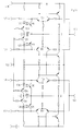
- the 3-bit binary code appearing at the outputs Q1, Q2 and Q3 of the binary counter 29 is converted into a decimal in a binary / decimal converter which is made up of the AND gates 30 and the inverters 31 with downstream driver stages 32 -Code converted, of which the signals 1, 2, 3, 4, 5 and 6 are present on the display 8 (FIG. 1) for the assignment of the transistor connections and also via the output terminals a, b which are used in parallel with the outputs 1 to 5 , c, d and e to the relay card 5 (Fig. 4) are performed.
- the Q4 output of the binary counter 29 is passed on the one hand via a driver stage 32 to the output N / P to an NPN / PNP display 9 (FIG.
- the Q1, Q2 and Q3 signals of the binary counter 29 are routed to a circuit consisting of Exor gate 33, the signals appearing at the output terminals X, Y and Z being triggered on the one hand by the signals from the AND gate outputs 30 the exor gate inputs 33 signals, as well as on the other hand, are shaped by the signals passed from the Q4 output of the binary counter 29 to the exor gate inputs 33 in such a way that at an NPN transistor check, terminal X is always present a log 0 level and a log at terminals Y and Z.
- the comparator 40 responds when a certain voltage drop occurs at the collector of the transistor under investigation, the formation of which solely affects the diode circuit consisting of the four silicon diodes between the input terminal Z and the output terminal III on the module "A" 4 (Fig. 4).
- the comparator 40 then switches off the oscillator 12 (FIG. 2), with which the measurement is completed, which is indicated by the illuminated display 52 (FIG. 9) “measurement completed”.
- the optical assignment 8 (FIG. 1) shows the pin assignment of the transistor in conjunction with the three numbers 1, 2 and 3 on the measuring input socket or on the test prods of the test terminals. If the transistor is defective, the indicator lights show the inactive side.
- the NPN / PNP display 9 shows the doping sequence of the test object via two light-emitting diodes 97, 98 (FIG. 6). If the transistor is defective, the NPN / PNP display 9 indicates the resetting of the entire logic with the NPN display 97, while the remaining information such as “measurement completed” or “transistor defective” until a new measurement is initiated by actuating the reset Key 14 (FIG. 2) remain stored.
- the transistor measuring device shown it is also determined at the same time whether it is a germanium transistor or a silicon transistor.
- the associated silicon germanium detector is shown in FIG. 10.
- the detector includes the optocoupler 39 which, via the control input "S" 108, switches the stabilized voltage generated via the components voltage regulator IC 104, Zener diode 105 and the adjustable resistor / potentiometer 106 to the output terminal U A of the electronic relay 107, as a result of which active dual voltage divider 109 can provide the dual voltage supply required for the operation of the impedance converter 99.
- the base / emitter voltage of interest can thus be fed from the relatively high-resistance transistor test circuit from terminals I and III (FIG.
- the base-emitter voltages that are important to be detected for measuring circuits, but are strongly scattered, are compared with those in the output circuit of the impedance converter circuit 99 switched digital millivolt meters 11 can be read precisely, which enables correct selection. If the transistor is defective, there is no display.
- each switching time measurement is initiated with the positive rising clock edge, which is led from the output socket 24 (FIG. 2) of the start / stop device 2 to the measurement input 77.
- the measurement initiation signal arrives at the AND gate 80, which opens and allows the pulses coming from the oscillator 81 to enter the counter.
- the simultaneously triggered monoflop 83 stops with its log. 1 signal clears the counter. If no stop signal from the socket 60 (FIG. 9) of the LF / HF switchover and display logic 6 reaches the clock input from the delay flip-flop 87, the level of the measurement initiation signal changes to log.
- the transistor turn-on time becomes directly from the seven-segment display 88 when a transistor check is completed reproduced. If the transistor to be tested is defective, there is no display.
- button 89 is pressed after pressing reset button 14 (FIG. 2).
- t X -external operted once, the indicator 96 indicating the readiness of a Measurement.
- the signal to be measured is entered via the measurement input 93. The descriptions described above apply to the measurement process.
Landscapes
- Physics & Mathematics (AREA)
- General Physics & Mathematics (AREA)
- Testing Of Individual Semiconductor Devices (AREA)
Applications Claiming Priority (4)
| Application Number | Priority Date | Filing Date | Title |
|---|---|---|---|
| DE9307408U DE9307408U1 (de) | 1993-05-15 | 1993-05-15 | Transistorprüfgerät |
| DE9307408U | 1993-05-15 | ||
| DE9318765U | 1993-12-08 | ||
| DE9318765U DE9318765U1 (de) | 1993-12-08 | 1993-12-08 | Vollelektronische- und kontaktlose Relais |
Publications (1)
| Publication Number | Publication Date |
|---|---|
| EP0626585A1 true EP0626585A1 (fr) | 1994-11-30 |
Family
ID=25960862
Family Applications (1)
| Application Number | Title | Priority Date | Filing Date |
|---|---|---|---|
| EP94107278A Withdrawn EP0626585A1 (fr) | 1993-05-15 | 1994-05-10 | Appareil de mesure de transistor programmable et totalement électronique |
Country Status (1)
| Country | Link |
|---|---|
| EP (1) | EP0626585A1 (fr) |
Cited By (3)
| Publication number | Priority date | Publication date | Assignee | Title |
|---|---|---|---|---|
| CN106383312A (zh) * | 2016-12-01 | 2017-02-08 | 北京简佑科技有限公司 | 一种电机状态检测电路及电机状态显示装置 |
| CN108107301A (zh) * | 2018-02-28 | 2018-06-01 | 广西玉柴机器股份有限公司 | 光耦测试装置 |
| CN115425961A (zh) * | 2022-11-04 | 2022-12-02 | 西安水木芯邦半导体设计有限公司 | 一种高压模拟开关阵列电路 |
Citations (4)
| Publication number | Priority date | Publication date | Assignee | Title |
|---|---|---|---|---|
| US3478264A (en) * | 1968-01-31 | 1969-11-11 | Ram Tool Corp | Scr,diode and transistor analyzer |
| US3601698A (en) * | 1969-01-21 | 1971-08-24 | Milton E Thurman Jr | Semiconductor tester having visual display |
| DE2059463A1 (de) * | 1970-12-03 | 1972-06-08 | Paul Majerhofer | Suchlaufautomatik fuer Transistorpruefung |
| EP0048324A1 (fr) * | 1980-09-24 | 1982-03-31 | Walter Hanselmann AG Fesy Elektronik | Appareil pour tester des composants semi-conducteurs actifs |
-
1994
- 1994-05-10 EP EP94107278A patent/EP0626585A1/fr not_active Withdrawn
Patent Citations (4)
| Publication number | Priority date | Publication date | Assignee | Title |
|---|---|---|---|---|
| US3478264A (en) * | 1968-01-31 | 1969-11-11 | Ram Tool Corp | Scr,diode and transistor analyzer |
| US3601698A (en) * | 1969-01-21 | 1971-08-24 | Milton E Thurman Jr | Semiconductor tester having visual display |
| DE2059463A1 (de) * | 1970-12-03 | 1972-06-08 | Paul Majerhofer | Suchlaufautomatik fuer Transistorpruefung |
| EP0048324A1 (fr) * | 1980-09-24 | 1982-03-31 | Walter Hanselmann AG Fesy Elektronik | Appareil pour tester des composants semi-conducteurs actifs |
Non-Patent Citations (3)
| Title |
|---|
| "pc-controlled semiconductor tester pc-tt90", ELEKTOR ELECTRONICS, vol. 17, no. 188, April 1991 (1991-04-01), LONDON,GB, pages 44-50, XP000230069 * |
| "tup tun tester", ELEKTOR BOOK 75, 1977, CANTERBURY,GB, pages 20-26 * |
| "Zeigt her eure Beinchen", FUNKSCHAU, no. 17, August 1983 (1983-08-01), MüNCHEN,DE, pages 83-84 * |
Cited By (6)
| Publication number | Priority date | Publication date | Assignee | Title |
|---|---|---|---|---|
| CN106383312A (zh) * | 2016-12-01 | 2017-02-08 | 北京简佑科技有限公司 | 一种电机状态检测电路及电机状态显示装置 |
| CN106383312B (zh) * | 2016-12-01 | 2023-06-27 | 北京简佑科技有限公司 | 一种电机状态检测电路及电机状态显示装置 |
| CN108107301A (zh) * | 2018-02-28 | 2018-06-01 | 广西玉柴机器股份有限公司 | 光耦测试装置 |
| CN108107301B (zh) * | 2018-02-28 | 2023-09-19 | 广西玉柴机器股份有限公司 | 光耦测试装置 |
| CN115425961A (zh) * | 2022-11-04 | 2022-12-02 | 西安水木芯邦半导体设计有限公司 | 一种高压模拟开关阵列电路 |
| CN115425961B (zh) * | 2022-11-04 | 2023-03-10 | 西安水木芯邦半导体设计有限公司 | 一种高压模拟开关阵列电路 |
Similar Documents
| Publication | Publication Date | Title |
|---|---|---|
| DE3111852C2 (fr) | ||
| DE3877862T2 (de) | Bestimmung der ausrichtung von bauteilen. | |
| EP2211147B1 (fr) | Procédé de contrôle du fonctionnement d'une circuit électrique | |
| EP0507168A1 (fr) | Méthode pour tester des circuits integrés semi-conducteurs soudés sur platines, et utilisation d'un testeur de transistor pour cette méthode | |
| DE2703880C3 (de) | Elektrisches Prüfgerät mit akustischer, quantitativer Analoganzeige für Widerstand und Spannung | |
| DE69325751T2 (de) | Verfahren zum Testen des Kontakts zwischen einem integrierten Baustein und einer Leiterplatte | |
| DE69021036T2 (de) | Test-Anordnungssystem für integrierte Schaltungen unter Verwendung von lateralen Transistoren. | |
| EP0626585A1 (fr) | Appareil de mesure de transistor programmable et totalement électronique | |
| DE19632457C1 (de) | Schaltungsanordnung zur Überwachung eines Sensors | |
| DE19906932B4 (de) | Binäreingabegerät | |
| DE3505531C2 (fr) | ||
| WO2004086069A1 (fr) | Procede d'essai de composants d'une plaquette de circuit imprime | |
| DE3022279C2 (fr) | ||
| DE69709329T2 (de) | Modul mit schnittstelle zur prüfung und diagnose einer elektronischen telekommunikationseinrichtung | |
| DE2903383C2 (de) | Separates Testgerät für adressierbare Schaltungen | |
| EP0544148B1 (fr) | Méthode de programmation pour circuits intégrés | |
| EP0919821A1 (fr) | Dispositif de détection et méthode de fonctionnement correspondante | |
| DE69707108T2 (de) | Sonde für fehleraktivierungsvorrichtungen | |
| DE10151053B4 (de) | Schaltungsanordnung | |
| EP3899558A1 (fr) | Procédé et dispositif de contrôle | |
| DE102018217406B4 (de) | Verfahren und Vorrichtung zum elektrischen Prüfen einer elektrischen Baugruppe | |
| DE1910750C3 (de) | Elektrische Schaltungsanordnung zum Einstellen einer Vielzahl gleichartiger Meßkanale einer Einrichtung zur zerstörungsfreien Materialprüfung auf gleiche Empfindlichkeit | |
| DE9307408U1 (de) | Transistorprüfgerät | |
| EP0013706A1 (fr) | Dispositif pour la surveillance automatique de l'état de charge de la source d'alimentation indépendante du secteur et de l'humidité dans le répondeur d'un système de localisation de véhicules | |
| DE3150546A1 (de) | "wartungseinrichtung fuer zaehlpunkte" |
Legal Events
| Date | Code | Title | Description |
|---|---|---|---|
| PUAI | Public reference made under article 153(3) epc to a published international application that has entered the european phase |
Free format text: ORIGINAL CODE: 0009012 |
|
| 17P | Request for examination filed |
Effective date: 19940510 |
|
| AK | Designated contracting states |
Kind code of ref document: A1 Designated state(s): AT BE CH DE DK ES FR GB GR IE IT LI LU MC NL PT SE |
|
| RAX | Requested extension states of the european patent have changed |
Free format text: SI |
|
| 17Q | First examination report despatched |
Effective date: 19980123 |
|
| STAA | Information on the status of an ep patent application or granted ep patent |
Free format text: STATUS: THE APPLICATION IS DEEMED TO BE WITHDRAWN |
|
| 18D | Application deemed to be withdrawn |
Effective date: 19991007 |