EP0626659A1 - Appareil, système et méthode appliqués au traitement distribué - Google Patents
Appareil, système et méthode appliqués au traitement distribué Download PDFInfo
- Publication number
- EP0626659A1 EP0626659A1 EP94303756A EP94303756A EP0626659A1 EP 0626659 A1 EP0626659 A1 EP 0626659A1 EP 94303756 A EP94303756 A EP 94303756A EP 94303756 A EP94303756 A EP 94303756A EP 0626659 A1 EP0626659 A1 EP 0626659A1
- Authority
- EP
- European Patent Office
- Prior art keywords
- memory
- data
- arguments
- circuitry
- active
- Prior art date
- Legal status (The legal status is an assumption and is not a legal conclusion. Google has not performed a legal analysis and makes no representation as to the accuracy of the status listed.)
- Withdrawn
Links
Images
Classifications
-
- G—PHYSICS
- G06—COMPUTING OR CALCULATING; COUNTING
- G06F—ELECTRIC DIGITAL DATA PROCESSING
- G06F9/00—Arrangements for program control, e.g. control units
- G06F9/06—Arrangements for program control, e.g. control units using stored programs, i.e. using an internal store of processing equipment to receive or retain programs
- G06F9/30—Arrangements for executing machine instructions, e.g. instruction decode
- G06F9/38—Concurrent instruction execution, e.g. pipeline or look ahead
- G06F9/3877—Concurrent instruction execution, e.g. pipeline or look ahead using a secondary processor, e.g. coprocessor
- G06F9/3879—Concurrent instruction execution, e.g. pipeline or look ahead using a secondary processor, e.g. coprocessor for non-native instruction execution, e.g. executing a command; for Java instruction set
-
- G—PHYSICS
- G06—COMPUTING OR CALCULATING; COUNTING
- G06F—ELECTRIC DIGITAL DATA PROCESSING
- G06F15/00—Digital computers in general; Data processing equipment in general
- G06F15/76—Architectures of general purpose stored program computers
- G06F15/78—Architectures of general purpose stored program computers comprising a single central processing unit
- G06F15/7807—System on chip, i.e. computer system on a single chip; System in package, i.e. computer system on one or more chips in a single package
- G06F15/7821—Tightly coupled to memory, e.g. computational memory, smart memory, processor in memory
Definitions
- the present invention relates in general to data processing and in particular to apparatus, systems and methods for distributed processing.
- the CPU becomes burdened not only with the task of performing all arithmetic operations but also with the task of controlling the transfer of data to and from memory.
- the memory in turn must be large enough to handle the initial raw data and all the intermediate results.
- the traffic on the address and data buses substantially increases as data and results are exchanged between the memory and the CPU.
- an active memory device which includes a data memory including rows and columns of storage locations for holding raw data and computational results.
- a broadcast memory is further provided which includes rows and columns of storage locations for holding control instructions and computational arguments.
- a data path is provided which is operable to supply selected computational arguments received from the broadcast memory to selected words of raw data received from the data memory and provide computational results in response.
- Control circuitry is additionally provided which is operable in response to control instructions received from the broadcast memory to control the transfer of selected words of raw data and the results between the data memory and the data path, the transfer of the selected arguments from the broadcast memory to the data path, and the application of the selected arguments to the selected words of raw data by the data path.
- Active memory devices embodying concepts of the present invention as well as systems and methods using such active devices, provide significant advantages. Such devices, systems and methods can be used to ease task burdens by performing data processing operations independent of the corresponding central processing unit. Apparatus, systems and methods embodying the present invention allow efficient use of system data and address busses by reducing the data and address traffic between the central processing unit and memory.
- FIGS 1-2 of the drawings like numerals being used for like and corresponding parts of the various drawings.
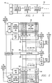
- FIGURE 1 depicts a processing system 10 employing an architecture embodying concepts of the present invention.
- Processing system 10 includes a central processing unit (CPU) 12 coupled to a number of active memory devices 14 by a data bus 16 and an address bus 18.
- CPU 12 which may be for example a general purpose microprocessor, a microcontroller, a digital signal processor, or a graphics processor.
- active memory devices 14 provide for the distributed computing and data handling required for problem solving operations, as discussed in detail below.
- each active memory 14 in system 10 has a pin configuration compatible with the pin configuration of a chosen conventional ("inactive") memory unit (for example a 28-pin pinout). In this fashion, active memories 14 and conventional inactive memories can be interchanged on a given board or other supporting structure.
- active memory devices 14 In addition to minimizing the computation burdens imposed on CPU 12, distributed processing using active memory devices 14 allows for more efficient utilization of data bus 16 and address bus 18. In essence, active devices 14 compress or reduce data such that the exchange of raw data and intermediate results on data bus 16 and the corresponding transmission of addresses on address bus 18 are substantially reduced.
- FIGURE 2 is a functional block diagram of an illustrative active memory 14 embodying the concepts of the present invention.
- Active memory 14 may be constructed as a single chip or module (a "device") which includes a data random access memory 20 (RAM), a broadcast RAM 22, a controller 24 and datapath 26.
- data RAM 20 and broadcast RAM 22 may be fabricated in a standardized configuration for a given set of devices while controller 24 and datapath 26 are customized to meet the operational requirements for a given device or subset of devices.
- Data RAM 20 may be either a static random access memory (SRAM) or a dynamic random access memory array (DRAM).
- SRAM static random access memory
- DRAM dynamic random access memory array
- FIGURE 2 RAM 20 is depicted as a 2k x 8 memory arranged as 128 rows and 128 columns of RAM cells. It should be noted that in addition to the configuration shown in FIGURE 2, any one of a number of alternate RAM architectures may also be used, as is understood in the art.
- circuitry for reading and writing data to and from selected cells in the array including row address circuitry 28, a row address multiplexer 30, first stage decoding (column address) circuitry 32, column address multiplexer 34 and input/output circuitry 36.
- Multiplexer 30 passes address bits to the row address circuitry 28 from either system address bus 18 or from the controller 24.
- multiplexer 34 passes address bits from either the address bus 18 or from controller 24.
- Multiplexers 30 and 34 along with input/output circuitry 36 allow for the transfer of bits of data into the cells of data RAM either from CPU 12 using data bus 16 and address bus 18 or from datapath 26 using internal bus 38.
- first stage decoder 32 multiplexes each set of four adjacent bitlines to form an internal bus 38 which is 32 bits wide (if for example a 256 column memory architecture was used, then the internal bus would be 64 bits wide).
- I/O circuitry 36 includes a four to one multiplexer which selects, in response from address bits from address bus 18, one of four sets of eight adjacent bits on 32-bit internal bus 38 for communication to the system data bus 16. It should be noted that in alternate embodiments the configuration of input/output circuitry may vary depending on such factors as the width of internal bus 38 and the number of lines (bits) communicating with system data bus 16.
- Broadcast RAM 22 may also be either static or dynamic and is similarly associated with circuitry for writing and reading data into and out of its memory cells array including row address circuitry 40, row address multiplexer 42, first stage (column) decoding circuitry 44, multiplexer 46 and input/output circuitry 48.
- broadcast RAM is organized as 2 rows and 128 columns, although alternate row/column organizations may be used in other embodiments.
- the read/write circuitry associated with broadcast RAM 22 operates similar to the read/write circuitry associated with data RAM 20.
- First stage decoder circuitry 44 in the illustrated embodiment performs 4:1 multiplexing on each four adjacent columns of the 128 columns memory cells in broadcast RAM 22 with selected 32 bits coupled to datapath 26 via a second internal bus 50.
- Multiplexers 42 and 46 selectively pass address bits from either system address bus 18 or from controller 24.
- multiplexers 42 and 46 along with input/output circuitry 48 allow for the transfer of data into the cells of broadcast RAM 26 from either CPU 12 via or from controller 24 through datapath 26.
- the specific configurations of row address circuitry 40, multiplexers 42 and 46, first stage decode circuitry 44, and input/output circuitry 48 will vary based on such factors as the numbers of rows and columns in the cell array of broadcast RAM 22, the width of internal bus 50, the number of bits being received from the system address bus 18 and the number of bits (lines) communicating with the system data bus 14.
- the coupling of data bus 16 with input/output circuitry 36 associated with data RAM 20 and input/output circuitry 48 associated with broadcast RAM 22 is preferably made through a single set of pins (D ⁇ -D7) to provide compatibility with conventional memory pinouts.
- the coupling of the read/write circuitry associated with both data RAM 20 and broadcast RAM 22 may be made through a single set of pins (also not shown). Since active memories 14 are part of the system memory, it is preferable that memories 14 take on the characteristics of memory chips. In other words, Memories 14 should be efficient like memory chips, small in size and relying on a minimum number of data and address pins which are compatible with the pin configurations of conventional ("inactive") memory chips.
- Datapath 26 under the control of controller 24 routes data on internal bus 38 and 50 and provides the desired distributed computational capabilities.
- Datapath 26 may be implemented in random logic, in programmable gate array circuitry, or in programmable logic array circuitry, as required to customize the chip or unit to perform the desired computational functions.
- datapath 26 may include adders and multipliers to implement the matrix multiplier example or comparitor circuitry in speech applications.
- controller 24 and datapath 26 may together be implemented in digital signal processing circuitry, such as that found in the Texas Instruments TI-320 family of digital signal processors.
- each Broadcast RAM 22 is placed at the highest address space available for the corresponding number of address bits received by active memories 14 from system address bus 18 This allows each broadcast RAM 22 to be written to or read from without a chip select signal. Further, all the broadcast RAMs 22 of the active memories 14 in system 10 can be accessed simultaneously.
- the broadcast Ram 22 for a given memory 14 receives instructions and data from CPU 12 on data bus 16 for use by controller 26 in carrying out a selected computation.
- CPU 12 writes data into the data Ram 20 of each active memory 14 from data bus 16.
- each data RAM 20 holds a different subset of an overall set of data being operated on.
- each data RAM 20 might hold the data for a corresponding row in the matrices involved.
- a control sequence to be followed by each controller 24 is presented on data bus 16 while the high address bits are presented on address bus 18 such that the control sequence is written into each broadcast RAM 22.
- at least one argument (vector) of the desired computation being performed by system 10 is written into each broadcast RAM 22.
- the same vector is written into all the broadcast RAMs 22 in system 10.
- a dummy location in the broadcast memory space initiates execution of the arguments by the controller 24 and datapath 26 of each active memory device 14.
- controller 24 causes datapath 26 to apply the arguments retrieved from the broadcast RAM 22 to each row of data from data RAM 20, as dictated by the control sequence.
- the results from applying the arguments to a given row of data in the respective data RAM 20 are written by controller 24 through datapath 26 back into one or two selected byte locations along the same row.
- Controller 24 cycles through all row addresses and through the all addresses to the 4 to 1 multiplexer of data RAM first stage decoder 32 such that all the data in the data RAM 20 has been operated on.
- CPU 12 While the active memory devices are operating on the data previously written into each of the data RAMs 20, CPU 12 is freed to attend to other tasks. CPU 12 subsequently returns to retrieve the reduced (compressed) results from the data RAM 20 of each active memory 14 after the active memories indicate completion of the distributed computational tasks.
Landscapes
- Engineering & Computer Science (AREA)
- Theoretical Computer Science (AREA)
- Software Systems (AREA)
- General Engineering & Computer Science (AREA)
- Computer Hardware Design (AREA)
- Physics & Mathematics (AREA)
- General Physics & Mathematics (AREA)
- Computing Systems (AREA)
- Microelectronics & Electronic Packaging (AREA)
- Memory System (AREA)
- Dram (AREA)
Applications Claiming Priority (2)
| Application Number | Priority Date | Filing Date | Title |
|---|---|---|---|
| US6890993A | 1993-05-28 | 1993-05-28 | |
| US68909 | 1993-05-28 |
Publications (1)
| Publication Number | Publication Date |
|---|---|
| EP0626659A1 true EP0626659A1 (fr) | 1994-11-30 |
Family
ID=22085491
Family Applications (1)
| Application Number | Title | Priority Date | Filing Date |
|---|---|---|---|
| EP94303756A Withdrawn EP0626659A1 (fr) | 1993-05-28 | 1994-05-25 | Appareil, système et méthode appliqués au traitement distribué |
Country Status (3)
| Country | Link |
|---|---|
| EP (1) | EP0626659A1 (fr) |
| JP (1) | JPH07152680A (fr) |
| TW (1) | TW363152B (fr) |
Citations (4)
| Publication number | Priority date | Publication date | Assignee | Title |
|---|---|---|---|---|
| EP0354265A1 (fr) * | 1988-08-11 | 1990-02-14 | Siemens Aktiengesellschaft | Circuit intégré à semi-conducteurs ayant un champ de mémoire |
| EP0446721A2 (fr) * | 1990-03-16 | 1991-09-18 | Texas Instruments Incorporated | Mémoire de traitement distribuée |
| EP0513851A2 (fr) * | 1984-10-05 | 1992-11-19 | Hitachi, Ltd. | Unité de mémoire ayant des fonctions arithmétiques et logiques, notamment pour traitement graphique |
| EP0606653A1 (fr) * | 1993-01-04 | 1994-07-20 | Texas Instruments Incorporated | Mémoire de procession distributrice programmable sur le champ |
-
1994
- 1994-05-25 EP EP94303756A patent/EP0626659A1/fr not_active Withdrawn
- 1994-05-30 JP JP15141094A patent/JPH07152680A/ja active Pending
- 1994-12-16 TW TW083112017A patent/TW363152B/zh active
Patent Citations (4)
| Publication number | Priority date | Publication date | Assignee | Title |
|---|---|---|---|---|
| EP0513851A2 (fr) * | 1984-10-05 | 1992-11-19 | Hitachi, Ltd. | Unité de mémoire ayant des fonctions arithmétiques et logiques, notamment pour traitement graphique |
| EP0354265A1 (fr) * | 1988-08-11 | 1990-02-14 | Siemens Aktiengesellschaft | Circuit intégré à semi-conducteurs ayant un champ de mémoire |
| EP0446721A2 (fr) * | 1990-03-16 | 1991-09-18 | Texas Instruments Incorporated | Mémoire de traitement distribuée |
| EP0606653A1 (fr) * | 1993-01-04 | 1994-07-20 | Texas Instruments Incorporated | Mémoire de procession distributrice programmable sur le champ |
Non-Patent Citations (3)
| Title |
|---|
| B. PAWATE ET AL: "Memory based digital signal processing", ICASSP 90, vol. 2, 3 April 1990 (1990-04-03), ALBUQUERQUE, USA, pages 941 - 944 * |
| S. MORTON: "'Intelligent memory chips' give fully programmable synaptic weights", SENSOR FUSION II, 28 March 1989 (1989-03-28), ORLANDO, USA, pages 136 - 150, XP000748374 * |
| T. MARTINEZ: "Smart memory architecture and methods", FUTURE GENERATION COMPUTER SYSTEMS, vol. 6, 1990, pages 145 - 162, XP026648353, DOI: doi:10.1016/0167-739X(90)90030-H * |
Also Published As
| Publication number | Publication date |
|---|---|
| TW363152B (en) | 1999-07-01 |
| JPH07152680A (ja) | 1995-06-16 |
Similar Documents
| Publication | Publication Date | Title |
|---|---|---|
| US5500828A (en) | Apparatus, system and methods for distributed signal processing | |
| US5528550A (en) | Apparatus, systems and methods for implementing memory embedded search arithmetic logic unit | |
| US5546343A (en) | Method and apparatus for a single instruction operating multiple processors on a memory chip | |
| EP3729279B1 (fr) | Organisation de mémoire unifiée pour processeurs de réseau neuronal | |
| US5832290A (en) | Apparatus, systems and method for improving memory bandwidth utilization in vector processing systems | |
| US5475631A (en) | Multiport RAM based multiprocessor | |
| US3787673A (en) | Pipelined high speed arithmetic unit | |
| US5129092A (en) | Linear chain of parallel processors and method of using same | |
| US5537353A (en) | Low pin count-wide memory devices and systems and methods using the same | |
| US8341328B2 (en) | Method and system for local memory addressing in single instruction, multiple data computer system | |
| US5421019A (en) | Parallel data processor | |
| US5832291A (en) | Data processor with dynamic and selectable interconnections between processor array, external memory and I/O ports | |
| EP0446721A2 (fr) | Mémoire de traitement distribuée | |
| US5247613A (en) | Massively parallel processor including transpose arrangement for serially transmitting bits of data words stored in parallel | |
| US20040093465A1 (en) | Cache for instruction set architecture | |
| US20010010057A1 (en) | Semiconductor integrated circuit, computer system, data processor and data processing method | |
| US6804771B1 (en) | Processor with register file accessible by row column to achieve data array transposition | |
| EP0293701A2 (fr) | Système et méthode de traitement en parallèle d'éléments en rapport de voisinage | |
| KR100227133B1 (ko) | 보존된 어드레싱을 이용하는 메모리 장치 및 이를 이용한 시스템및 방법 | |
| KR850004680A (ko) | 집적 프로세서 | |
| JPH06274528A (ja) | ベクトル演算処理装置 | |
| US20080162824A1 (en) | Orthogonal Data Memory | |
| EP0626659A1 (fr) | Appareil, système et méthode appliqués au traitement distribué | |
| JPS63501828A (ja) | マルチゾ−ンプロセツサ | |
| JP3333779B2 (ja) | 行列演算装置 |
Legal Events
| Date | Code | Title | Description |
|---|---|---|---|
| PUAI | Public reference made under article 153(3) epc to a published international application that has entered the european phase |
Free format text: ORIGINAL CODE: 0009012 |
|
| AK | Designated contracting states |
Kind code of ref document: A1 Designated state(s): DE FR GB IT NL |
|
| 17P | Request for examination filed |
Effective date: 19950502 |
|
| 17Q | First examination report despatched |
Effective date: 19980427 |
|
| STAA | Information on the status of an ep patent application or granted ep patent |
Free format text: STATUS: THE APPLICATION IS DEEMED TO BE WITHDRAWN |
|
| 18D | Application deemed to be withdrawn |
Effective date: 19981110 |