EP0626765A1 - Appareil de communication par radio - Google Patents
Appareil de communication par radio Download PDFInfo
- Publication number
- EP0626765A1 EP0626765A1 EP94303630A EP94303630A EP0626765A1 EP 0626765 A1 EP0626765 A1 EP 0626765A1 EP 94303630 A EP94303630 A EP 94303630A EP 94303630 A EP94303630 A EP 94303630A EP 0626765 A1 EP0626765 A1 EP 0626765A1
- Authority
- EP
- European Patent Office
- Prior art keywords
- amplifier
- signal
- output
- radio communication
- supplied
- Prior art date
- Legal status (The legal status is an assumption and is not a legal conclusion. Google has not performed a legal analysis and makes no representation as to the accuracy of the status listed.)
- Granted
Links
Images


Classifications
-
- H—ELECTRICITY
- H03—ELECTRONIC CIRCUITRY
- H03G—CONTROL OF AMPLIFICATION
- H03G3/00—Gain control in amplifiers or frequency changers
- H03G3/20—Automatic control
- H03G3/30—Automatic control in amplifiers having semiconductor devices
- H03G3/3036—Automatic control in amplifiers having semiconductor devices in high-frequency amplifiers or in frequency-changers
- H03G3/3042—Automatic control in amplifiers having semiconductor devices in high-frequency amplifiers or in frequency-changers in modulators, frequency-changers, transmitters or power amplifiers
-
- H—ELECTRICITY
- H03—ELECTRONIC CIRCUITRY
- H03F—AMPLIFIERS
- H03F1/00—Details of amplifiers with only discharge tubes, only semiconductor devices or only unspecified devices as amplifying elements
- H03F1/02—Modifications of amplifiers to raise the efficiency, e.g. gliding Class A stages, use of an auxiliary oscillation
- H03F1/0205—Modifications of amplifiers to raise the efficiency, e.g. gliding Class A stages, use of an auxiliary oscillation in transistor amplifiers
- H03F1/0211—Modifications of amplifiers to raise the efficiency, e.g. gliding Class A stages, use of an auxiliary oscillation in transistor amplifiers with control of the supply voltage or current
- H03F1/0216—Continuous control
- H03F1/0233—Continuous control by using a signal derived from the output signal, e.g. bootstrapping the voltage supply
- H03F1/0238—Continuous control by using a signal derived from the output signal, e.g. bootstrapping the voltage supply using supply converters
-
- H—ELECTRICITY
- H03—ELECTRONIC CIRCUITRY
- H03G—CONTROL OF AMPLIFICATION
- H03G3/00—Gain control in amplifiers or frequency changers
- H03G3/004—Control by varying the supply voltage
-
- H—ELECTRICITY
- H04—ELECTRIC COMMUNICATION TECHNIQUE
- H04B—TRANSMISSION
- H04B1/00—Details of transmission systems, not covered by a single one of groups H04B3/00 - H04B13/00; Details of transmission systems not characterised by the medium used for transmission
- H04B1/38—Transceivers, i.e. devices in which transmitter and receiver form a structural unit and in which at least one part is used for functions of transmitting and receiving
- H04B1/40—Circuits
Definitions
- the present invention relates to a radio communication apparatus and, more particularly, to an apparatus where the level of its transmission output is variable.
- a base station In a duplex mobile telephone system,inclusive of portable telephones and car telephones such as a cellular phone system, a base station is capable of controlling or designating the transmission output level of a mobile station. The reason is based on the purpose of suppressing the transmission output of a mobile station to the minimum value required for the base station, so as to increase the number of mobile stations, which can utilize the system, by using the same channel even in a cell (service area) of the other base station.
- MAC Mobile Attenuation Code
- FIG. 1 shows a portable telephone of analog cellular system including a mouthpiece 11, an audio circuit 12, a transmitting circuit 13, a power amplifier 14, a drive stage (former stage) 141 of the amplifier, an output stage (last stage) 142 of the amplifier, a duplexer 15, a transmitting/receiving antenna 16, a receiving circuit 17, and an earpiece 18.
- the drive stage 141 performs a class AB operation
- the output stage 142 performs a class C operation.
- a down-channel transmission signal from the base station is received at the antenna 16.
- the signal thus received is supplied via the duplexer 15 to the receiving circuit 17, so that the sound signal from the talker is extracted. Thereafter the sound signal thus extracted is supplied via the audio circuit 12 to the earpiece 18.
- Denoted by reference numeral 21 is a system controller which consists of a microcomputer.
- the system controller, transmitting circuit 13 and the receiving circuit 17 are connected to each other via a modem circuit 22, whereby a predetermined command signal or data such as MAC can be accessed between the system controller 21 and the base station.
- a predetermined command signal or data such as MAC can be accessed between the system controller 21 and the base station.
- the audio circuit 12, the transmitting circuit 13 and the receiving circuit 17 are controlled by the system controller 21 in response to the command signal or the data received from the base station.
- Denoted by 23 is an operation key such as a dial key or a talk key.
- Reference numeral 30 denotes an APC (Auto Power Control) circuit for controlling the magnitude of the transmission output in accordance with the MAC. More specifically, AOC data D31 is obtained from an output port of the system controller 21 having a latch function. The AOC data D31 is changed in accordance with the MAC transmitted from the base station, so as to control the magnitude of the transmission output.
- APC Auto Power Control
- the data D31 is supplied to a D-A converter 31, where a digital-to-analog conversion is executed to convert the data D31 into an analog voltage V31.
- the voltage V31 thus obtained through the digital-to-analog conversion is supplied as a reference voltage to a voltage comparator 32.
- the transmission signal S13 from the power amplifier 14 is partially supplied to a detector 33, which then outputs a DC voltage V33 of a level corresponding to the level or magnitude of the transmission signal S13, and then the voltage V33 is supplied to the comparator 32.
- the emitter-collector junction of a transistor 35 is connected in series between a battery 34 for a power supply and a power line of the drive stage 141, and a comparison output voltage V32 obtained from the comparator 32 is supplied to the base of the transistor 35 as a control signal for the transistor 35.
- the voltage of the battery 34 is supplied directly.
- the operating voltage supplied to the drive stage 141 is also changed in accordance with such change of the voltage V32, so that the level of the transmission signal S13 supplied from the drive stage 141 to the output stage 142 is changed in accordance with the voltage V32. Consequently, the level of the transmission signal S13 produced from the output stage 142 is changed correspondingly to the voltage V32.
- the level of the transmission output of a mobile station is suppressed to its necessary minimum value.
- a power amplifier it is generally customary that, when the level of an input signal is high and an output is maximum, the collector voltage of an output transistor is fully swung substantially from the ground potential to the operating voltage which is equal to the supply voltage, whereby the efficiency to the operating voltage is rendered maximum.
- the input signal level is low and the output magnitude is small, such full swing of the collector voltage is not performed, so that the efficiency to the operating voltage is lowered.
- the efficiency n of the output stage 142 in the power amplifier 14 becomes maximum when its output PWR is in the proximity of the maximum thereof. Consequently, if the transmission output is reduced by lowering the drive level of the transmission signal S13 with respect to the output stage 142 as mentioned, there arises a problem that the efficiency at the time of a small transmission output is widely lowered in comparison with the efficiency at the time of the maximum output.
- a radio communication apparatus capable of varying the level of a transmission output.
- the apparatus includes a transmitting circuit, an amplifier and a variable voltage converter.
- the transmitting circuit forms a transmission signal
- the amplifier amplifies the transmission signal to be sent from the transmitting circuit.
- the variable voltage converter converts a source voltage into an operating voltage of the amplifier.
- the magnitude of the operating voltage supplied from the variable voltage converter to the amplifier is chargeable in correspondence to the level of the transmission output.
- a radio communication apparatus including a receiving circuit, a transmitting circuit, an amplifier, an extractor, a detector, a variable voltage converter and a control circuit.
- the receiving circuit receives a signal from an opposite station, and the transmitting circuit transmits a signal therefrom to the opposite station.
- the amplifier amplifies the output signal obtained from the transmitting circuit, and the extractor extracts, from the output signal of the receiving circuit, data for controlling the level of the transmission output.
- the detector detects the level of the transmission output obtained from the amplifier, and the variable voltage converter converts a source voltage into the operating voltage of the amplifier.
- the control circuit produces, in response to both the detection signal obtained from the detector and the output signal from the extractor, a control signal for controlling the magnitude of the operating voltage supplied from the variable voltage converter to the amplifier, and then supplies the control signal thus produced to the variable voltage converter.
- the radio communication apparatus is rendered properly usable for a long time without being harmfully effected by any variation of the source voltage.
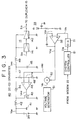
- FIG. 3 is a block diagram showing principal circuits of a portable telephone in the first embodiment of the invention.
- any like component elements corresponding to those in FIG. 1 are denoted by the same reference numerals or symbols, and a detailed description thereof is omitted.
- reference numeral 40 denotes a variable DC-DC converter which, in this embodiment, is based on chopper type switching.
- a capacitor 41 is connected in parallel to a battery 34, and a series circuit consisting of a coil 42 and the drain-source junction of an FET 43 is connected also in parallel to the battery 34. Further a series circuit consisting of a diode 44 and a capacitor 45 is connected in parallel to the drain-source junction of the FET 43. A terminal voltage V45 of the capacitor 45 is divided by resistors 47 and 48, and the divided voltage VTH is supplied as a reference voltage to a voltage comparator 46.
- terminal voltage V45 of the capacitor 45 is supplied via a high-frequency choke coil 49 to a power line of an amplifier 14.
- a voltage generator 51 As shown in FIG. 4A for example, the voltage generator 51 generates a sawtooth voltage V51 of a predetermined frequency. The voltage V51 thus generated is supplied to an adder 52, while the output signal of the voltage comparator 32 is supplied also to the adder 52. Then, as shown in FIG. 4A for example, the adder 52 produces an output voltage V52 which is the sum of the voltages V51 and V32 and is equal in DC level to the voltage V32.
- the voltage V52 is supplied to the comparator 46, whose comparison output voltage V46 is then supplied to the gate of the FET 43.
- the voltage V34 of the battery 34 is supplied to the coil 42 by way of the line consisting of the battery 34 ⁇ coil 42 ⁇ FET 43 ⁇ battery 34, so that the energy is stored in the coil 42. Meanwhile, when the FET 43 is turned off, the energy stored in the coil 42 is released to charge the capacitor 45 by way of the line consisting of the coil 42 ⁇ diode 44 ⁇ capacitor 45 ⁇ capacitor 41 and battery 34 ⁇ coil 42. Therefore a predetermined DC voltage V45 is obtained in the capacitor 45, and then the voltage V45 is supplied as an operating voltage to the amplifier 14 via a coil 49.
- the voltage V33 is lowered to consequently raise the voltage V32, thereby elongating the "H" duration of the PWM voltage V46.
- the on-time of the FET 43 is also elongated to consequently increase the energy stored in the coil 42, whereby the voltage V45 is raised to render the operating voltage of the amplifier 14 higher, hence increasing the transmission output.
- the transmission output of the amplifier 14 is increased, the voltage V33 is raised to consequently lower the voltage V32, thereby shortening the "H" duration of the PWM voltage V46.
- the "H" duration of the PWM voltage V46 is thus shortened, the on-time of the FET 43 is also shortened to eventually decrease the energy stored in the coil 42, whereby the voltage V45 is lowered to render the operating voltage of the amplifier 14 lower, hence reducing the transmission output.
- the efficiency can be kept at the maximum or proximate thereto regardless of the magnitude of the transmission output.
- the efficiency can be enhanced by 10 to 15 percent or so.
- the effect of enhancing the efficiency becomes greater in accordance with a reduction of the transmission output. Therefore, even under the conditions where the battery 34 is a lithium one and the output voltage V34 widely varies depending on the time of use, it is still possible to use the portable telephone for a long time properly without any harmful influence from the variation of the output voltage V34.
- the operating voltage V45 is produced by directly converting the output voltage V34 of the battery 34, by means of the chopper type variable DC-DC converter 40, into a value required for the amplifier 14. Therefore the amplifier 14 is capable of continuously minimizing the loss regardless of the operating voltage V45, and thus it becomes possible to attain a high efficiency from this point of view as well.
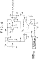
- FIG. 5 is a block diagram showing principal circuits of the portable telephone according to the second embodiment.
- any like component elements corresponding to those in FIG. 3 are denoted by the same reference numerals or symbols, and a detailed description thereof is omitted.
- the second embodiment shown in FIG. 5 represents an exemplary case of controlling the bias or gain of an amplifier 14 also in correspondence to the magnitude of a transmission output.
- data D61 of the value conforming to the MAC is extracted from an output port of a system controller 21 having a latch function.
- the data D61 is supplied to an D-A converter 61 where digital-to-analog conversion is executed to produce an analog voltage V61.
- the voltage V61 thus obtained is supplied to a voltage comparator 46 of a DC-DC converter 40 as a control voltage for the output voltage V45 similarly to the aforementioned voltage V52 in FIG. 3.
- the output voltage V32 of the comparator 32 is supplied to the amplifier 14 as a bias or gain control voltage, whereby the bias or gain of the amplifier 14 is controlled in response to the operating voltage V45 supplied to the amplifier 14.
- the operating voltage V45 of the amplifier 14 is controlled in response to the voltage V61 which is varied in accordance with the MAC, whereby the magnitude of the transmission output is controlled in conformity to the MAC.
- an enhanced efficiency is attainable in the case of a low-level transmission output as well as in the case of a high-level transmission output.
- the efficiency can be improved from this point of view as well.
- the amplifier 14 is enabled to perform a class-A or class-AB operation, no problem arises even if the signal S13 to be transmitted has any amplitude component. Therefore it is possible to apply the above to a portable telephone of digital cellular system where the transmission signal S13 is a QPSK signal or the like.
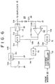
- FIG. 6 is a block diagram showing principal circuits in the third embodiment.
- any like component elements corresponding to those in FIG. 3 are denoted by the same reference numerals, and a detailed description thereof is omitted.
- a transmission signal S13 outputted from a transmitting circuit 13 is supplied via a variable attenuator 71 to a power amplifier 14, and a voltage V32 is supplied from a comparator 32 to the attenuator 71 as a control voltage thereof. And when a control action is so performed as to lower the operating voltage V45 of the amplifier 14 in response to the voltage V61, the level of the transmission signal S13 supplied from the attenuator 71 to the amplifier 14 is controlled in the polarity to lower the level of the signal S13.
- this third embodiment also, an enhanced efficiency is attainable in the case of a low-level transmission output as well as in the case of a high-level transmission output similarly to the aforementioned second embodiment of FIG. 5, and therefore it is possible to apply the third embodiment to a portable telephone of digital cellular system where the transmission signal S13 is a QPSK signal or the like.
- the output voltage V32 of the comparator 32 can be supplied as an operating voltage of the drive stage 141.
- similar effects can be achieved also in a transceiver or the like by applying the present invention thereto in a state where the magnitude of its transmission output is variable.
Landscapes
- Engineering & Computer Science (AREA)
- Power Engineering (AREA)
- Computer Networks & Wireless Communication (AREA)
- Signal Processing (AREA)
- Transmitters (AREA)
- Monitoring And Testing Of Transmission In General (AREA)
Applications Claiming Priority (3)
| Application Number | Priority Date | Filing Date | Title |
|---|---|---|---|
| JP5145508A JPH06334541A (ja) | 1993-05-25 | 1993-05-25 | 無線送信機 |
| JP14550893 | 1993-05-25 | ||
| JP145508/93 | 1993-05-25 |
Publications (2)
| Publication Number | Publication Date |
|---|---|
| EP0626765A1 true EP0626765A1 (fr) | 1994-11-30 |
| EP0626765B1 EP0626765B1 (fr) | 2002-01-02 |
Family
ID=15386877
Family Applications (1)
| Application Number | Title | Priority Date | Filing Date |
|---|---|---|---|
| EP94303630A Expired - Lifetime EP0626765B1 (fr) | 1993-05-25 | 1994-05-20 | Appareil de communication par radio |
Country Status (4)
| Country | Link |
|---|---|
| US (1) | US5604924A (fr) |
| EP (1) | EP0626765B1 (fr) |
| JP (1) | JPH06334541A (fr) |
| DE (1) | DE69429555T2 (fr) |
Cited By (9)
| Publication number | Priority date | Publication date | Assignee | Title |
|---|---|---|---|---|
| EP0851577A1 (fr) * | 1996-12-30 | 1998-07-01 | Alcatel | Dispositif d'alimentation d'un amplificateur de puissance pour terminal de radiocommunications mobiles |
| EP0940910A1 (fr) * | 1998-03-03 | 1999-09-08 | Robert Bosch Gmbh | Amplificateur de puissance pour un émetteur radio et téléphone moile avec un émetteur radio |
| WO2000019603A1 (fr) * | 1998-09-25 | 2000-04-06 | Conexant Systems, Inc. | Appareil et procede pour ameliorer la linearite d'une boucle d'un systeme de commande de puissance |
| GB2347288A (en) * | 1998-12-25 | 2000-08-30 | Matsushita Electric Industrial Co Ltd | Large dynamic range transmitter power control for a CDMA mobile phone |
| WO2002101944A3 (fr) * | 2001-06-11 | 2004-02-12 | Rf Micro Devices Inc | Commande d'amplificateur de puissance |
| US6998919B2 (en) | 2003-10-22 | 2006-02-14 | Rf Micro Devices, Inc. | Temperature compensated power amplifier power control |
| US7330071B1 (en) | 2005-10-19 | 2008-02-12 | Rf Micro Devices, Inc. | High efficiency radio frequency power amplifier having an extended dynamic range |
| US7336127B2 (en) | 2005-06-10 | 2008-02-26 | Rf Micro Devices, Inc. | Doherty amplifier configuration for a collector controlled power amplifier |
| EP2388911A3 (fr) * | 2010-05-20 | 2012-03-28 | Lg Electronics Inc. | Terminal mobile et procédé de contrôle de la tension de fonctionnement d'un amplificateur de puissance |
Families Citing this family (32)
| Publication number | Priority date | Publication date | Assignee | Title |
|---|---|---|---|---|
| JPH0818500A (ja) * | 1994-06-30 | 1996-01-19 | Nec Corp | 携帯無線機 |
| JP3279938B2 (ja) * | 1996-10-31 | 2002-04-30 | 京セラ株式会社 | 無線装置の送信出力制御方式 |
| US6091942A (en) * | 1996-12-02 | 2000-07-18 | Motorola, Inc. | Self gain aligning circuit and method |
| US6148220A (en) | 1997-04-25 | 2000-11-14 | Triquint Semiconductor, Inc. | Battery life extending technique for mobile wireless applications |
| US6163706A (en) * | 1997-11-18 | 2000-12-19 | Conexant Systems, Inc. | Apparatus for and method of improving efficiency of transceivers in radio products |
| JPH11177349A (ja) * | 1997-12-16 | 1999-07-02 | Matsushita Electric Ind Co Ltd | 電力増幅器 |
| US6141538A (en) * | 1998-03-03 | 2000-10-31 | Northrop Grumman Corporation | Transmit detection circuit |
| KR100301805B1 (ko) * | 1998-06-12 | 2001-09-22 | 김영환 | 신호압축장치 |
| KR100357619B1 (ko) * | 1998-06-23 | 2003-01-15 | 삼성전자 주식회사 | 이동 통신단말기의 출력전력 제어장치 및 방법 |
| US6791419B1 (en) * | 1998-12-02 | 2004-09-14 | Ericsson, Inc. | Constant gain, constant phase RF power block |
| US6341219B1 (en) * | 1999-02-05 | 2002-01-22 | Agere Systems Guardian Corp. | Single-source automatic power control method and apparatus for frequency-diverse variable-gain stages of a CDMA cellular handset |
| US6377784B2 (en) | 1999-02-09 | 2002-04-23 | Tropian, Inc. | High-efficiency modulation RF amplifier |
| US6864668B1 (en) | 1999-02-09 | 2005-03-08 | Tropian, Inc. | High-efficiency amplifier output level and burst control |
| US6559722B1 (en) * | 1999-08-10 | 2003-05-06 | Anadigics, Inc. | Low bias current/temperature compensation current mirror for linear power amplifier |
| SE517622C2 (sv) * | 1999-12-17 | 2002-06-25 | Ericsson Telefon Ab L M | Anordning för att minska en linjedrivares effektförlust |
| US6366177B1 (en) | 2000-02-02 | 2002-04-02 | Tropian Inc. | High-efficiency power modulators |
| GB2368737B (en) * | 2000-10-31 | 2004-11-10 | Roke Manor Research | Method and apparatus for controlling an amplifier |
| US6677823B2 (en) | 2001-02-28 | 2004-01-13 | Andrew Corporation | Gain compensation circuit using a variable offset voltage |
| US6882130B2 (en) * | 2001-04-17 | 2005-04-19 | Matsushita Electric Industrial Co., Ltd. | Battery-driven electronic device and mobile communication apparatus |
| JP3838547B2 (ja) * | 2001-12-11 | 2006-10-25 | 株式会社ルネサステクノロジ | 高周波電力増幅回路用の電源装置 |
| US6624702B1 (en) * | 2002-04-05 | 2003-09-23 | Rf Micro Devices, Inc. | Automatic Vcc control for optimum power amplifier efficiency |
| US20040203984A1 (en) * | 2002-06-11 | 2004-10-14 | Tai-Her Yang | Wireless information device with its transmission power lever adjustable |
| US20040072554A1 (en) * | 2002-10-15 | 2004-04-15 | Triquint Semiconductor, Inc. | Automatic-bias amplifier circuit |
| US7010284B2 (en) | 2002-11-06 | 2006-03-07 | Triquint Semiconductor, Inc. | Wireless communications device including power detector circuit coupled to sample signal at interior node of amplifier |
| US20040070454A1 (en) * | 2002-10-15 | 2004-04-15 | Triquint Semiconductor, Inc. | Continuous bias circuit and method for an amplifier |
| EP1658671A1 (fr) * | 2003-06-16 | 2006-05-24 | Paragon Communications Ltd. | Procede et appareil de regulation dynamique de la tension d'alimentation d'un amplificateur de puissance |
| US7177370B2 (en) * | 2003-12-17 | 2007-02-13 | Triquint Semiconductor, Inc. | Method and architecture for dual-mode linear and saturated power amplifier operation |
| EP1612965A3 (fr) * | 2004-07-01 | 2012-01-04 | NEC Corporation | Sélecteur d'antenne |
| EP1708358A3 (fr) * | 2005-03-11 | 2006-12-06 | LG Electronics Inc. | Terminal de communication mobile à dispositif de tension de commande et méthode |
| US7477102B1 (en) * | 2006-03-17 | 2009-01-13 | Hrl Laboratories, Llc | High efficiency linear microwave power amplifier |
| KR101689602B1 (ko) * | 2010-05-20 | 2016-12-26 | 엘지전자 주식회사 | 이동 단말기 및 전력 증폭 모듈의 구동 전압 제어 방법 |
| KR101689603B1 (ko) * | 2010-05-20 | 2017-01-09 | 엘지전자 주식회사 | 이동 단말기 및 전력 증폭 모듈의 구동 전압 제어 방법 |
Citations (5)
| Publication number | Priority date | Publication date | Assignee | Title |
|---|---|---|---|---|
| US4654882A (en) * | 1984-04-19 | 1987-03-31 | Nec Corporation | Radio communication device and method of controlling transmitter output power |
| GB2199467A (en) * | 1986-10-29 | 1988-07-06 | Oki Electric Ind Co Ltd | Preventing overheating of a mobile radio transmitter |
| US5065450A (en) * | 1989-03-21 | 1991-11-12 | Tft, Inc. | Frequency modulated radio frequency broadcast network employing a synchronous frequency modulated booster system |
| US5126688A (en) * | 1990-03-20 | 1992-06-30 | Oki Electric Co., Ltd. | Power amplifying apparatus for wireless transmitter |
| US5193219A (en) * | 1989-08-18 | 1993-03-09 | Nec Corporation | Vehicular power booster circuitry for multi-level portable transceiver |
Family Cites Families (5)
| Publication number | Priority date | Publication date | Assignee | Title |
|---|---|---|---|---|
| JPH02246531A (ja) * | 1989-03-20 | 1990-10-02 | Fujitsu Ltd | 送信電力可変形送信機の送信断検出回路 |
| KR910007680B1 (ko) * | 1989-04-26 | 1991-09-30 | 삼성전자 주식회사 | 휴대용 이동 무선전화기의 rf 전력 레벨 제어회로 |
| FI87028C (fi) * | 1989-12-22 | 1992-11-10 | Nokia Mobile Phones Ltd | Metod foer att reglera effekt hos en spaenningsstyrd effektfoerstaerkare och koppling foer anvaendning i metoden |
| US5182527A (en) * | 1990-03-30 | 1993-01-26 | Oki Electric Industry Co., Ltd. | Power amplifying apparatus for wireless transmitter |
| US5307512A (en) * | 1991-06-03 | 1994-04-26 | Motorola, Inc. | Power control circuitry for achieving wide dynamic range in a transmitter |
-
1993
- 1993-05-25 JP JP5145508A patent/JPH06334541A/ja active Pending
-
1994
- 1994-05-03 US US08/237,151 patent/US5604924A/en not_active Expired - Fee Related
- 1994-05-20 DE DE69429555T patent/DE69429555T2/de not_active Expired - Fee Related
- 1994-05-20 EP EP94303630A patent/EP0626765B1/fr not_active Expired - Lifetime
Patent Citations (5)
| Publication number | Priority date | Publication date | Assignee | Title |
|---|---|---|---|---|
| US4654882A (en) * | 1984-04-19 | 1987-03-31 | Nec Corporation | Radio communication device and method of controlling transmitter output power |
| GB2199467A (en) * | 1986-10-29 | 1988-07-06 | Oki Electric Ind Co Ltd | Preventing overheating of a mobile radio transmitter |
| US5065450A (en) * | 1989-03-21 | 1991-11-12 | Tft, Inc. | Frequency modulated radio frequency broadcast network employing a synchronous frequency modulated booster system |
| US5193219A (en) * | 1989-08-18 | 1993-03-09 | Nec Corporation | Vehicular power booster circuitry for multi-level portable transceiver |
| US5126688A (en) * | 1990-03-20 | 1992-06-30 | Oki Electric Co., Ltd. | Power amplifying apparatus for wireless transmitter |
Cited By (15)
| Publication number | Priority date | Publication date | Assignee | Title |
|---|---|---|---|---|
| EP0851577A1 (fr) * | 1996-12-30 | 1998-07-01 | Alcatel | Dispositif d'alimentation d'un amplificateur de puissance pour terminal de radiocommunications mobiles |
| FR2758024A1 (fr) * | 1996-12-30 | 1998-07-03 | Alsthom Cge Alcatel | Dispositif d'alimentation d'un amplificateur de puissance pour terminal de radiocommunications mobiles |
| US5977833A (en) * | 1996-12-30 | 1999-11-02 | Alcatel | Power supply circuit for a power amplifier of a mobile radio communication terminal |
| EP0940910A1 (fr) * | 1998-03-03 | 1999-09-08 | Robert Bosch Gmbh | Amplificateur de puissance pour un émetteur radio et téléphone moile avec un émetteur radio |
| WO2000019603A1 (fr) * | 1998-09-25 | 2000-04-06 | Conexant Systems, Inc. | Appareil et procede pour ameliorer la linearite d'une boucle d'un systeme de commande de puissance |
| US6466772B1 (en) | 1998-09-25 | 2002-10-15 | Skyworks Solutions, Inc. | Apparatus and method for improving power control loop linearity |
| GB2347288B (en) * | 1998-12-25 | 2001-01-10 | Matsushita Electric Industrial Co Ltd | Transmission power control in radio communication |
| GB2347288A (en) * | 1998-12-25 | 2000-08-30 | Matsushita Electric Industrial Co Ltd | Large dynamic range transmitter power control for a CDMA mobile phone |
| US6675000B1 (en) | 1998-12-25 | 2004-01-06 | Matsushita Electric Industrial Co., Ltd. | Radio communication apparatus and transmission power control method therein |
| WO2002101944A3 (fr) * | 2001-06-11 | 2004-02-12 | Rf Micro Devices Inc | Commande d'amplificateur de puissance |
| US6998919B2 (en) | 2003-10-22 | 2006-02-14 | Rf Micro Devices, Inc. | Temperature compensated power amplifier power control |
| US7336127B2 (en) | 2005-06-10 | 2008-02-26 | Rf Micro Devices, Inc. | Doherty amplifier configuration for a collector controlled power amplifier |
| US7330071B1 (en) | 2005-10-19 | 2008-02-12 | Rf Micro Devices, Inc. | High efficiency radio frequency power amplifier having an extended dynamic range |
| EP2388911A3 (fr) * | 2010-05-20 | 2012-03-28 | Lg Electronics Inc. | Terminal mobile et procédé de contrôle de la tension de fonctionnement d'un amplificateur de puissance |
| US8406706B2 (en) | 2010-05-20 | 2013-03-26 | Lg Electronics Inc. | Mobile terminal and method of controlling a driving voltage of a power amplifier therein |
Also Published As
| Publication number | Publication date |
|---|---|
| EP0626765B1 (fr) | 2002-01-02 |
| JPH06334541A (ja) | 1994-12-02 |
| DE69429555T2 (de) | 2002-08-08 |
| DE69429555D1 (de) | 2002-02-07 |
| US5604924A (en) | 1997-02-18 |
Similar Documents
| Publication | Publication Date | Title |
|---|---|---|
| US5604924A (en) | Radio communication apparatus in which output power is controlled by pulse width modulation using a mobile attenuation code | |
| KR100312367B1 (ko) | 이동체통신장치및방법 | |
| RU2252483C2 (ru) | Способ и устройство усиления мощности передачи беспроводного телефона при пониженном энергопотреблении | |
| CN1164027C (zh) | 具有供电调整以控制相邻和相间信道功率的功率放大电路 | |
| US7193459B1 (en) | Power amplifier control technique for enhanced efficiency | |
| US6133792A (en) | Method and apparatus for preventing power amplifier saturation | |
| JP2005513943A (ja) | 電力増幅器 | |
| GB2301964A (en) | Active variable capacitance control of the input or output impedance of a power rf amplifier to improve efficiency | |
| US5524287A (en) | Radio communication apparatus | |
| EP1104119B1 (fr) | Emetteur avec reglage de la puissance de sortie | |
| US6025753A (en) | Method and apparatus for amplifying a signal | |
| US20010034217A1 (en) | System and method for selectively interconnecting amplifiers in a communications device | |
| EP1530303A1 (fr) | Commande de la puissance dans un système de communication mobile | |
| US7545217B1 (en) | System and method for improving power efficiency in GSM power amplifiers | |
| KR100508355B1 (ko) | 오디오 및 rf 증폭기용 공유 전원을 구비하는 휴대용무선 송수신기 | |
| CN100466482C (zh) | 移动通信终端和优化功率放大器的工作点的方法 | |
| JP4048589B2 (ja) | 携帯電話機の送信電力制御方式 | |
| JP2000295046A (ja) | 電力増幅器を有する電子機器 | |
| KR960009926B1 (ko) | 휴대용 전화기 및 휴대용 전화기의 전력 증폭기의 출력 전력 제어 방법 | |
| KR100251585B1 (ko) | 동작 전류의 감소를 위한 무선 단말기 및 그 제어 방법 | |
| KR20010104063A (ko) | 이동통신 단말기에서의 송신전력 제어장치 | |
| KR20010104057A (ko) | 이동통신 단말기에서의 pdm 신호를 이용한 송신전력제어장치 | |
| JPH05343929A (ja) | 電力増幅器 | |
| JPH11308125A (ja) | 無線端末装置 | |
| JPH0514255A (ja) | 無線送受信機 |
Legal Events
| Date | Code | Title | Description |
|---|---|---|---|
| PUAI | Public reference made under article 153(3) epc to a published international application that has entered the european phase |
Free format text: ORIGINAL CODE: 0009012 |
|
| AK | Designated contracting states |
Kind code of ref document: A1 Designated state(s): DE GB IT |
|
| 17P | Request for examination filed |
Effective date: 19950505 |
|
| 17Q | First examination report despatched |
Effective date: 19980907 |
|
| GRAG | Despatch of communication of intention to grant |
Free format text: ORIGINAL CODE: EPIDOS AGRA |
|
| GRAG | Despatch of communication of intention to grant |
Free format text: ORIGINAL CODE: EPIDOS AGRA |
|
| GRAH | Despatch of communication of intention to grant a patent |
Free format text: ORIGINAL CODE: EPIDOS IGRA |
|
| GRAH | Despatch of communication of intention to grant a patent |
Free format text: ORIGINAL CODE: EPIDOS IGRA |
|
| GRAA | (expected) grant |
Free format text: ORIGINAL CODE: 0009210 |
|
| REG | Reference to a national code |
Ref country code: GB Ref legal event code: IF02 |
|
| AK | Designated contracting states |
Kind code of ref document: B1 Designated state(s): DE GB IT |
|
| RIC1 | Information provided on ipc code assigned before grant |
Free format text: 7H 04B 1/40 A, 7H 04Q 7/20 B |
|
| REF | Corresponds to: |
Ref document number: 69429555 Country of ref document: DE Date of ref document: 20020207 |
|
| PLBE | No opposition filed within time limit |
Free format text: ORIGINAL CODE: 0009261 |
|
| STAA | Information on the status of an ep patent application or granted ep patent |
Free format text: STATUS: NO OPPOSITION FILED WITHIN TIME LIMIT |
|
| 26N | No opposition filed | ||
| PGFP | Annual fee paid to national office [announced via postgrant information from national office to epo] |
Ref country code: GB Payment date: 20030514 Year of fee payment: 10 |
|
| PGFP | Annual fee paid to national office [announced via postgrant information from national office to epo] |
Ref country code: DE Payment date: 20030529 Year of fee payment: 10 |
|
| PG25 | Lapsed in a contracting state [announced via postgrant information from national office to epo] |
Ref country code: GB Free format text: LAPSE BECAUSE OF NON-PAYMENT OF DUE FEES Effective date: 20040520 |
|
| PG25 | Lapsed in a contracting state [announced via postgrant information from national office to epo] |
Ref country code: DE Free format text: LAPSE BECAUSE OF NON-PAYMENT OF DUE FEES Effective date: 20041201 |
|
| GBPC | Gb: european patent ceased through non-payment of renewal fee |
Effective date: 20040520 |
|
| PG25 | Lapsed in a contracting state [announced via postgrant information from national office to epo] |
Ref country code: IT Free format text: LAPSE BECAUSE OF NON-PAYMENT OF DUE FEES;WARNING: LAPSES OF ITALIAN PATENTS WITH EFFECTIVE DATE BEFORE 2007 MAY HAVE OCCURRED AT ANY TIME BEFORE 2007. THE CORRECT EFFECTIVE DATE MAY BE DIFFERENT FROM THE ONE RECORDED. Effective date: 20050520 |