EP0628982A2 - Driving method for an electron beam emitting device - Google Patents
Driving method for an electron beam emitting device Download PDFInfo
- Publication number
- EP0628982A2 EP0628982A2 EP94114636A EP94114636A EP0628982A2 EP 0628982 A2 EP0628982 A2 EP 0628982A2 EP 94114636 A EP94114636 A EP 94114636A EP 94114636 A EP94114636 A EP 94114636A EP 0628982 A2 EP0628982 A2 EP 0628982A2
- Authority
- EP
- European Patent Office
- Prior art keywords
- electron beam
- emitting
- electrodes
- electron
- light
- Prior art date
- Legal status (The legal status is an assumption and is not a legal conclusion. Google has not performed a legal analysis and makes no representation as to the accuracy of the status listed.)
- Granted
Links
Images


Classifications
-
- H—ELECTRICITY
- H01—ELECTRIC ELEMENTS
- H01J—ELECTRIC DISCHARGE TUBES OR DISCHARGE LAMPS
- H01J1/00—Details of electrodes, of magnetic control means, of screens, or of the mounting or spacing thereof, common to two or more basic types of discharge tubes or lamps
- H01J1/02—Main electrodes
- H01J1/30—Cold cathodes, e.g. field-emissive cathode
- H01J1/316—Cold cathodes, e.g. field-emissive cathode having an electric field parallel to the surface, e.g. thin film cathodes
-
- B—PERFORMING OPERATIONS; TRANSPORTING
- B82—NANOTECHNOLOGY
- B82Y—SPECIFIC USES OR APPLICATIONS OF NANOSTRUCTURES; MEASUREMENT OR ANALYSIS OF NANOSTRUCTURES; MANUFACTURE OR TREATMENT OF NANOSTRUCTURES
- B82Y10/00—Nanotechnology for information processing, storage or transmission, e.g. quantum computing or single electron logic
-
- H—ELECTRICITY
- H01—ELECTRIC ELEMENTS
- H01J—ELECTRIC DISCHARGE TUBES OR DISCHARGE LAMPS
- H01J31/00—Cathode ray tubes; Electron beam tubes
- H01J31/08—Cathode ray tubes; Electron beam tubes having a screen on or from which an image or pattern is formed, picked up, converted, or stored
- H01J31/10—Image or pattern display tubes, i.e. having electrical input and optical output; Flying-spot tubes for scanning purposes
- H01J31/12—Image or pattern display tubes, i.e. having electrical input and optical output; Flying-spot tubes for scanning purposes with luminescent screen
- H01J31/123—Flat display tubes
- H01J31/125—Flat display tubes provided with control means permitting the electron beam to reach selected parts of the screen, e.g. digital selection
- H01J31/127—Flat display tubes provided with control means permitting the electron beam to reach selected parts of the screen, e.g. digital selection using large area or array sources, i.e. essentially a source for each pixel group
-
- H—ELECTRICITY
- H01—ELECTRIC ELEMENTS
- H01J—ELECTRIC DISCHARGE TUBES OR DISCHARGE LAMPS
- H01J31/00—Cathode ray tubes; Electron beam tubes
- H01J31/08—Cathode ray tubes; Electron beam tubes having a screen on or from which an image or pattern is formed, picked up, converted, or stored
- H01J31/10—Image or pattern display tubes, i.e. having electrical input and optical output; Flying-spot tubes for scanning purposes
- H01J31/12—Image or pattern display tubes, i.e. having electrical input and optical output; Flying-spot tubes for scanning purposes with luminescent screen
- H01J31/15—Image or pattern display tubes, i.e. having electrical input and optical output; Flying-spot tubes for scanning purposes with luminescent screen with ray or beam selectively directed to luminescent anode segments
-
- H—ELECTRICITY
- H01—ELECTRIC ELEMENTS
- H01J—ELECTRIC DISCHARGE TUBES OR DISCHARGE LAMPS
- H01J2201/00—Electrodes common to discharge tubes
- H01J2201/30—Cold cathodes
- H01J2201/316—Cold cathodes having an electric field parallel to the surface thereof, e.g. thin film cathodes
- H01J2201/3165—Surface conduction emission type cathodes
Definitions
- This invention relates to a method for driving an electron beam emitting device as defined in the preamble clause of claim 1 and to a method for driving an image displaying device as defined in the preamble clause of claim 3.
- thin type image displaying device with good visual recognition has been demanded.
- liquid crystal displaying device for example, liquid crystal displaying device, EL displaying device, plasma display panel, etc.
- these involve problems in visual angle, color formation, luminosity, etc., and they cannot be said to satisfy the performances demanded by the market under the present situation.
- an electron beam emitting device comprising a surface conduction type of thin film device having an electron emitting area and a pair of electrodes for passing current through the electron emitting area, and being characterized by a voltage applying means for applying independent voltage on each of said electrodes so that each of said electrodes may become higher or lower in potential relative to the other electrode.
- Said own proposal being also directed to an image displaying device comprising such an electron beam emitting device and at least one light emitting member which draws an image by emitting light when irradiated by an electron beam emitted from said electron beam emitting device.
- the present invention is directed to a driving method for an electron beam emitting device and an image displaying device in particular of the type as defined in the said own proposal.
- the invention consists in a driving method of an electron beam emitting device comprising a surface conduction type of thin film device having an electron emitting area and a pair of electrodes for passing current through the electron emitting area, characterized in that a track of the emitted electron beam is varied by varying a value of a voltage applied between said pair of electrodes.
- the invention consists in a driving method of an image displaying device comprising an electron beam emitting device comprising a surface conduction type of thin film device having an electron emitting area and a pair of electrodes for passing current through the electron emitting area, and a light-emitting member which is irradiated with the electron beam from said electron beam emitting device to form a light-emitting image, characterized in that a track of the emitted electron beam is varied by varying a value of a voltage applied between said pair of electrodes, so that a site to be irradiated with the electron beam in said light-emitting member is shifted.
- a surface conduction type of thin film device is used as the electron beam emitting source, and for the surface conduction type of thin film device itself, all of those known in the art can be utilized, and its device constitution and shape are not particularly limited, so long as they do not interfere with the function of the device according to the present invention.
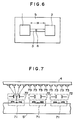
- FIG. 6 An example of the surface conduction type of thin film device to be used in the present invention is shown in Fig. 6.
- 1 and 2 are electrodes for obtaining electrical connection
- 3 is a thin film formed of an electron emitting material
- 5 shows a substrate and 4 an electron emitting area.
- the method for forming the electron emitting area 4 for example, there may be included the method according to current passage heat treatment called forming in which current is passed through the thin film 3 by applying voltage between the above electrodes 1 and 2 to destroy, deform or denature locally the thin film 3 with Joule's heat generated thereby, thus forming an electron emitting area 4 made to electrically high resistant state to obtain electron emitting function, or the method to obtain electron emitting function without passing through the forming step by dispersion arrangement of fine particles comprising a metal or oxide, etc. at the fine interval portion 3 between a pair of confronting electrodes 1, 2 having a fine interval, but these methods are not limitative of the invention, the electron emitting area may be formed according to any method, provided that sufficient electron discharge can be realized.
- the substrate 5 in the surface conduction type of thin film device to be used in the present invention for example, an insulating material such as glass, quartz, etc. may be employed.
- the thickness of the substrate may be about some 100 ⁇ m to 1 mm, and when it is used also as the back plate as described below, a thickness of around 5 mm may be preferred.
- the electrodes 1 and 2 can be formed according to, for example, the methods conventionally employed in vacuum vapor deposition process and photolithographic process, etc.
- the materials for the electrodes 1 and 2 may be general electroconductive materials, including metals such as Ni, Al, Cu, Au, Pt, Ag, etc. and metal oxides such as SnO2, ITO, etc.
- the thickness of the electrode may be suitably some 10 nm (100 ⁇ ) to several ⁇ m, preferably 0.01 to 2 ⁇ m.
- the interval between the electrodes 1 and 2, namely the electrode gap H may be from 0.1 ⁇ m to several ⁇ m, but the present invention is not limited thereto.
- electrodes 1 and 2 As to the shape of electrodes 1 and 2, it is not particularly limited, provided that electron discharge with good efficiency can be realized.
- Formation of the electron emitting area 4 between the electrodes 1 and 2 can be practiced by forming the thin film 3 according to vacuum deposition, etc. by use of an electron emitting material, for example, a metal oxide such as In2O3, SnO2, PbO, etc. a metal such as Ag, Pt, Al, Cu, Au, etc., carbon and other various semiconductors, etc. and applying forming treatment thereto similarly as in the prior art.
- an electron emitting material for example, a metal oxide such as In2O3, SnO2, PbO, etc. a metal such as Ag, Pt, Al, Cu, Au, etc., carbon and other various semiconductors, etc. and applying forming treatment thereto similarly as in the prior art.
- the electron emitting area 4 there may be also employed the method in which a dispersion containing fine particles of the above electron emitting material dispersed in a dispersing medium is coated on the substrate by dipping or spin coating, etc., followed by calcination.
- a dispersing medium any medium capable of dispersing fine particles without denaturation, such as butyl acetate, alcohols, methyl ethyl ketone, cyclohexane and mixtures of these, etc.
- the fine particles should have particle sized preferably of some nm (10 ⁇ ) to several ⁇ m.
- the electron beam emitting device of the present invention generates electron beam by applying voltage between the electrodes 1 and 2 of the above surface conduct ion type of thin film device, thereby passing current through the electron emitting area 4, and such means for applying voltage can apply voltage so that, for example, the electrode 1 may be higher or lower in potential relative to the electrode 2. That is, the first specific feature resides in that the direction of current flowing through the electron emitting area 4 can be reversed at any suitable time from the electrode 1 ⁇ 2 direction to the electrode 2 ⁇ 1 direction, and further the second specific feature of the above means for applying voltage resides in that the voltage applied between the electrodes 1 and 2 can be made variable.
- 1 and 2 are electrodes provided for applying voltage
- 3 is a thin film of a material such as metal or metal oxide as described above (depending on the material of the thin film 3, the same material as electrodes 1 and 2 may be also used)
- 4 is an electron emitting area formed by applying treatment called forming known in the art on the above thin film 3
- 5 is a substrate.
- 51 is the collector electrode for capturing electron beam discharged from the device and is coated on the surface with an organic resist for recording the site on which the electron beam is irradiated.
- the present invention has been accomplished on the basis of the experimental results as described above.
- the displacement amount ⁇ x by the applied voltage Vf will vary depending on the surface or size of the surface conduction type of thin film device, the material to be used for the thin film 3, the distance between the device and the collector electrode, the applied voltage Va at the collector electrode, etc., but the present invention is applicable to any case.
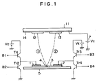
- Fig. 1 is a partial illustration showing an embodiment of the image displaying device of the present invention, which shows on of a large number of displaying units constituting the image displaying device.
- 1 to 4 are the same as in Fig. 5 as described above, showing the respective parts of the surface conduction type of thin film device.
- 5 and 11 consist of glass members shaped in plates, and constitute the back plate 5 and the face plate 11 of the image displaying device.
- a vacuum vessel is formed by the above back plate 5, the face plate 11 and side plates (not shown), and is internally maintained at a vacuum degree of around 1.33 ⁇ 10 ⁇ 4Pa (1 x 10 ⁇ 6 torr).
- light emitting members 12 and 13 are coated separately in mosaic with a transparent electrode 14 sandwiched therebetween.
- the specific feature resides in reversing the voltage polarity applied between the electrodes of the surface conduction type of thin film device at any suitable time, namely reversing the direction of the current flowing through the electron emitting area 4 by applying a voltage between the electrodes 1 and 2 so that, for example, the electrode 1 may be higher or lower in potential relative to the electrode 2, and Tr1, Tr2, Tr3 and Tr4 shown in the Figure are transistors of the switching device for that purpose.
- the transistors Tr1 and Tr2 control the voltage applied on the electrode 1, while the transistors Tr3 and Tr4 control the voltage applied on the electrode 2. ON or OFF of switching of each transistor can be controlled externally through the base terminals B1 to B4.
- one of the light emitting members 12 or 13 can be lighted selectively, or by repeating alternately the states (i) and (ii) for about 60 times per second, both picture elements can be displayed as if lighted in visual effect.
- the display units shown in the above Fig. 1 were juxtaposed in number of 200 x 200 in the vacuum vessel. By driving each unit independently, display of 200 x 400 picture elements is possible, which is very suitable for display of letters or figures.
- the thickness of the device is as thin as about 3 cm.
- Fig. 1 display of high luminance can be obtained with a very simple structure. Therefore, an information instrument terminal dealing with, for example, letters or figures can be provided at low cost.
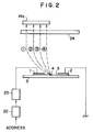
- Fig. 2 As the unit of the electron beam emitting device of the present invention, it is also possible to use the form shown in Fig. 2 in combination.
- Fig. 2 As the voltage to be applied on the surface conduction type of thin film device, the four kinds of combinations shown in Table 2 can be used, whereby a desired track of 1 to 4 can be selected.
- Table 2 Electron Track Applied Voltage at the electrode 1 Applied Voltage at the electrode 2 1 V1 0 2 V2 0 3 V3 0 4 V4 0 Note ... V1>V2>V3>V4>0
- a D/A converter 23 and a memory 22 may be also provided as shown in Fig. 2.
- the voltage to be applied on the electrode 1 is previously memoried in order to fly electron beams along the respective tracks of 1 to 4, and the data are set so as to be output to the D/A converter 23 by designating the address externally.
- the D/A converter 23 is set so as to generate the voltage based on the numerical data output from the memory 22.
- Fig. 3 shows the embodiment in which the form shown in Fig. 2 is used in combination with the form shown in Fig. 1.
- Fig. 3 1 to 5, 7, 11 and14 have the same constitutions as shown above in Fig. 1, but in this embodiment, for the electrodes 1 and 2, memories 31 and 33, D/A converters 30 and 32 are provided, respectively.
- memories 31 and 33 D/A converters 30 and 32 are provided, respectively.
- V1, V2, V3, V4 and 0[V] By designating addresses externally to the memories 31 and 32, five potentials V1, V2, V3, V4 and 0[V] (with proviso V1>V2>V3>V4>0) can be selectively applied on the electrodes 1 and 2.
- the track of electron beam can be selected from among 1 to 8 as shown in the Table 3 below.
- Fig. 3 which has a means for reversing the direction of current flowing through the electron emitting area at any suitable time by applying a potential difference between the both electrodes so that each electrode may be higher or lower in potential than the other electrode as shown in Fig. 1 and a means for changing the potential difference applied between the both electrodes at any suitable time as shown in Fig. 2 in combination, two or more picture element displays are possible for one electron emitting device are possible.
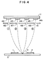
- the unit of the displaying device of the present invention the form shown in Fig. 4 can be employed.
- one desired picture element is the light emitting members 42 to 45 can be permitted to emit light.
- Table 4 Electron Track Applied Voltage at the electrode 1 Applied Voltage at the electrode 2 1 V1 0 2 V2 0 3 0 V2 4 0 V1 Note ... V1>V2>0
- a plate electrode 41 is held between the surface conduction type of thin film device and the light emitting member. Said plate electrode 41 is provided with holes 46 to 49 for permitting electron beam to transmit therethrough.
- Said plate electrode 41 is applied with a voltage lower than the voltage Va (voltage applied on the transparent electrode 14b), and the following effects can be obtained by selecting an appropriate voltage:
- a displaying device since deflection of electron beam is possible without provision of a deflector at the electron beam emitting source, a displaying device can be obtained with an extremely simple structure.
Landscapes
- Engineering & Computer Science (AREA)
- Chemical & Material Sciences (AREA)
- Nanotechnology (AREA)
- Physics & Mathematics (AREA)
- Mathematical Physics (AREA)
- Theoretical Computer Science (AREA)
- Crystallography & Structural Chemistry (AREA)
- Cathode-Ray Tubes And Fluorescent Screens For Display (AREA)
- Electrodes For Cathode-Ray Tubes (AREA)
- Cold Cathode And The Manufacture (AREA)
Abstract
Description
- This invention relates to a method for driving an electron beam emitting device as defined in the preamble clause of
claim 1 and to a method for driving an image displaying device as defined in the preamble clause ofclaim 3. - In recent years, in the field of information instruments or TV receiver for domestic use, thin type image displaying device with good visual recognition has been demanded. In the prior art, as thin type image displaying device, there have been developed, for example, liquid crystal displaying device, EL displaying device, plasma display panel, etc., but these involve problems in visual angle, color formation, luminosity, etc., and they cannot be said to satisfy the performances demanded by the market under the present situation.
- Whereas, in the prior art, as the device capable of obtaining emission of electrons with a simple structure, there has been known, for example, the cold cathode-ray device reported by M.I. Elinson [Radio Eng. Electron. Phys. vol. 10, 1290 - 1296, 1965]. This utilizes the phenomenon that electron emission occurs by passing current through the thin film with small area formed on a substrate in parallel to the thin surface, and is generally called the surface conduct ion type of thin film device.
- As such surface conduction type of thin film device, one by use of the SnO₂(Sb) thin film developed by Elinson et al as mentioned above; one by use of Au thin film [G. Dittmer: "Thin Solid Films", vol. 9, p. 317, 1972]; one by use of ITO film [M. Harwell and C.G. Fonstad: "IEEE Trans. ED Conf.", p. 519, 1975]; and one by use of carbon thin film [Hisashi Araki et al: "Vacuum", vol. 26, No. 1, p. 22, 1983] have been reported.
- These surface conduction type devices have the following advantages:
- 1) High electron emitting efficiency can be obtained.
- 2) Simple structure affords easy production.
- 3) A large number of devices can be formed (multi-formation) on the same substrate.
- Accordingly, if these surface conduction type of thin film devices can be utilized as the electron generating source for the flat plate type CRT image displaying device, an image displaying device more excellent in visual angle, color formation, luminosity and further in low consumption power, etc. as compared with the flat plate type CRT displaying device can be provided.
- However, when the surface conduction type of thin film device is attempted to be utilized for the electron generating source of an image displaying device, if the surface conduction type of thin film devices are provided in the same number as the displaying picture elements for excitation of phosphor, the number of the devices will become enormous, whereby the production yield will be lowered to result in increased cost. On the other hand, if the whole image surface is scanned by use of a single device, the device constitution will become complicated similarly as in the case of CRT of the prior art, as suggested in US-A-36 11 077, whereby it impossible to realize thinning of the device.
- Accordingly, as an idea of compromise, if some picture elements to some 10 picture elements are allocated for one device, it becomes possible to ballance well both the production yield of the device and thinning of the device at high level. However, even in that case, for scanning of electron beam, deflectors are required to be equipped for each device, and yet the deflector of the prior art had a complicated electrode shape as shown in Fig. 7, and therefore it has been difficult to make it fine or constitute them in multiple forms. In the Figure, 71 encircled with dotted line shows one device of the surface conduction type discharging device, 72 encircled similarly with dotted line shows one deflector, 73 is one picture element of emitting member and 74 is a glass plate.
- According to an own proposal in EP-A-312 007 (Application Number 88 116 926.2), the grant thereof being imminent, and from which the present application has been divided out, the aforementioned needs have been met by an electron beam emitting device comprising a surface conduction type of thin film device having an electron emitting area and a pair of electrodes for passing current through the electron emitting area, and being characterized by a voltage applying means for applying independent voltage on each of said electrodes so that each of said electrodes may become higher or lower in potential relative to the other electrode. Said own proposal being also directed to an image displaying device comprising such an electron beam emitting device and at least one light emitting member which draws an image by emitting light when irradiated by an electron beam emitted from said electron beam emitting device.
- The present invention is directed to a driving method for an electron beam emitting device and an image displaying device in particular of the type as defined in the said own proposal.
- Accordingly, the invention consists in a driving method of an electron beam emitting device comprising a surface conduction type of thin film device having an electron emitting area and a pair of electrodes for passing current through the electron emitting area, characterized in that a track of the emitted electron beam is varied by varying a value of a voltage applied between said pair of electrodes.
- Furthermore, the invention consists in a driving method of an image displaying device comprising an electron beam emitting device comprising a surface conduction type of thin film device having an electron emitting area and a pair of electrodes for passing current through the electron emitting area, and a light-emitting member which is irradiated with the electron beam from said electron beam emitting device to form a light-emitting image, characterized in that a track of the emitted electron beam is varied by varying a value of a voltage applied between said pair of electrodes, so that a site to be irradiated with the electron beam in said light-emitting member is shifted.
-
- Fig. 1 is a partial illustration showing an embodiment of the image displaying device of the present invention;
- Fig. 2, Fig. 3 and Fig. 4 are partial illustrations showing other embodiments of the displaying device;
- Fig. 5A, Fig. 5B and Fig. 6 are illustrations showing the constitution of the surface conduction type of thin film device; and
- Fig. 7 is an illustration of the image displaying device by use of the surface conduction type of thin film device of the prior art.
- In the present invention, a surface conduction type of thin film device is used as the electron beam emitting source, and for the surface conduction type of thin film device itself, all of those known in the art can be utilized, and its device constitution and shape are not particularly limited, so long as they do not interfere with the function of the device according to the present invention.
- An example of the surface conduction type of thin film device to be used in the present invention is shown in Fig. 6. In Fig. 6, 1 and 2 are electrodes for obtaining electrical connection, 3 is a thin film formed of an electron emitting material, 5 shows a substrate and 4 an electron emitting area.
- In the above surface conduction type of thin film device, as the method for forming the
electron emitting area 4, for example, there may be included the method according to current passage heat treatment called forming in which current is passed through thethin film 3 by applying voltage between theabove electrodes thin film 3 with Joule's heat generated thereby, thus forming anelectron emitting area 4 made to electrically high resistant state to obtain electron emitting function, or the method to obtain electron emitting function without passing through the forming step by dispersion arrangement of fine particles comprising a metal or oxide, etc. at thefine interval portion 3 between a pair of confrontingelectrodes - Further, for the
substrate 5 in the surface conduction type of thin film device to be used in the present invention, for example, an insulating material such as glass, quartz, etc. may be employed. The thickness of the substrate may be about some 100 µm to 1 mm, and when it is used also as the back plate as described below, a thickness of around 5 mm may be preferred. - The
electrodes electrodes - The thickness of the electrode may be suitably some 10 nm (100 Å) to several µm, preferably 0.01 to 2 µm.
- The interval between the
electrodes - As to the shape of
electrodes - Formation of the
electron emitting area 4 between theelectrodes thin film 3 according to vacuum deposition, etc. by use of an electron emitting material, for example, a metal oxide such as In₂O₃, SnO₂, PbO, etc. a metal such as Ag, Pt, Al, Cu, Au, etc., carbon and other various semiconductors, etc. and applying forming treatment thereto similarly as in the prior art. - As another method for forming the
electron emitting area 4, there may be also employed the method in which a dispersion containing fine particles of the above electron emitting material dispersed in a dispersing medium is coated on the substrate by dipping or spin coating, etc., followed by calcination. As the dispersing medium in this case, any medium capable of dispersing fine particles without denaturation, such as butyl acetate, alcohols, methyl ethyl ketone, cyclohexane and mixtures of these, etc. The fine particles should have particle sized preferably of some nm (10 Å) to several µm. - The electron beam emitting device of the present invention generates electron beam by applying voltage between the
electrodes electron emitting area 4, and such means for applying voltage can apply voltage so that, for example, theelectrode 1 may be higher or lower in potential relative to theelectrode 2. That is, the first specific feature resides in that the direction of current flowing through theelectron emitting area 4 can be reversed at any suitable time from theelectrode 1 → 2 direction to theelectrode 2 → 1 direction, and further the second specific feature of the above means for applying voltage resides in that the voltage applied between theelectrodes - Prior to completion of the present invention, the present inventors have experimentally confirmed that there is the relationship as shown in Fig. 5 between the voltage applied between the two electrodes and the track of electron beam in the surface conduction type releasing device.
- In Figs. 5A and 5B, 1 and 2 are electrodes provided for applying voltage, 3 is a thin film of a material such as metal or metal oxide as described above (depending on the material of the
thin film 3, the same material aselectrodes thin film - Also, 51 is the collector electrode for capturing electron beam discharged from the device and is coated on the surface with an organic resist for recording the site on which the electron beam is irradiated.
- According to the experiments conducted by the present inventors, as shown in the same Figure 5A, when a constant voltage Va was applied-on the
collector electrode 51 and a voltage Vf between theelectrodes exposure point 52 of the resist was found to be at a position deviated toward the side of theelectrode 2 than the normal line (broken line) of theelectron emitting area 4. Besides, when the voltage Vf was varied at constant voltage of Va, it has been found that the displacement amount Δx₁ becomes greater as the voltage Vf is made greater. Also, as shown in the same Figure 5B, when the polarity of voltage applied between theelectrodes exposure point 52 was transferred to the side of theelectrode 1, and similarly as in the case of Fig. 5A, the displacement amount Δx₂ became greater as the Vf was made greater. - The present invention has been accomplished on the basis of the experimental results as described above. The displacement amount Δx by the applied voltage Vf will vary depending on the surface or size of the surface conduction type of thin film device, the material to be used for the
thin film 3, the distance between the device and the collector electrode, the applied voltage Va at the collector electrode, etc., but the present invention is applicable to any case. - The present invention is described in more detail by referring to the drawings.
- Fig. 1 is a partial illustration showing an embodiment of the image displaying device of the present invention, which shows on of a large number of displaying units constituting the image displaying device. In the Figure, 1 to 4 are the same as in Fig. 5 as described above, showing the respective parts of the surface conduction type of thin film device. 5 and 11 consist of glass members shaped in plates, and constitute the
back plate 5 and the face plate 11 of the image displaying device. A vacuum vessel is formed by theabove back plate 5, the face plate 11 and side plates (not shown), and is internally maintained at a vacuum degree of around 1.33·10⁻⁴Pa (1 x 10⁻⁶ torr). On the inner surface of the face plate 11,light emitting members transparent electrode 14 sandwiched therebetween. - On the above transparent electrode is applied from the high
voltage power source 7 an acceleration voltage of, for example. Vc=10 kV. - In the image displaying device of this embodiment, the specific feature resides in reversing the voltage polarity applied between the electrodes of the surface conduction type of thin film device at any suitable time, namely reversing the direction of the current flowing through the
electron emitting area 4 by applying a voltage between theelectrodes electrode 1 may be higher or lower in potential relative to theelectrode 2, and Tr1, Tr2, Tr3 and Tr4 shown in the Figure are transistors of the switching device for that purpose. The transistors Tr1 and Tr2 control the voltage applied on theelectrode 1, while the transistors Tr3 and Tr4 control the voltage applied on theelectrode 2. ON or OFF of switching of each transistor can be controlled externally through the base terminals B1 to B4. - In the present device, there exist the three actuation states, namely:
- (i) the electron beam emitted from the surface conduction type of thin film device flies along the track shown by ① in Fig. 1, whereby the
light emitting member 12 emits light; - (ii) the electron beam emitted from the surface conduction type of thin film device flies along the track shown by ② in Fig. 1 (2), whereby the
light emitting member 13 emits light; and - (iii) the surface conduction type device is not driven, whereby the electron beam becomes OFF to effect no emission.
- It is determined by the actuations of the transistors Tr1 to Tr4 as shown in Table 1 whether either actuation state among these is taken.
Table 1 Electron Beam ①Electron Beam ②Electron Beam OFF Tr1 ○ X X Tr2 X ○ ○ Tr3 X ○ X Tr4 ○ X ○ Note ...
○ : Transistor ON
X : Transistor OFF - For example, when the transistors Tr1 and Tr4 are ON, Tr2 and Tr3 are OFF, VE[V] is applied on the
electrode 1 and 0[V] on theelectrode 2 in Fig. 1, whereby the electron beams flies along thetrack ①, as apparently seen from the description for Fig. 5B as described above (actuation state (i)). - When the transistors Tr2 and Tr3 are ON, Tr1 and Tr4 are OFF, the voltages applied on the
electrode 1,electrode 2 are reversed, whereby the electron beam is deflected toward theelectrode 2 side and flies along the track ② (actuation state (ii)). - On the other hand, when the transistors Tr2 and Tr4 are ON, Tr1 and Tr3 are OFF, since 0[V] is applied on both of the
electrode 1 and theelectrode 2, no electron emission will occur (actuation state (iii)). - Accordingly, by applying an appropriate signal on the base terminals B1 to B4, one of the
light emitting members - In the image displaying device practically prepared by the present inventors, the display units shown in the above Fig. 1 were juxtaposed in number of 200 x 200 in the vacuum vessel. By driving each unit independently, display of 200 x 400 picture elements is possible, which is very suitable for display of letters or figures.
- Besides, while having a luminance of 342.5 cd/m² (100 [ft-L]), the thickness of the device is as thin as about 3 cm.
- Thus, according to Fig. 1, display of high luminance can be obtained with a very simple structure. Therefore, an information instrument terminal dealing with, for example, letters or figures can be provided at low cost.
- As the unit of the electron beam emitting device of the present invention, it is also possible to use the form shown in Fig. 2 in combination. First, in Fig. 2, as the voltage to be applied on the surface conduction type of thin film device, the four kinds of combinations shown in Table 2 can be used, whereby a desired track of ① to ④ can be selected.
Table 2 Electron Track Applied Voltage at the electrode 1Applied Voltage at the electrode 2① V1 0 ② V2 0 ③ V3 0 ④ V4 0 Note ... V1>V2>V3>V4>0 - Also, by varying continuously the applied voltage, it is also possible to draw a line continuous through the
electrode 24 withdrawing the electrons emitted from theelectron emitting area 4 onto the target. - Further, in the image displaying device of the present invention, a D/
A converter 23 and amemory 22 may be also provided as shown in Fig. 2. In this case, within thememory 22, the voltage to be applied on theelectrode 1 is previously memoried in order to fly electron beams along the respective tracks of ① to ④, and the data are set so as to be output to the D/A converter 23 by designating the address externally. - The D/
A converter 23 is set so as to generate the voltage based on the numerical data output from thememory 22. - Fig. 3 shows the embodiment in which the form shown in Fig. 2 is used in combination with the form shown in Fig. 1.
- In Fig. 3, 1 to 5, 7, 11 and14 have the same constitutions as shown above in Fig. 1, but in this embodiment, for the
electrodes memories A converters memories electrodes Table 3 Electron Track Applied Voltage at the electrode 1Applied Voltage at the electrode 2① V1 0 ② V2 0 ③ V3 0 ④ V4 0 ⑤ 0 V1 ⑥ 0 V2 ⑦ 0 V3 ⑧ 0 V4 Non-lighting 0 0 - In the image displaying device of the present invention shown in Fig. 3, which has a means for reversing the direction of current flowing through the electron emitting area at any suitable time by applying a potential difference between the both electrodes so that each electrode may be higher or lower in potential than the other electrode as shown in Fig. 1 and a means for changing the potential difference applied between the both electrodes at any suitable time as shown in Fig. 2 in combination, two or more picture element displays are possible for one electron emitting device are possible.
- Also, as the unit of the displaying device of the present invention, the form shown in Fig. 4 can be employed. In the case of this device, by use of the four kinds of combinations shown in Table 4, one desired picture element is the
light emitting members 42 to 45 can be permitted to emit light.Table 4 Electron Track Applied Voltage at the electrode 1Applied Voltage at the electrode 2① V1 0 ② V2 0 ③ 0 V2 ④ 0 V1 Note ... V1>V2>0 - In the case of this embodiment, a
plate electrode 41 is held between the surface conduction type of thin film device and the light emitting member. Saidplate electrode 41 is provided withholes 46 to 49 for permitting electron beam to transmit therethrough. - Said
plate electrode 41 is applied with a voltage lower than the voltage Va (voltage applied on thetransparent electrode 14b), and the following effects can be obtained by selecting an appropriate voltage: - (a) Through the lens effect, electron beam is narrowed at the light emitting member surface, and therefore the emitting spot becomes sharp.
- (b) Deflection sensitivity becomes greater. That is, as compared with the case when no
plate electrode 41 is provided, deflection of electron beam becomes possible with smaller voltage (V1, V2). - As described above, according to the present invention, since deflection of electron beam is possible without provision of a deflector at the electron beam emitting source, a displaying device can be obtained with an extremely simple structure.
- As the result, in spite of having the same high luminosity as CRT of the prior art, a displaying device with a thickness which can be less than half of that of CRT of the prior art can be provided at low cost.
Claims (8)
- A driving method of an electron beam emitting device comprising a surface conduction tape of thin film device having an electron emitting area and a pair of electrodes for passing current through the electron emitting area,
characterized in that
a track of the emitted electron beam is varied by varying a value of a voltage applied between said pair of electrodes. - A method according to claim 1, wherein
the voltage value which accomplishes a desired track of an emitted electron beam is selected among data consisting of values of plural voltages associated with the different electron beam tracks, and the selected voltage value is applied between the pair of electrodes. - A method according to claim 1 or 2, therein
electron beam emitting devices are arranged in a plural number along plural columns and rows. - A driving method of an image displaying device comprising an electron beam emitting device comprising a surface conduction type of thin film device having an electron emitting area and a pair of electrodes for passing current through the electron emitting area, and a light-emitting member which is irradiated with the electron beam from said electron beam emitting device to form a light-emitting image,
characterized in that
a track of the emitted electron beam is varied by varying a value of a voltage applied between said pair of electrodes, so that a site to be irradiated with the electron beam in said light-emitting member is shifted. - A method according to claim 4 , wherein
the voltage value which accomplishes a desired track of an emitted electron beam is selected among data consisting of values of plural voltages associated with the different electron beam tracks, and the selected voltage value is applied between the pair of electrodes, so that a site to be irradiated with the electron beam in said light-emitting member is shifted. - A method according to claim 4 or 5, wherein said site is at least one picture element to be irradiated with the electron beam in said light-emitting member.
- A method according to claim 4 or 5, wherein said electron beam emitting devices are arranged in a plural number a long plural columns and rows.
- A method according to claim 4 or 5, wherein said light emitting members are arranged in a plural number along plural columns and rows.
Applications Claiming Priority (3)
| Application Number | Priority Date | Filing Date | Title |
|---|---|---|---|
| JP25455787A JP2622842B2 (en) | 1987-10-12 | 1987-10-12 | Electron beam image display device and deflection method for electron beam image display device |
| JP254557/87 | 1987-10-12 | ||
| EP88116926A EP0312007B1 (en) | 1987-10-12 | 1988-10-12 | Electron beam emitting device and image displaying device by use thereof |
Related Parent Applications (2)
| Application Number | Title | Priority Date | Filing Date |
|---|---|---|---|
| EP88116926.2 Division | 1988-10-12 | ||
| EP88116926A Division EP0312007B1 (en) | 1987-10-12 | 1988-10-12 | Electron beam emitting device and image displaying device by use thereof |
Publications (3)
| Publication Number | Publication Date |
|---|---|
| EP0628982A2 true EP0628982A2 (en) | 1994-12-14 |
| EP0628982A3 EP0628982A3 (en) | 1995-03-01 |
| EP0628982B1 EP0628982B1 (en) | 1998-01-14 |
Family
ID=17266700
Family Applications (2)
| Application Number | Title | Priority Date | Filing Date |
|---|---|---|---|
| EP94114636A Expired - Lifetime EP0628982B1 (en) | 1987-10-12 | 1988-10-12 | Driving method for electron beam emitting devices |
| EP88116926A Expired - Lifetime EP0312007B1 (en) | 1987-10-12 | 1988-10-12 | Electron beam emitting device and image displaying device by use thereof |
Family Applications After (1)
| Application Number | Title | Priority Date | Filing Date |
|---|---|---|---|
| EP88116926A Expired - Lifetime EP0312007B1 (en) | 1987-10-12 | 1988-10-12 | Electron beam emitting device and image displaying device by use thereof |
Country Status (4)
| Country | Link |
|---|---|
| US (1) | US5155416A (en) |
| EP (2) | EP0628982B1 (en) |
| JP (1) | JP2622842B2 (en) |
| DE (2) | DE3856115T2 (en) |
Cited By (9)
| Publication number | Priority date | Publication date | Assignee | Title |
|---|---|---|---|---|
| US6208072B1 (en) | 1997-08-28 | 2001-03-27 | Matsushita Electronics Corporation | Image display apparatus with focusing and deflecting electrodes |
| US6236381B1 (en) | 1997-12-01 | 2001-05-22 | Matsushita Electronics Corporation | Image display apparatus |
| US6278235B1 (en) | 1997-12-22 | 2001-08-21 | Matsushita Electronics Corporation | Flat-type display apparatus with front case to which grid frame with extended electrodes fixed thereto is attached |
| US6320310B1 (en) | 1997-09-19 | 2001-11-20 | Matsushita Electronics Corporation | Image display apparatus |
| US6630782B1 (en) | 1997-12-01 | 2003-10-07 | Matsushita Electric Industrial Co., Ltd. | Image display apparatus having electrodes comprised of a frame and wires |
| EP1376641A3 (en) * | 2002-06-24 | 2006-10-25 | Ngk Insulators, Ltd. | Electron emitter, drive circuit of eletron emitter and method of driving electron emitter |
| US7129642B2 (en) | 2002-11-29 | 2006-10-31 | Ngk Insulators, Ltd. | Electron emitting method of electron emitter |
| US7187114B2 (en) | 2002-11-29 | 2007-03-06 | Ngk Insulators, Ltd. | Electron emitter comprising emitter section made of dielectric material |
| US7288881B2 (en) | 2002-11-29 | 2007-10-30 | Ngk Insulators, Ltd. | Electron emitter and light emission element |
Families Citing this family (49)
| Publication number | Priority date | Publication date | Assignee | Title |
|---|---|---|---|---|
| US5470265A (en) * | 1993-01-28 | 1995-11-28 | Canon Kabushiki Kaisha | Multi-electron source, image-forming device using multi-electron source, and methods for preparing them |
| ATE193156T1 (en) * | 1990-12-28 | 2000-06-15 | Canon Kk | IMAGE PRODUCING DEVICE |
| US6313815B1 (en) | 1991-06-06 | 2001-11-06 | Canon Kabushiki Kaisha | Electron source and production thereof and image-forming apparatus and production thereof |
| US6184850B1 (en) * | 1991-09-04 | 2001-02-06 | Canon Kabushiki Kaisha | Image display apparatus with backlit display and method of driving the same |
| JP2616617B2 (en) * | 1991-10-03 | 1997-06-04 | 双葉電子工業株式会社 | Flat fluorescent display |
| FR2685811A1 (en) * | 1991-12-31 | 1993-07-02 | Commissariat Energie Atomique | SYSTEM FOR MASTING THE SHAPE OF A BEAM OF CHARGED PARTICLES. |
| JP3021995B2 (en) * | 1992-01-22 | 2000-03-15 | 三菱電機株式会社 | Display element |
| CA2152472A1 (en) * | 1992-12-23 | 1994-07-07 | Nalin Kumar | Triode structure flat panel display employing flat field emission cathodes |
| US5455597A (en) * | 1992-12-29 | 1995-10-03 | Canon Kabushiki Kaisha | Image-forming apparatus, and designation of electron beam diameter at image-forming member in image-forming apparatus |
| CA2112431C (en) * | 1992-12-29 | 2000-05-09 | Canon Kabushiki Kaisha | Electron source, and image-forming apparatus and method of driving the same |
| US5597338A (en) * | 1993-03-01 | 1997-01-28 | Canon Kabushiki Kaisha | Method for manufacturing surface-conductive electron beam source device |
| JP3205167B2 (en) * | 1993-04-05 | 2001-09-04 | キヤノン株式会社 | Method of manufacturing electron source and method of manufacturing image forming apparatus |
| US6005333A (en) * | 1993-05-05 | 1999-12-21 | Canon Kabushiki Kaisha | Electron beam-generating device, and image-forming apparatus and recording apparatus employing the same |
| KR100211710B1 (en) * | 1993-10-28 | 1999-08-02 | 미따라이 하지메 | Electron source, image forming apparatus using same, and manufacturing and driving method of electron source |
| ATE165187T1 (en) * | 1993-11-09 | 1998-05-15 | Canon Kk | IMAGE DISPLAY DEVICE |
| KR100201362B1 (en) * | 1993-12-20 | 1999-06-15 | 호소야 레이지 | Display device using field emission device |
| DE69423716T2 (en) * | 1993-12-22 | 2000-08-17 | Canon K.K., Tokio/Tokyo | Imaging device |
| CA2138363C (en) * | 1993-12-22 | 1999-06-22 | Yasuyuki Todokoro | Electron beam generating apparatus, image display apparatus, and method of driving the apparatuses |
| US5594296A (en) * | 1993-12-27 | 1997-01-14 | Canon Kabushiki Kaisha | Electron source and electron beam apparatus |
| US5528103A (en) * | 1994-01-31 | 1996-06-18 | Silicon Video Corporation | Field emitter with focusing ridges situated to sides of gate |
| JP3267464B2 (en) * | 1994-05-20 | 2002-03-18 | キヤノン株式会社 | Image forming device |
| US5831387A (en) | 1994-05-20 | 1998-11-03 | Canon Kabushiki Kaisha | Image forming apparatus and a method for manufacturing the same |
| EP0686958B1 (en) * | 1994-06-06 | 2003-10-29 | Canon Kabushiki Kaisha | DC compensation for interlaced display |
| JP3251466B2 (en) | 1994-06-13 | 2002-01-28 | キヤノン株式会社 | Electron beam generator having a plurality of cold cathode elements, driving method thereof, and image forming apparatus using the same |
| JP3305166B2 (en) * | 1994-06-27 | 2002-07-22 | キヤノン株式会社 | Electron beam equipment |
| USRE40103E1 (en) * | 1994-06-27 | 2008-02-26 | Canon Kabushiki Kaisha | Electron beam apparatus and image forming apparatus |
| JP2909719B2 (en) * | 1995-01-31 | 1999-06-23 | キヤノン株式会社 | Electron beam device and driving method thereof |
| US6140985A (en) * | 1995-06-05 | 2000-10-31 | Canon Kabushiki Kaisha | Image display apparatus |
| JPH0981977A (en) * | 1995-07-10 | 1997-03-28 | Canon Inc | Recording and playback device |
| JP3311246B2 (en) | 1995-08-23 | 2002-08-05 | キヤノン株式会社 | Electron generating device, image display device, their driving circuit, and driving method |
| JPH09212144A (en) * | 1995-11-28 | 1997-08-15 | Fuji Photo Film Co Ltd | Image display method and device |
| US6621475B1 (en) | 1996-02-23 | 2003-09-16 | Canon Kabushiki Kaisha | Electron generating apparatus, image forming apparatus, method of manufacturing the same and method of adjusting characteristics thereof |
| JP3278375B2 (en) | 1996-03-28 | 2002-04-30 | キヤノン株式会社 | Electron beam generator, image display device including the same, and method of driving them |
| US6005334A (en) | 1996-04-30 | 1999-12-21 | Canon Kabushiki Kaisha | Electron-emitting apparatus having a periodical electron-emitting region |
| US5698942A (en) * | 1996-07-22 | 1997-12-16 | University Of North Carolina | Field emitter flat panel display device and method for operating same |
| RU2126187C1 (en) * | 1996-11-01 | 1999-02-10 | Закрытое акционерное общество "Техно-ТМ" | Flat device for displaying information |
| JP3025249B2 (en) | 1997-12-03 | 2000-03-27 | キヤノン株式会社 | Device driving device, device driving method, and image forming apparatus |
| US6441543B1 (en) * | 1998-01-30 | 2002-08-27 | Si Diamond Technology, Inc. | Flat CRT display that includes a focus electrode as well as multiple anode and deflector electrodes |
| JP2000155555A (en) * | 1998-09-16 | 2000-06-06 | Canon Inc | Method of driving an electron-emitting device, method of driving an electron source using the electron-emitting device, and method of driving an image forming apparatus using the electron source |
| JP2000352952A (en) * | 1999-04-05 | 2000-12-19 | Canon Inc | Image forming device |
| KR100459904B1 (en) * | 2002-08-05 | 2004-12-03 | 삼성에스디아이 주식회사 | Field emission display with separated upper electrode structure |
| US7592743B2 (en) * | 2004-12-27 | 2009-09-22 | Canon Kabushiki Kaisha | Compensation of warping in display apparatus substrate |
| US7845496B2 (en) * | 2005-08-10 | 2010-12-07 | Meadwestvaco Corporation | Packaging system with an improved inner structure |
| JP4976787B2 (en) * | 2006-08-31 | 2012-07-18 | 株式会社ピュアロンジャパン | Field emission lamp |
| JP5665305B2 (en) * | 2008-12-25 | 2015-02-04 | キヤノン株式会社 | Analysis equipment |
| JP5936374B2 (en) * | 2011-02-15 | 2016-06-22 | キヤノン株式会社 | Piezoelectric vibration type force sensor, robot hand and robot arm |
| JP6335460B2 (en) | 2013-09-26 | 2018-05-30 | キヤノン株式会社 | Robot system control apparatus, command value generation method, and robot system control method |
| EP3366433B1 (en) | 2017-02-09 | 2022-03-09 | Canon Kabushiki Kaisha | Method of controlling robot, method of teaching robot, and robot system |
| JP6964989B2 (en) | 2017-02-09 | 2021-11-10 | キヤノン株式会社 | Control methods, robot systems, article manufacturing methods, programs, and recording media |
Family Cites Families (7)
| Publication number | Priority date | Publication date | Assignee | Title |
|---|---|---|---|---|
| US3611077A (en) * | 1969-02-26 | 1971-10-05 | Us Navy | Thin film room-temperature electron emitter |
| JPS5016379A (en) * | 1973-06-15 | 1975-02-20 | ||
| US4137551A (en) * | 1976-10-04 | 1979-01-30 | Rca Corporation | Cathode addressing system |
| NL184589C (en) * | 1979-07-13 | 1989-09-01 | Philips Nv | Semiconductor device for generating an electron beam and method of manufacturing such a semiconductor device. |
| US4535272A (en) * | 1981-11-16 | 1985-08-13 | Matsushita Electric Industrial Co., Ltd. | Image display apparatus |
| JPH0630229B2 (en) * | 1983-07-15 | 1994-04-20 | 松下電器産業株式会社 | Electron source |
| JP2704731B2 (en) * | 1987-07-28 | 1998-01-26 | キヤノン株式会社 | Electron emission device and driving method thereof |
-
1987
- 1987-10-12 JP JP25455787A patent/JP2622842B2/en not_active Expired - Fee Related
-
1988
- 1988-10-06 US US07/254,150 patent/US5155416A/en not_active Expired - Lifetime
- 1988-10-12 DE DE3856115T patent/DE3856115T2/en not_active Expired - Fee Related
- 1988-10-12 EP EP94114636A patent/EP0628982B1/en not_active Expired - Lifetime
- 1988-10-12 EP EP88116926A patent/EP0312007B1/en not_active Expired - Lifetime
- 1988-10-12 DE DE3853510T patent/DE3853510T2/en not_active Expired - Fee Related
Cited By (9)
| Publication number | Priority date | Publication date | Assignee | Title |
|---|---|---|---|---|
| US6208072B1 (en) | 1997-08-28 | 2001-03-27 | Matsushita Electronics Corporation | Image display apparatus with focusing and deflecting electrodes |
| US6320310B1 (en) | 1997-09-19 | 2001-11-20 | Matsushita Electronics Corporation | Image display apparatus |
| US6236381B1 (en) | 1997-12-01 | 2001-05-22 | Matsushita Electronics Corporation | Image display apparatus |
| US6630782B1 (en) | 1997-12-01 | 2003-10-07 | Matsushita Electric Industrial Co., Ltd. | Image display apparatus having electrodes comprised of a frame and wires |
| US6278235B1 (en) | 1997-12-22 | 2001-08-21 | Matsushita Electronics Corporation | Flat-type display apparatus with front case to which grid frame with extended electrodes fixed thereto is attached |
| EP1376641A3 (en) * | 2002-06-24 | 2006-10-25 | Ngk Insulators, Ltd. | Electron emitter, drive circuit of eletron emitter and method of driving electron emitter |
| US7129642B2 (en) | 2002-11-29 | 2006-10-31 | Ngk Insulators, Ltd. | Electron emitting method of electron emitter |
| US7187114B2 (en) | 2002-11-29 | 2007-03-06 | Ngk Insulators, Ltd. | Electron emitter comprising emitter section made of dielectric material |
| US7288881B2 (en) | 2002-11-29 | 2007-10-30 | Ngk Insulators, Ltd. | Electron emitter and light emission element |
Also Published As
| Publication number | Publication date |
|---|---|
| EP0312007A3 (en) | 1990-04-18 |
| JPH01100842A (en) | 1989-04-19 |
| EP0628982A3 (en) | 1995-03-01 |
| EP0312007A2 (en) | 1989-04-19 |
| DE3856115T2 (en) | 1998-06-18 |
| EP0628982B1 (en) | 1998-01-14 |
| JP2622842B2 (en) | 1997-06-25 |
| US5155416A (en) | 1992-10-13 |
| DE3856115D1 (en) | 1998-02-19 |
| DE3853510T2 (en) | 1995-12-21 |
| DE3853510D1 (en) | 1995-05-11 |
| EP0312007B1 (en) | 1995-04-05 |
Similar Documents
| Publication | Publication Date | Title |
|---|---|---|
| EP0628982B1 (en) | Driving method for electron beam emitting devices | |
| JP3072795B2 (en) | Electron emitting element, electron beam generator and image forming apparatus using the element | |
| EP0301545A2 (en) | Surface conduction electron-emitting device | |
| US6420824B1 (en) | Image forming apparatus | |
| JPH07235256A (en) | Electron source and image forming apparatus | |
| JPH02257551A (en) | Image forming device | |
| JPH0320941A (en) | Image display device and manufacture thereof | |
| US5606225A (en) | Tetrode arrangement for color field emission flat panel display with barrier electrodes on the anode plate | |
| JP3072809B2 (en) | Electron emitting element, electron beam generator and image forming apparatus using the element | |
| US6760002B2 (en) | Electron source, image-forming apparatus comprising the same and method of driving such an image-forming apparatus | |
| US5818403A (en) | Electron beam-generating apparatus, image-forming apparatus, and driving methods thereof | |
| JPH10153979A (en) | Display and electron beam application equipment | |
| US6841946B2 (en) | Display apparatus and driving method of the same | |
| JP2727217B2 (en) | Image display device and driving method thereof | |
| JP3332529B2 (en) | Electron beam generator and image forming apparatus | |
| JP2981766B2 (en) | Electron beam generator, image forming apparatus and recording apparatus using the same | |
| JP3000479B2 (en) | Electron beam generator, image forming apparatus and optical signal donating apparatus using the same | |
| JP2976135B2 (en) | Electron beam generator, image forming apparatus and optical signal donating apparatus using the same | |
| JP3152962B2 (en) | Image forming device | |
| JP3125940B2 (en) | Image forming device | |
| JP3119368B2 (en) | Image forming device | |
| JP3372689B2 (en) | Electron beam generator and image display | |
| JPH087807A (en) | Electron beam irradiation method, electron beam generator, and image forming apparatus using the electron beam generator | |
| JPH0550652A (en) | Image forming device | |
| JPH04326247A (en) | Image forming device |
Legal Events
| Date | Code | Title | Description |
|---|---|---|---|
| PUAI | Public reference made under article 153(3) epc to a published international application that has entered the european phase |
Free format text: ORIGINAL CODE: 0009012 |
|
| 17P | Request for examination filed |
Effective date: 19940916 |
|
| AC | Divisional application: reference to earlier application |
Ref document number: 312007 Country of ref document: EP |
|
| AK | Designated contracting states |
Kind code of ref document: A2 Designated state(s): DE FR GB NL |
|
| PUAL | Search report despatched |
Free format text: ORIGINAL CODE: 0009013 |
|
| AK | Designated contracting states |
Kind code of ref document: A3 Designated state(s): DE FR GB NL |
|
| 17Q | First examination report despatched |
Effective date: 19960506 |
|
| GRAG | Despatch of communication of intention to grant |
Free format text: ORIGINAL CODE: EPIDOS AGRA |
|
| GRAG | Despatch of communication of intention to grant |
Free format text: ORIGINAL CODE: EPIDOS AGRA |
|
| GRAH | Despatch of communication of intention to grant a patent |
Free format text: ORIGINAL CODE: EPIDOS IGRA |
|
| GRAG | Despatch of communication of intention to grant |
Free format text: ORIGINAL CODE: EPIDOS AGRA |
|
| GRAH | Despatch of communication of intention to grant a patent |
Free format text: ORIGINAL CODE: EPIDOS IGRA |
|
| GRAH | Despatch of communication of intention to grant a patent |
Free format text: ORIGINAL CODE: EPIDOS IGRA |
|
| GRAA | (expected) grant |
Free format text: ORIGINAL CODE: 0009210 |
|
| AC | Divisional application: reference to earlier application |
Ref document number: 312007 Country of ref document: EP |
|
| AK | Designated contracting states |
Kind code of ref document: B1 Designated state(s): DE FR GB NL |
|
| REF | Corresponds to: |
Ref document number: 3856115 Country of ref document: DE Date of ref document: 19980219 |
|
| ET | Fr: translation filed | ||
| PLBE | No opposition filed within time limit |
Free format text: ORIGINAL CODE: 0009261 |
|
| STAA | Information on the status of an ep patent application or granted ep patent |
Free format text: STATUS: NO OPPOSITION FILED WITHIN TIME LIMIT |
|
| 26N | No opposition filed | ||
| REG | Reference to a national code |
Ref country code: GB Ref legal event code: IF02 |
|
| PGFP | Annual fee paid to national office [announced via postgrant information from national office to epo] |
Ref country code: NL Payment date: 20041003 Year of fee payment: 17 |
|
| PGFP | Annual fee paid to national office [announced via postgrant information from national office to epo] |
Ref country code: GB Payment date: 20041006 Year of fee payment: 17 |
|
| PGFP | Annual fee paid to national office [announced via postgrant information from national office to epo] |
Ref country code: DE Payment date: 20041007 Year of fee payment: 17 |
|
| PGFP | Annual fee paid to national office [announced via postgrant information from national office to epo] |
Ref country code: FR Payment date: 20041008 Year of fee payment: 17 |
|
| PG25 | Lapsed in a contracting state [announced via postgrant information from national office to epo] |
Ref country code: GB Free format text: LAPSE BECAUSE OF NON-PAYMENT OF DUE FEES Effective date: 20051012 |
|
| PG25 | Lapsed in a contracting state [announced via postgrant information from national office to epo] |
Ref country code: NL Free format text: LAPSE BECAUSE OF NON-PAYMENT OF DUE FEES Effective date: 20060501 |
|
| PG25 | Lapsed in a contracting state [announced via postgrant information from national office to epo] |
Ref country code: DE Free format text: LAPSE BECAUSE OF NON-PAYMENT OF DUE FEES Effective date: 20060503 |
|
| GBPC | Gb: european patent ceased through non-payment of renewal fee |
Effective date: 20051012 |
|
| PG25 | Lapsed in a contracting state [announced via postgrant information from national office to epo] |
Ref country code: FR Free format text: LAPSE BECAUSE OF NON-PAYMENT OF DUE FEES Effective date: 20060630 |
|
| NLV4 | Nl: lapsed or anulled due to non-payment of the annual fee |
Effective date: 20060501 |
|
| REG | Reference to a national code |
Ref country code: FR Ref legal event code: ST Effective date: 20060630 |