EP0629003A1 - Dispositifs électroniques avec éléments de circuit à film mince formant un circuit d'échantillonnage - Google Patents
Dispositifs électroniques avec éléments de circuit à film mince formant un circuit d'échantillonnage Download PDFInfo
- Publication number
- EP0629003A1 EP0629003A1 EP94201412A EP94201412A EP0629003A1 EP 0629003 A1 EP0629003 A1 EP 0629003A1 EP 94201412 A EP94201412 A EP 94201412A EP 94201412 A EP94201412 A EP 94201412A EP 0629003 A1 EP0629003 A1 EP 0629003A1
- Authority
- EP
- European Patent Office
- Prior art keywords
- transistor
- film
- region
- thin
- sampling
- Prior art date
- Legal status (The legal status is an assumption and is not a legal conclusion. Google has not performed a legal analysis and makes no representation as to the accuracy of the status listed.)
- Granted
Links
Images

Classifications
-
- H—ELECTRICITY
- H10—SEMICONDUCTOR DEVICES; ELECTRIC SOLID-STATE DEVICES NOT OTHERWISE PROVIDED FOR
- H10D—INORGANIC ELECTRIC SEMICONDUCTOR DEVICES
- H10D30/00—Field-effect transistors [FET]
- H10D30/60—Insulated-gate field-effect transistors [IGFET]
- H10D30/67—Thin-film transistors [TFT]
- H10D30/6757—Thin-film transistors [TFT] characterised by the structure of the channel, e.g. transverse or longitudinal shape or doping profile
-
- G—PHYSICS
- G09—EDUCATION; CRYPTOGRAPHY; DISPLAY; ADVERTISING; SEALS
- G09G—ARRANGEMENTS OR CIRCUITS FOR CONTROL OF INDICATING DEVICES USING STATIC MEANS TO PRESENT VARIABLE INFORMATION
- G09G3/00—Control arrangements or circuits, of interest only in connection with visual indicators other than cathode-ray tubes
- G09G3/20—Control arrangements or circuits, of interest only in connection with visual indicators other than cathode-ray tubes for presentation of an assembly of a number of characters, e.g. a page, by composing the assembly by combination of individual elements arranged in a matrix no fixed position being assigned to or needed to be assigned to the individual characters or partial characters
- G09G3/34—Control arrangements or circuits, of interest only in connection with visual indicators other than cathode-ray tubes for presentation of an assembly of a number of characters, e.g. a page, by composing the assembly by combination of individual elements arranged in a matrix no fixed position being assigned to or needed to be assigned to the individual characters or partial characters by control of light from an independent source
- G09G3/36—Control arrangements or circuits, of interest only in connection with visual indicators other than cathode-ray tubes for presentation of an assembly of a number of characters, e.g. a page, by composing the assembly by combination of individual elements arranged in a matrix no fixed position being assigned to or needed to be assigned to the individual characters or partial characters by control of light from an independent source using liquid crystals
- G09G3/3611—Control of matrices with row and column drivers
- G09G3/3685—Details of drivers for data electrodes
- G09G3/3688—Details of drivers for data electrodes suitable for active matrices only
-
- H—ELECTRICITY
- H10—SEMICONDUCTOR DEVICES; ELECTRIC SOLID-STATE DEVICES NOT OTHERWISE PROVIDED FOR
- H10D—INORGANIC ELECTRIC SEMICONDUCTOR DEVICES
- H10D30/00—Field-effect transistors [FET]
- H10D30/60—Insulated-gate field-effect transistors [IGFET]
- H10D30/67—Thin-film transistors [TFT]
- H10D30/6704—Thin-film transistors [TFT] having supplementary regions or layers in the thin films or in the insulated bulk substrates for controlling properties of the device
-
- H—ELECTRICITY
- H10—SEMICONDUCTOR DEVICES; ELECTRIC SOLID-STATE DEVICES NOT OTHERWISE PROVIDED FOR
- H10D—INORGANIC ELECTRIC SEMICONDUCTOR DEVICES
- H10D30/00—Field-effect transistors [FET]
- H10D30/60—Insulated-gate field-effect transistors [IGFET]
- H10D30/67—Thin-film transistors [TFT]
- H10D30/6704—Thin-film transistors [TFT] having supplementary regions or layers in the thin films or in the insulated bulk substrates for controlling properties of the device
- H10D30/6713—Thin-film transistors [TFT] having supplementary regions or layers in the thin films or in the insulated bulk substrates for controlling properties of the device characterised by the properties of the source or drain regions, e.g. compositions or sectional shapes
-
- H—ELECTRICITY
- H10—SEMICONDUCTOR DEVICES; ELECTRIC SOLID-STATE DEVICES NOT OTHERWISE PROVIDED FOR
- H10D—INORGANIC ELECTRIC SEMICONDUCTOR DEVICES
- H10D86/00—Integrated devices formed in or on insulating or conducting substrates, e.g. formed in silicon-on-insulator [SOI] substrates or on stainless steel or glass substrates
-
- G—PHYSICS
- G02—OPTICS
- G02F—OPTICAL DEVICES OR ARRANGEMENTS FOR THE CONTROL OF LIGHT BY MODIFICATION OF THE OPTICAL PROPERTIES OF THE MEDIA OF THE ELEMENTS INVOLVED THEREIN; NON-LINEAR OPTICS; FREQUENCY-CHANGING OF LIGHT; OPTICAL LOGIC ELEMENTS; OPTICAL ANALOGUE/DIGITAL CONVERTERS
- G02F1/00—Devices or arrangements for the control of the intensity, colour, phase, polarisation or direction of light arriving from an independent light source, e.g. switching, gating or modulating; Non-linear optics
- G02F1/01—Devices or arrangements for the control of the intensity, colour, phase, polarisation or direction of light arriving from an independent light source, e.g. switching, gating or modulating; Non-linear optics for the control of the intensity, phase, polarisation or colour
- G02F1/13—Devices or arrangements for the control of the intensity, colour, phase, polarisation or direction of light arriving from an independent light source, e.g. switching, gating or modulating; Non-linear optics for the control of the intensity, phase, polarisation or colour based on liquid crystals, e.g. single liquid crystal display cells
- G02F1/133—Constructional arrangements; Operation of liquid crystal cells; Circuit arrangements
- G02F1/1333—Constructional arrangements; Manufacturing methods
- G02F1/1345—Conductors connecting electrodes to cell terminals
- G02F1/13454—Drivers integrated on the active matrix substrate
-
- G—PHYSICS
- G09—EDUCATION; CRYPTOGRAPHY; DISPLAY; ADVERTISING; SEALS
- G09G—ARRANGEMENTS OR CIRCUITS FOR CONTROL OF INDICATING DEVICES USING STATIC MEANS TO PRESENT VARIABLE INFORMATION
- G09G2310/00—Command of the display device
- G09G2310/02—Addressing, scanning or driving the display screen or processing steps related thereto
- G09G2310/0264—Details of driving circuits
- G09G2310/0294—Details of sampling or holding circuits arranged for use in a driver for data electrodes
Definitions
- sample-and-hold circuits are made as monolithic integrated circuits in single crystal silicon material and so are separate from the display substrate.
- a sample-and-hold circuit comprising both a TFT and a signal-accumulation capacitor is provided in each of the pixel cell areas of the display.
- a sample-and-hold circuit comprising a TFT is provided for each of the column lines of the cell matrix, while the capacitance of the respective column line and the cells connected thereto provides the charge-storage means of the sample-and-hold circuit in the EP-A-0 342 925 examples.
- a TFT element has inferior switching characteristics to a transistor formed in single crystal silicon.
- these publications refer to a smaller ON current, a larger OFF current and a slower switching speed. These inferior characteristics are understood to result from a high density of trapping states for charge carriers in grain boundaries of the TFT structure.
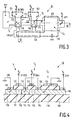
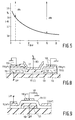
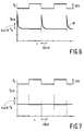
- This slow transient is removed in accordance with the present invention by injecting holes in the case of an n-channel TFT (or electrons in the case of a p channel TFT) into the body of the sampling transistor to neutralise the trapped charge when the transistor is being switched off. Particular characteristics are illustrated later by reference to the experimental results of Figures 5 to 7.
- An injector region and its connection in accordance with the present invention may be integrated with quite different types of TFT structure, both conventional types and new types.
Landscapes
- Engineering & Computer Science (AREA)
- Chemical & Material Sciences (AREA)
- Crystallography & Structural Chemistry (AREA)
- Physics & Mathematics (AREA)
- Computer Hardware Design (AREA)
- General Physics & Mathematics (AREA)
- Theoretical Computer Science (AREA)
- Thin Film Transistor (AREA)
- Liquid Crystal (AREA)
Applications Claiming Priority (2)
| Application Number | Priority Date | Filing Date | Title |
|---|---|---|---|
| GB939311129A GB9311129D0 (en) | 1993-05-28 | 1993-05-28 | Electronic devices with-film circuit elements forming a sampling circuit |
| GB9311129 | 1993-05-28 |
Publications (2)
| Publication Number | Publication Date |
|---|---|
| EP0629003A1 true EP0629003A1 (fr) | 1994-12-14 |
| EP0629003B1 EP0629003B1 (fr) | 1998-02-18 |
Family
ID=10736337
Family Applications (1)
| Application Number | Title | Priority Date | Filing Date |
|---|---|---|---|
| EP94201412A Expired - Lifetime EP0629003B1 (fr) | 1993-05-28 | 1994-05-18 | Dispositifs électroniques avec éléments de circuit à film mince formant un circuit d'échantillonnage |
Country Status (5)
| Country | Link |
|---|---|
| US (1) | US5684318A (fr) |
| EP (1) | EP0629003B1 (fr) |
| JP (1) | JP3987588B2 (fr) |
| DE (1) | DE69408556T2 (fr) |
| GB (1) | GB9311129D0 (fr) |
Cited By (10)
| Publication number | Priority date | Publication date | Assignee | Title |
|---|---|---|---|---|
| EP0816903A1 (fr) * | 1996-07-03 | 1998-01-07 | Hitachi, Ltd. | Dispositif à crystal liquide |
| WO1998027598A1 (fr) * | 1996-12-19 | 1998-06-25 | Honeywell Inc. | Dispositif mos avec connexion entre une partie corps et une partie gachette formee sur un substrat silicium-sur-isolant (ssi) |
| WO1999050911A3 (fr) * | 1998-03-28 | 1999-11-18 | Koninkl Philips Electronics Nv | Dispositifs electroniques composes de transistors en couche mince |
| WO2002007216A3 (fr) * | 2000-07-14 | 2002-05-10 | E Ink Corp | Fabrication d'elements de circuit electrique a l'aide de couches semi-conductrices depourvues de motifs |
| US7094654B2 (en) | 2001-03-23 | 2006-08-22 | Koninklijke Philips Electronics N.V. | Manufacture of electronic devices comprising thin-film transistors |
| US7256766B2 (en) | 1998-08-27 | 2007-08-14 | E Ink Corporation | Electrophoretic display comprising optical biasing element |
| US7405115B2 (en) | 2001-02-28 | 2008-07-29 | Semiconductor Energy Laboratory Co., Ltd. | Semiconductor device and manufacturing method thereof |
| US7414266B2 (en) | 2000-03-08 | 2008-08-19 | Semiconductor Energy Laboratory Co., Ltd. | Semiconductor device and manufacturing method thereof |
| EP1993089A3 (fr) * | 2007-05-18 | 2009-05-13 | Gigno Technology Co., Ltd. | Appareil de papier électronique et son circuit de commande et procédé de fabrication |
| US7687325B2 (en) | 2000-03-13 | 2010-03-30 | Semiconductor Energy Laboratory Co., Ltd. | Semiconductor device and manufacturing method thereof |
Families Citing this family (26)
| Publication number | Priority date | Publication date | Assignee | Title |
|---|---|---|---|---|
| US5808317A (en) * | 1996-07-24 | 1998-09-15 | International Business Machines Corporation | Split-gate, horizontally redundant, and self-aligned thin film transistors |
| US5973358A (en) * | 1997-07-01 | 1999-10-26 | Citizen Watch Co., Ltd. | SOI device having a channel with variable thickness |
| JP4027465B2 (ja) | 1997-07-01 | 2007-12-26 | 株式会社半導体エネルギー研究所 | アクティブマトリクス型表示装置およびその製造方法 |
| JP3838393B2 (ja) * | 1997-09-02 | 2006-10-25 | 株式会社半導体エネルギー研究所 | イメージセンサを内蔵した表示装置 |
| JP4271268B2 (ja) | 1997-09-20 | 2009-06-03 | 株式会社半導体エネルギー研究所 | イメージセンサおよびイメージセンサ一体型アクティブマトリクス型表示装置 |
| JP4044187B2 (ja) | 1997-10-20 | 2008-02-06 | 株式会社半導体エネルギー研究所 | アクティブマトリクス型表示装置およびその作製方法 |
| US6060749A (en) * | 1998-04-23 | 2000-05-09 | Texas Instruments - Acer Incorporated | Ultra-short channel elevated S/D MOSFETS formed on an ultra-thin SOI substrate |
| JPH11326954A (ja) | 1998-05-15 | 1999-11-26 | Semiconductor Energy Lab Co Ltd | 半導体装置 |
| US6734498B2 (en) * | 1998-10-02 | 2004-05-11 | Intel Corporation | Insulated channel field effect transistor with an electric field terminal region |
| US6452233B1 (en) * | 1999-03-23 | 2002-09-17 | Citizen Watch Co., Ltd. | SOI device having a leakage stopping layer |
| JP4118484B2 (ja) | 2000-03-06 | 2008-07-16 | 株式会社半導体エネルギー研究所 | 半導体装置の作製方法 |
| JP4700160B2 (ja) | 2000-03-13 | 2011-06-15 | 株式会社半導体エネルギー研究所 | 半導体装置 |
| JP4683688B2 (ja) | 2000-03-16 | 2011-05-18 | 株式会社半導体エネルギー研究所 | 液晶表示装置の作製方法 |
| JP4393662B2 (ja) | 2000-03-17 | 2010-01-06 | 株式会社半導体エネルギー研究所 | 液晶表示装置の作製方法 |
| JP4785229B2 (ja) | 2000-05-09 | 2011-10-05 | 株式会社半導体エネルギー研究所 | 半導体装置の作製方法 |
| JP4079655B2 (ja) * | 2001-02-28 | 2008-04-23 | 株式会社半導体エネルギー研究所 | 半導体装置およびその作製方法 |
| JP4593256B2 (ja) * | 2001-02-28 | 2010-12-08 | 株式会社半導体エネルギー研究所 | 半導体装置の作製方法 |
| US7071037B2 (en) | 2001-03-06 | 2006-07-04 | Semiconductor Energy Laboratory Co., Ltd. | Semiconductor device and manufacturing method thereof |
| GB0401579D0 (en) * | 2004-01-24 | 2004-02-25 | Koninkl Philips Electronics Nv | Transistor manufacture |
| JP2007134730A (ja) * | 2006-12-01 | 2007-05-31 | Semiconductor Energy Lab Co Ltd | 表示装置 |
| EP2077616A1 (fr) * | 2007-12-27 | 2009-07-08 | TPO Displays Corp. | Circuit et procédé de sortie de transistor |
| JP5888802B2 (ja) * | 2009-05-28 | 2016-03-22 | 株式会社半導体エネルギー研究所 | トランジスタを有する装置 |
| CN103730514B (zh) * | 2014-01-23 | 2019-07-19 | 苏州大学 | 薄膜晶体管 |
| CN105810749B (zh) * | 2014-12-31 | 2018-12-21 | 清华大学 | N型薄膜晶体管 |
| CN105810748B (zh) * | 2014-12-31 | 2018-12-21 | 清华大学 | N型薄膜晶体管 |
| US12211934B2 (en) | 2021-01-29 | 2025-01-28 | Taiwan Semiconductor Manufacturing Company, Ltd. | Semiconductor structure and method for manufacturing the same |
Citations (6)
| Publication number | Priority date | Publication date | Assignee | Title |
|---|---|---|---|---|
| FR2496342A1 (fr) * | 1980-12-12 | 1982-06-18 | Tokyo Shibaura Electric Co | Dispositif semi-conducteur du type metal-oxyde-semi-conducteur et son procede de fabrication |
| JPS6294986A (ja) * | 1985-10-21 | 1987-05-01 | Nec Corp | Mis型電界効果トランジスタとその駆動方法 |
| US4870399A (en) * | 1987-08-24 | 1989-09-26 | North American Philips Corporation | Apparatus for addressing active displays |
| EP0342925A2 (fr) * | 1988-05-17 | 1989-11-23 | Seiko Epson Corporation | Panneau d'affichage à matrice active |
| JPH0377922A (ja) * | 1989-08-21 | 1991-04-03 | Sharp Corp | 液晶表示装置 |
| JPH0377915A (ja) * | 1989-08-21 | 1991-04-03 | Sharp Corp | 液晶表示装置 |
Family Cites Families (5)
| Publication number | Priority date | Publication date | Assignee | Title |
|---|---|---|---|---|
| US3660732A (en) * | 1971-02-08 | 1972-05-02 | Signetics Corp | Semiconductor structure with dielectric and air isolation and method |
| DE3029539A1 (de) * | 1980-08-04 | 1982-03-11 | Deutsche Itt Industries Gmbh, 7800 Freiburg | Nichtfluechtige, programmierbare integrierte halbleiterspeicherzelle |
| DE69125886T2 (de) * | 1990-05-29 | 1997-11-20 | Semiconductor Energy Lab | Dünnfilmtransistoren |
| EP0497427B1 (fr) * | 1991-02-01 | 1996-04-10 | Koninklijke Philips Electronics N.V. | Dispositif semi-conducteur pour des applications à haute-tension et sa méthode de fabrication |
| JP2561413B2 (ja) * | 1993-02-23 | 1996-12-11 | 日産自動車株式会社 | 半導体装置 |
-
1993
- 1993-05-28 GB GB939311129A patent/GB9311129D0/en active Pending
-
1994
- 1994-05-18 DE DE69408556T patent/DE69408556T2/de not_active Expired - Fee Related
- 1994-05-18 EP EP94201412A patent/EP0629003B1/fr not_active Expired - Lifetime
- 1994-05-26 JP JP11284494A patent/JP3987588B2/ja not_active Expired - Lifetime
-
1996
- 1996-04-25 US US08/639,277 patent/US5684318A/en not_active Expired - Fee Related
Patent Citations (6)
| Publication number | Priority date | Publication date | Assignee | Title |
|---|---|---|---|---|
| FR2496342A1 (fr) * | 1980-12-12 | 1982-06-18 | Tokyo Shibaura Electric Co | Dispositif semi-conducteur du type metal-oxyde-semi-conducteur et son procede de fabrication |
| JPS6294986A (ja) * | 1985-10-21 | 1987-05-01 | Nec Corp | Mis型電界効果トランジスタとその駆動方法 |
| US4870399A (en) * | 1987-08-24 | 1989-09-26 | North American Philips Corporation | Apparatus for addressing active displays |
| EP0342925A2 (fr) * | 1988-05-17 | 1989-11-23 | Seiko Epson Corporation | Panneau d'affichage à matrice active |
| JPH0377922A (ja) * | 1989-08-21 | 1991-04-03 | Sharp Corp | 液晶表示装置 |
| JPH0377915A (ja) * | 1989-08-21 | 1991-04-03 | Sharp Corp | 液晶表示装置 |
Non-Patent Citations (3)
| Title |
|---|
| D RIGAUD ET AL.: "INFLUENCE OF THE BULK ELECTRODE ON THE CHARACTERISITCS AND THE CHANNEL NOISE OF SOS-MOS TRANSISTORS", REVUE DE PHYSIQUE APPLIQUÉE, vol. 15, no. 5, May 1980 (1980-05-01), PARIS, FRANCE, pages 937 - 940 * |
| PATENT ABSTRACTS OF JAPAN vol. 11, no. 304 (E - 545) 3 October 1987 (1987-10-03) * |
| PATENT ABSTRACTS OF JAPAN vol. 15, no. 245 (P - 1218) 24 June 1991 (1991-06-24) * |
Cited By (17)
| Publication number | Priority date | Publication date | Assignee | Title |
|---|---|---|---|---|
| US6104040A (en) * | 1996-03-07 | 2000-08-15 | Hitachi, Ltd. | Liquid crystal display having a transistor with doped region in an active semiconductor layer |
| KR100546905B1 (ko) * | 1996-07-03 | 2006-08-22 | 가부시끼가이샤 히다치 세이사꾸쇼 | 액정표시장치 |
| US6812489B2 (en) | 1996-07-03 | 2004-11-02 | Hitachi, Ltd. | Liquid crystal display |
| EP0816903A1 (fr) * | 1996-07-03 | 1998-01-07 | Hitachi, Ltd. | Dispositif à crystal liquide |
| WO1998027598A1 (fr) * | 1996-12-19 | 1998-06-25 | Honeywell Inc. | Dispositif mos avec connexion entre une partie corps et une partie gachette formee sur un substrat silicium-sur-isolant (ssi) |
| US6046479A (en) * | 1998-03-28 | 2000-04-04 | U.S. Philips Corporation | Electronic devices comprising thin-film transistors |
| WO1999050911A3 (fr) * | 1998-03-28 | 1999-11-18 | Koninkl Philips Electronics Nv | Dispositifs electroniques composes de transistors en couche mince |
| US7256766B2 (en) | 1998-08-27 | 2007-08-14 | E Ink Corporation | Electrophoretic display comprising optical biasing element |
| US7414266B2 (en) | 2000-03-08 | 2008-08-19 | Semiconductor Energy Laboratory Co., Ltd. | Semiconductor device and manufacturing method thereof |
| US9786687B2 (en) | 2000-03-08 | 2017-10-10 | Semiconductor Energy Laboratory Co., Ltd. | Semiconductor device and manufacturing method thereof |
| US7687325B2 (en) | 2000-03-13 | 2010-03-30 | Semiconductor Energy Laboratory Co., Ltd. | Semiconductor device and manufacturing method thereof |
| WO2002007216A3 (fr) * | 2000-07-14 | 2002-05-10 | E Ink Corp | Fabrication d'elements de circuit electrique a l'aide de couches semi-conductrices depourvues de motifs |
| US7405115B2 (en) | 2001-02-28 | 2008-07-29 | Semiconductor Energy Laboratory Co., Ltd. | Semiconductor device and manufacturing method thereof |
| US8053339B2 (en) | 2001-02-28 | 2011-11-08 | Semiconductor Energy Laboratory Co., Ltd. | Semiconductor device and manufacturing method thereof |
| US8735889B2 (en) | 2001-02-28 | 2014-05-27 | Semiconductor Energy Laboratory Co., Ltd. | Semiconductor device and manufacturing method thereof |
| US7094654B2 (en) | 2001-03-23 | 2006-08-22 | Koninklijke Philips Electronics N.V. | Manufacture of electronic devices comprising thin-film transistors |
| EP1993089A3 (fr) * | 2007-05-18 | 2009-05-13 | Gigno Technology Co., Ltd. | Appareil de papier électronique et son circuit de commande et procédé de fabrication |
Also Published As
| Publication number | Publication date |
|---|---|
| JP3987588B2 (ja) | 2007-10-10 |
| EP0629003B1 (fr) | 1998-02-18 |
| DE69408556D1 (de) | 1998-03-26 |
| DE69408556T2 (de) | 1998-08-13 |
| GB9311129D0 (en) | 1993-07-14 |
| JPH06338615A (ja) | 1994-12-06 |
| US5684318A (en) | 1997-11-04 |
Similar Documents
| Publication | Publication Date | Title |
|---|---|---|
| EP0629003B1 (fr) | Dispositifs électroniques avec éléments de circuit à film mince formant un circuit d'échantillonnage | |
| US5552615A (en) | Active matrix assembly with double layer metallization over drain contact region | |
| US6259117B1 (en) | Active matrix display having storage capacitor associated with each pixel transistor | |
| US5365079A (en) | Thin film transistor and display device including same | |
| US6046479A (en) | Electronic devices comprising thin-film transistors | |
| EP0742944A1 (fr) | Memoire a semi-conducteur dotee d'un transistor a memoire remanente | |
| US5703382A (en) | Array having multiple channel structures with continuously doped interchannel regions | |
| EP0342925A2 (fr) | Panneau d'affichage à matrice active | |
| US6404271B2 (en) | Charge pump circuit | |
| KR100727714B1 (ko) | 반도체 장치 및 화상 표시 장치 | |
| US5828430A (en) | Active matrix type liquid crystal display apparatus having optical shield layer capable of suppressing display distortion | |
| EP0280370B1 (fr) | Transistors à couche mince, dispositifs d'affichage les comprenant et leurs méthodes de fabrication | |
| US20020167051A1 (en) | Electronic device including a thin film transistor | |
| JP2898509B2 (ja) | アクティブマトリックス基板及びその製造方法 | |
| US4365262A (en) | Semiconductor image sensor | |
| JP2668317B2 (ja) | アクティブマトリクスパネル | |
| Wu et al. | A novel depletion-gate amorphous silicon thin-film transistor | |
| JPH06138492A (ja) | 液晶表示装置 | |
| JPH0722201B2 (ja) | 液晶表示装置の製造方法 |
Legal Events
| Date | Code | Title | Description |
|---|---|---|---|
| PUAI | Public reference made under article 153(3) epc to a published international application that has entered the european phase |
Free format text: ORIGINAL CODE: 0009012 |
|
| AK | Designated contracting states |
Kind code of ref document: A1 Designated state(s): DE FR GB IT NL |
|
| 17P | Request for examination filed |
Effective date: 19950614 |
|
| GRAG | Despatch of communication of intention to grant |
Free format text: ORIGINAL CODE: EPIDOS AGRA |
|
| 17Q | First examination report despatched |
Effective date: 19970421 |
|
| GRAG | Despatch of communication of intention to grant |
Free format text: ORIGINAL CODE: EPIDOS AGRA |
|
| GRAG | Despatch of communication of intention to grant |
Free format text: ORIGINAL CODE: EPIDOS AGRA |
|
| GRAH | Despatch of communication of intention to grant a patent |
Free format text: ORIGINAL CODE: EPIDOS IGRA |
|
| GRAH | Despatch of communication of intention to grant a patent |
Free format text: ORIGINAL CODE: EPIDOS IGRA |
|
| GRAA | (expected) grant |
Free format text: ORIGINAL CODE: 0009210 |
|
| AK | Designated contracting states |
Kind code of ref document: B1 Designated state(s): DE FR GB IT NL |
|
| PG25 | Lapsed in a contracting state [announced via postgrant information from national office to epo] |
Ref country code: NL Free format text: LAPSE BECAUSE OF FAILURE TO SUBMIT A TRANSLATION OF THE DESCRIPTION OR TO PAY THE FEE WITHIN THE PRESCRIBED TIME-LIMIT Effective date: 19980218 Ref country code: IT Free format text: LAPSE BECAUSE OF FAILURE TO SUBMIT A TRANSLATION OF THE DESCRIPTION OR TO PAY THE FEE WITHIN THE PRE;WARNING: LAPSES OF ITALIAN PATENTS WITH EFFECTIVE DATE BEFORE 2007 MAY HAVE OCCURRED AT ANY TIME BEFORE 2007. THE CORRECT EFFECTIVE DATE MAY BE DIFFERENT FROM THE ONE RECORDED.SCRIBED TIME-LIMIT Effective date: 19980218 |
|
| REF | Corresponds to: |
Ref document number: 69408556 Country of ref document: DE Date of ref document: 19980326 |
|
| ET | Fr: translation filed | ||
| NLV1 | Nl: lapsed or annulled due to failure to fulfill the requirements of art. 29p and 29m of the patents act | ||
| REG | Reference to a national code |
Ref country code: FR Ref legal event code: CD |
|
| PLBE | No opposition filed within time limit |
Free format text: ORIGINAL CODE: 0009261 |
|
| STAA | Information on the status of an ep patent application or granted ep patent |
Free format text: STATUS: NO OPPOSITION FILED WITHIN TIME LIMIT |
|
| 26N | No opposition filed | ||
| REG | Reference to a national code |
Ref country code: GB Ref legal event code: IF02 |
|
| REG | Reference to a national code |
Ref country code: FR Ref legal event code: D6 |
|
| REG | Reference to a national code |
Ref country code: GB Ref legal event code: 746 Effective date: 20021107 |
|
| PGFP | Annual fee paid to national office [announced via postgrant information from national office to epo] |
Ref country code: DE Payment date: 20080716 Year of fee payment: 15 |
|
| PGFP | Annual fee paid to national office [announced via postgrant information from national office to epo] |
Ref country code: FR Payment date: 20080528 Year of fee payment: 15 |
|
| PGFP | Annual fee paid to national office [announced via postgrant information from national office to epo] |
Ref country code: GB Payment date: 20080616 Year of fee payment: 15 |
|
| GBPC | Gb: european patent ceased through non-payment of renewal fee |
Effective date: 20090518 |
|
| REG | Reference to a national code |
Ref country code: FR Ref legal event code: ST Effective date: 20100129 |
|
| PG25 | Lapsed in a contracting state [announced via postgrant information from national office to epo] |
Ref country code: FR Free format text: LAPSE BECAUSE OF NON-PAYMENT OF DUE FEES Effective date: 20090602 |
|
| PG25 | Lapsed in a contracting state [announced via postgrant information from national office to epo] |
Ref country code: GB Free format text: LAPSE BECAUSE OF NON-PAYMENT OF DUE FEES Effective date: 20090518 |
|
| PG25 | Lapsed in a contracting state [announced via postgrant information from national office to epo] |
Ref country code: DE Free format text: LAPSE BECAUSE OF NON-PAYMENT OF DUE FEES Effective date: 20091201 |