EP0629006A1 - Supraleitender Schalter und Anwendung als Speisung einer supraleitenden Spule - Google Patents
Supraleitender Schalter und Anwendung als Speisung einer supraleitenden Spule Download PDFInfo
- Publication number
- EP0629006A1 EP0629006A1 EP94400947A EP94400947A EP0629006A1 EP 0629006 A1 EP0629006 A1 EP 0629006A1 EP 94400947 A EP94400947 A EP 94400947A EP 94400947 A EP94400947 A EP 94400947A EP 0629006 A1 EP0629006 A1 EP 0629006A1
- Authority
- EP
- European Patent Office
- Prior art keywords
- superconductive
- switch
- cable
- coil
- superconducting
- Prior art date
- Legal status (The legal status is an assumption and is not a legal conclusion. Google has not performed a legal analysis and makes no representation as to the accuracy of the status listed.)
- Granted
Links
- 239000004020 conductor Substances 0.000 claims abstract description 28
- 239000012212 insulator Substances 0.000 claims abstract description 8
- 239000002826 coolant Substances 0.000 claims abstract description 6
- 239000000615 nonconductor Substances 0.000 claims abstract description 6
- 238000004804 winding Methods 0.000 claims description 20
- 239000003990 capacitor Substances 0.000 claims description 10
- 230000007704 transition Effects 0.000 claims description 4
- 238000010438 heat treatment Methods 0.000 description 7
- 238000009413 insulation Methods 0.000 description 6
- 229910000570 Cupronickel Inorganic materials 0.000 description 4
- 238000010586 diagram Methods 0.000 description 4
- 230000000694 effects Effects 0.000 description 3
- 229910052734 helium Inorganic materials 0.000 description 3
- 239000001307 helium Substances 0.000 description 3
- SWQJXJOGLNCZEY-UHFFFAOYSA-N helium atom Chemical compound [He] SWQJXJOGLNCZEY-UHFFFAOYSA-N 0.000 description 3
- 238000011084 recovery Methods 0.000 description 3
- 238000001816 cooling Methods 0.000 description 2
- 239000010949 copper Substances 0.000 description 2
- PMHQVHHXPFUNSP-UHFFFAOYSA-M copper(1+);methylsulfanylmethane;bromide Chemical compound Br[Cu].CSC PMHQVHHXPFUNSP-UHFFFAOYSA-M 0.000 description 2
- 238000010292 electrical insulation Methods 0.000 description 2
- 238000002955 isolation Methods 0.000 description 2
- 239000007788 liquid Substances 0.000 description 2
- 239000000463 material Substances 0.000 description 2
- RYGMFSIKBFXOCR-UHFFFAOYSA-N Copper Chemical compound [Cu] RYGMFSIKBFXOCR-UHFFFAOYSA-N 0.000 description 1
- 229910000896 Manganin Inorganic materials 0.000 description 1
- 229910052802 copper Inorganic materials 0.000 description 1
- 230000007423 decrease Effects 0.000 description 1
- 238000004534 enameling Methods 0.000 description 1
- 230000005291 magnetic effect Effects 0.000 description 1
- 239000011159 matrix material Substances 0.000 description 1
- RJSRQTFBFAJJIL-UHFFFAOYSA-N niobium titanium Chemical compound [Ti].[Nb] RJSRQTFBFAJJIL-UHFFFAOYSA-N 0.000 description 1
- 210000000056 organ Anatomy 0.000 description 1
- 239000011347 resin Substances 0.000 description 1
- 229920005989 resin Polymers 0.000 description 1
- 239000002887 superconductor Substances 0.000 description 1
- 239000002470 thermal conductor Substances 0.000 description 1
- 238000003466 welding Methods 0.000 description 1
Images



Classifications
-
- H—ELECTRICITY
- H10—SEMICONDUCTOR DEVICES; ELECTRIC SOLID-STATE DEVICES NOT OTHERWISE PROVIDED FOR
- H10N—ELECTRIC SOLID-STATE DEVICES NOT OTHERWISE PROVIDED FOR
- H10N60/00—Superconducting devices
- H10N60/30—Devices switchable between superconducting and normal states
- H10N60/35—Cryotrons
- H10N60/355—Power cryotrons
Definitions
- the present invention relates to a superconductive switch.
- a full-wave rectifier device comprising a primary winding and two secondary windings arranged in parallel and wound in opposite directions from each other and connected to a superconducting coil to charge it.
- the secondary windings each consist of 1610 superconducting wires connected in parallel, organized into 230 strips of 7 wires.
- the strips are brought together in groups of 10, thus making 23 groups put in parallel with 7 X 10 wires in parallel, thus constituting a single superconductive conductor.
- this conductor is wound on the external surface of a cylinder, helically, on 11 è 23 in turn and for the other, in reverse, on 12 è 23 of turn on the internal surface of the cylinder inside which is the primary winding.
- Each of the secondary windings is equipped with two heating elements, over a small width, 5 mm, of the conductor forming this winding: one on each face of the conductor.
- a heating element consists of a plurality of turns of a manganin wire.
- These heating elements serve to alternate the two superconductive conductors constituting the two secondary windings supplying the superconductive coil to be charged.
- the invention aims to overcome these drawbacks and relates to a superconductive switch composed of a portion of cable comprising a resistive central strand, non-superconductive around which are stranded a plurality of superconductive strands, or superconductive conductors, separate of said central strand by an electrical insulator, the assembly being isolated from the outside, cooling medium, by a thermal insulator, at each end of said cable portion, said central strand being electrically connected to said superconductive strands or to superconductive conductors, characterized in that, at a point along the length of said cable portion, a length portion of said resistive central strand exits from said cable and is coupled to a control device located outside of said cooling medium, said control device consisting of means to inject an electric current into the circuit formed by the central strand resi stif connected at its ends to the superconductive strands or to the superconductive conductors.
- said length portion of said resistive central strand leaving said cable is cut, thus forming two ends which are connected to said control device which comprises a capacitor in series with a discharge switch, a voltage source being connected to the terminals of said capacitor via a load resistor and a load switch.
- a subject of the invention is also a charger for a superconductive coil comprising, in an environment at ambient temperature, an alternating voltage source connected to a full-wave rectifier circuit supplying the superconductive coil, the rectifier and the coil being located in a refrigerating medium.
- the rectifier circuit comprising a transformer comprising a primary winding and a secondary winding in two parts, each part being connected in parallel to the coil and supplying it alternately by means of a control means ensuring half-alternation in two the transition from the superconductive state to the normal state of the connection of the considered part of said secondary winding with the coil, characterized in that said control means comprises a superconducting switch as defined above.
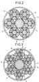
- Figure 1, 2 and 3 show in section, three examples of cables that can be used to make a superconducting switch according to the invention.
- FIG. 4 shows a superconductive switch according to the invention.
- FIG. 5 is an electrical diagram symbolizing a superconductive switch according to the invention inserted in a superconductive line and showing a particular control device.
- Figure 6 is an electrical diagram similar to Figure 5 showing another arrangement for the control device.
- FIG. 7 is an electrical diagram representing a coil charger with superconductive switches controlled in accordance with FIG. 5.
- FIG. 1 we can see the cross section of a cable as it can be used to make a superconductive switch according to the invention and represented in FIGS. 4, 5 and 6.
- the cable shown is composed of six superconductive strands 1, each consisting of filaments of titanium Niobium (NbTi) embedded in a Cupro Nickel (CuNi) matrix, stranded around a central resistive strand, not superconductive.
- This central strand can be made either of CuNi, or of CuNi containing copper (Cu) filaments, it is separated from the six superconductive strands 1 by an electrical insulator 3.
- This insulator 3 is preferably a good thermal conductor in order to allow the heat given off in the central strand 2 by the Joule effect of rapidly diffusing into the superconductive strands 1.
- a material that meets these conditions well: electrical insulation and good thermal conduction is Aluminum Nitride or any similar material.
- the insulator 3 is for example made of a resin loaded with aluminum nitride.
- the entire cable is insulated by a thermal insulator 4.
- the length portion of such a cable, used as a superconductive switch is located, in operation, in a cooling medium such as liquid helium at 4, 2 ° K.
- This thermal insulation 4 must be sufficient to limit the power necessary for heating the superconducting strands 1 by the power dissipated in the central strand 2 but must also be minimized so as to allow recovery of the superconductive state (by cooling the superconductive strands). in times compatible with high frequency operations such as 50 Hz.
- Figure 2 shows another example of a cable that can be used to make a superconducting switch.
- the cable consists of six superconductive conductors 5 assembled in a strand around a central resistive strand 2 non-superconductive and separated from the latter by an electrical insulator 3, the assembly being insulated by a thermal insulator 4.
- An example of a conductor superconductor as 5 is described in patent document FR-A-2674671.
- FIG. 3 shows yet another example of cable which can be used to make a superconductive switch according to the invention.
- the cable consists, as in FIG. 2, of six superconductive conductors 6 assembled in a strand around a central resistive strand 2, non-superconductive, and separated from the latter by an electrical insulator 3, the assembly being insulated by an insulator thermal 4.
- superconductive strands 7 and central strand 8 have a circular section.
- FIG. 4 represents a superconductive switch according to the invention:
- Such a switch consists of a length portion of a cable 30 of the type as described with reference to FIGS. 1, 2 or 3.
- the superconductive strands 1, in the case of the cable of FIG. 1, or the superconductive conductors 5 or 6 in the case of the cable of FIGS. 2 or 3, are connected in parallel to the central strand resistive 2.
- the resistive central strand 2 is separated from the superconductive strands 1, or the superconductive conductors 5 or 6, and exits outside the cable 30 and, after crossing the refrigerating medium at 4.2 ° K where the cable is located, is coupled to a control device 12 located in the ambient environment around 300 ° K.
- the role of this control device is to inject an electric current into the circuit formed by the central resistive strand 2 in parallel with the superconductive strands 1 (or the superconductive conductors 5 or 6).
- FIG. 5 is an electrical diagram which represents the switch of FIG. 4 inserted in a current line 13 and in which a particular control device 12 is shown.
- the switch is represented by a parallel circuit comprising the superconductive strands 1 (or the superconductive conductors 5, 6) represented by a single wire and the central resistive strand 2 represented by a wire comprising a resistor R.
- the resistive strand 2 is cut and its ends 14, 15 are connected to the control device 12 located at an ambient temperature of 300 ° K.
- This device comprises a capacitor 16 arranged in series with a discharge switch 17. At the terminals of the capacitor 16 is located a voltage source 18 in series with a load resistor 19 and a charge switch 20.
- the capacitor 16 In the first operating phase, the capacitor 16 is charged by closing the switch 20, the switch 17 being open. The capacitor is then charged through the resistor 19 to the charge voltage of the source 18 thus storing energy. Switch 20 is then open and the circuit is in the waiting phase.
- the switch 17 When ordering for circuit switching or "closing the switch", the switch 17 is closed, the capacitor 16 then discharges into the circuit formed by the resistive central strand 2 and the superconductive strands 1 (or superconductive conductors 5 or 6).
- the passage of the current in the resistive strand 2 assimilated to the resistance R, gives off heat by Joule effect which diffuses in the superconductive strands 1, (5 or 6) causing their transition to the normal non-superconductive state.
- the switches 17 and 20 can, of course, be switches controlled by thyristors, or by transistors, allowing the device to operate at the desired frequency.
- the covering in the superconductive state of the strands 1 is done by itself by cooling these strands by the refrigerating medium to 4.2 ° K in which the circuit is located, as soon as the discharge current of the capacitor 17 has ceased.
- FIG. 6 shows another control device 12 which generates, by appropriate control 21 of the primary of a transformer 22, a voltage slot at the terminals of the secondary of said transformer 22 connected to the ends 14 and 15.
- FIG. 7 shows an application of the switch device, it is a charger for a superconductive coil 23.
- the direct charge of a superconducting coil under large currents generates cryogenic losses which can become very large with strong currents through the current leads.
- the role of the current leads is to convey the current, from the source, which is at ambient temperature of approximately 300 ° K, to the superconductive coil which is at the temperature of liquid helium: 4.2 ° K.
- This coil charger comprises an alternating voltage source 24, located at ambient temperature of approximately 300 ° K, connected to a full-wave rectifier circuit comprising a transformer whose primary winding 25 has a large number of turns N1 and whose secondary is in two parts 26 and 26A which have a number of turns N2 much lower than that of the primary winding.
- Each secondary winding 26 and 26A is connected in parallel to the coil 23 by means of a control means, consisting of a switch and its control device conforming to that of FIG. 5, ensuring half of two alternations , the transition from the superconductive state to the normal state of the superconductive strands 1 (or of the superconductive conductors 5 or 6).
- the references of the control means located on the side of the secondary winding 26A have been assigned an index A.
- one alternation in two is the coil 26 which supplies the coil 23, the corresponding "switch” being closed and the other, that with the indices A, open, and the other alternation, it is the coil 26A which supplies the coil 23, the corresponding "switch” being closed and the other, the one without indices, open.
- the switches 17, 20, 17A and 20A are controlled electronic switches, for example with thyristors.
- the primary current in the winding 25 is much lower than that of the secondary windings 26 and 26A which is equal to the load current of the coil 23.
- the coil is supplied either by the coil 26 or by the coil 26A and the current in the coil increases by a certain value. In fact, at each alternation, a certain amount of energy is transferred from the primary circuit to the coil 23.
- a superconductive switch 27 is closed bypassing the two ends of the coil which thus stores a certain energy.
- the device described in the present invention allows operation at 50 Hz and is therefore particularly advantageous in the case of an application to a coil charger.
- a switch such as that shown in FIG. 5 with its control, must have an opening time (passage of the strands 1, or of the conductors 5 or 6, from the superconductive state to the normal state) of the order 1 ms and a closing time (recovery of the superconducting state) of 2 to 3 ms.
Landscapes
- Containers, Films, And Cooling For Superconductive Devices (AREA)
- Superconductors And Manufacturing Methods Therefor (AREA)
- Resistance Heating (AREA)
- Charge And Discharge Circuits For Batteries Or The Like (AREA)
Applications Claiming Priority (2)
| Application Number | Priority Date | Filing Date | Title |
|---|---|---|---|
| FR9305367 | 1993-05-05 | ||
| FR9305367A FR2704980B1 (fr) | 1993-05-05 | 1993-05-05 | Interrupteur supraconducteur et application à un chargeur de bobine supraconductrice. |
Publications (2)
| Publication Number | Publication Date |
|---|---|
| EP0629006A1 true EP0629006A1 (de) | 1994-12-14 |
| EP0629006B1 EP0629006B1 (de) | 1997-04-16 |
Family
ID=9446787
Family Applications (1)
| Application Number | Title | Priority Date | Filing Date |
|---|---|---|---|
| EP94400947A Expired - Lifetime EP0629006B1 (de) | 1993-05-05 | 1994-05-02 | Supraleitender Schalter und Anwendung als Speisung einer supraleitenden Spule |
Country Status (7)
| Country | Link |
|---|---|
| US (1) | US5545932A (de) |
| EP (1) | EP0629006B1 (de) |
| AT (1) | ATE151918T1 (de) |
| DE (1) | DE69402610T2 (de) |
| DK (1) | DK0629006T3 (de) |
| ES (1) | ES2100025T3 (de) |
| FR (1) | FR2704980B1 (de) |
Families Citing this family (10)
| Publication number | Priority date | Publication date | Assignee | Title |
|---|---|---|---|---|
| US6110606A (en) | 1996-08-30 | 2000-08-29 | American Superconductor Corporation | Cryogen protected superconducting ceramic tape |
| US6444917B1 (en) | 1999-07-23 | 2002-09-03 | American Superconductor Corporation | Encapsulated ceramic superconductors |
| US7168165B2 (en) * | 2005-03-07 | 2007-01-30 | Medtronic, Inc. | Fabrication of electrical medical leads employing multi-filar wire conductors |
| US8049470B2 (en) * | 2007-06-11 | 2011-11-01 | Smartsynch, Inc. | Apparatus and method for charging super capacitors at limited voltage and/or current values irrespective of temperature |
| WO2014058871A1 (en) * | 2012-10-12 | 2014-04-17 | Brookhaven Science Associates/Brookhaven National Laboratory | Fast superconducting switch for superconducting power devices |
| GB2525218B (en) * | 2014-04-16 | 2016-08-03 | Siemens Healthcare Ltd | High di/dt superconductive switch |
| GB2544052B (en) * | 2015-11-03 | 2020-01-15 | Rolls Royce Plc | Cooling system for electrical equipment |
| US20180122544A1 (en) * | 2016-11-03 | 2018-05-03 | Mevion Medical Systems, Inc. | Superconducting coil configuration |
| US10971291B2 (en) | 2017-06-30 | 2021-04-06 | The Boeing Company | System and method for operating a bulk superconductor device |
| US11070123B2 (en) | 2017-07-07 | 2021-07-20 | The Boeing Compan | Energy storage and energy storage device |
Citations (6)
| Publication number | Priority date | Publication date | Assignee | Title |
|---|---|---|---|---|
| US3444307A (en) * | 1966-03-23 | 1969-05-13 | Siemens Ag | Cooling system for superconductive or cryogenic structures |
| JPS62214680A (ja) * | 1986-03-14 | 1987-09-21 | Hitachi Cable Ltd | 熱式永久電流スイツチ用超電導々体 |
| JPH01136317A (ja) * | 1987-11-24 | 1989-05-29 | Hitachi Cable Ltd | 永久電流スイッチ用超電導線およびその製造方法 |
| US4906861A (en) * | 1988-09-30 | 1990-03-06 | Cryomagnetics, Inc. | Superconducting current reversing switch |
| FR2674671A1 (fr) * | 1991-03-28 | 1992-10-02 | Alsthom Gec | Conducteur supraconducteur possedant une protection amelioree contre les transitions partielles. |
| WO1994003955A1 (en) * | 1992-07-31 | 1994-02-17 | Arch Development Corporation | High temperature superconducting fault current limiter |
Family Cites Families (4)
| Publication number | Priority date | Publication date | Assignee | Title |
|---|---|---|---|---|
| US3848162A (en) * | 1972-07-11 | 1974-11-12 | President Of The Agency Of Ind | Method and apparatus for charging a superconductive coil |
| NL8501762A (nl) * | 1985-06-19 | 1987-01-16 | Holec Syst & Componenten | Supergeleidende gelijkrichter voor het omzetten van een relatief lage wisselstroom in een relatief hoge gelijkstroom. |
| US5227669A (en) * | 1991-03-19 | 1993-07-13 | American Electronic Laboratories, Inc. | Superconducting non-linear device |
| ATE150204T1 (de) * | 1992-11-05 | 1997-03-15 | Gec Alsthom T & D Sa | Supraleitende wicklung, insbesondere für strombegrenzer und strombegrenzer mit einer solchen wicklung |
-
1993
- 1993-05-05 FR FR9305367A patent/FR2704980B1/fr not_active Expired - Fee Related
-
1994
- 1994-04-14 US US08/227,335 patent/US5545932A/en not_active Expired - Fee Related
- 1994-05-02 DK DK94400947.1T patent/DK0629006T3/da active
- 1994-05-02 ES ES94400947T patent/ES2100025T3/es not_active Expired - Lifetime
- 1994-05-02 DE DE69402610T patent/DE69402610T2/de not_active Expired - Fee Related
- 1994-05-02 EP EP94400947A patent/EP0629006B1/de not_active Expired - Lifetime
- 1994-05-02 AT AT94400947T patent/ATE151918T1/de not_active IP Right Cessation
Patent Citations (6)
| Publication number | Priority date | Publication date | Assignee | Title |
|---|---|---|---|---|
| US3444307A (en) * | 1966-03-23 | 1969-05-13 | Siemens Ag | Cooling system for superconductive or cryogenic structures |
| JPS62214680A (ja) * | 1986-03-14 | 1987-09-21 | Hitachi Cable Ltd | 熱式永久電流スイツチ用超電導々体 |
| JPH01136317A (ja) * | 1987-11-24 | 1989-05-29 | Hitachi Cable Ltd | 永久電流スイッチ用超電導線およびその製造方法 |
| US4906861A (en) * | 1988-09-30 | 1990-03-06 | Cryomagnetics, Inc. | Superconducting current reversing switch |
| FR2674671A1 (fr) * | 1991-03-28 | 1992-10-02 | Alsthom Gec | Conducteur supraconducteur possedant une protection amelioree contre les transitions partielles. |
| WO1994003955A1 (en) * | 1992-07-31 | 1994-02-17 | Arch Development Corporation | High temperature superconducting fault current limiter |
Non-Patent Citations (3)
| Title |
|---|
| G. B. J. MULDER ET AL, IEEE TRANSACTIONS ON MAGNETICS., vol. 27, no. 2, March 1991 (1991-03-01), NEW YORK US, pages 2333 - 2336 * |
| PATENT ABSTRACTS OF JAPAN vol. 012, no. 072 (E - 588) 5 March 1988 (1988-03-05) * |
| PATENT ABSTRACTS OF JAPAN vol. 013, no. 386 (E - 812) 25 August 1989 (1989-08-25) * |
Also Published As
| Publication number | Publication date |
|---|---|
| US5545932A (en) | 1996-08-13 |
| DE69402610D1 (de) | 1997-05-22 |
| EP0629006B1 (de) | 1997-04-16 |
| DK0629006T3 (de) | 1997-05-26 |
| FR2704980B1 (fr) | 1995-06-09 |
| ES2100025T3 (es) | 1997-06-01 |
| DE69402610T2 (de) | 1997-07-17 |
| ATE151918T1 (de) | 1997-05-15 |
| FR2704980A1 (fr) | 1994-11-10 |
Similar Documents
| Publication | Publication Date | Title |
|---|---|---|
| FR2677503A1 (fr) | Limiteur de courant. | |
| EP0629006B1 (de) | Supraleitender Schalter und Anwendung als Speisung einer supraleitenden Spule | |
| EP2146395B1 (de) | Anschlussmuffe eines Supraleiterkabels und Abschluss des Anschlusses mit Hilfe dieser Muffe | |
| FR2629956A1 (fr) | Limiteur de courant | |
| EP2110887B1 (de) | Verbindungsanordnung von zwei Supraleitungskabeln | |
| CA2468216C (en) | Phase split structure of multiphase superconducting cable | |
| EP2523291A1 (de) | Abzweigelement für eine Supraleiterkabeleinheit | |
| EP0610131B1 (de) | Verbindungsdurchführung für supraleitende Spule | |
| US4169964A (en) | Electrical superconductor | |
| EP2852001A1 (de) | Verbindungsvorrichtung für supraleitende Kabel | |
| FR2555799A1 (fr) | Cable electrique, notamment pour usage aerospatial, a caracteristiques electriques ameliorees | |
| EP0440127B1 (de) | Gegen partielle Übergänge geschützter Supraleiter | |
| FR2548838A1 (fr) | Procede pour realiser une connexion entre fils supraconducteurs et connexion obtenue par ce procede | |
| EP0203952B1 (de) | Eisenkernloser elektromagnet | |
| EP0794545B1 (de) | Vakuumschalter oder Lastschalter | |
| CH621653A5 (de) | ||
| FR2621734A1 (fr) | Disjoncteur a haute tension a courant continu | |
| IL26689A (en) | Device and method for releasing electrical energy | |
| JPH08321416A (ja) | 超電導装置用電流リード | |
| FR2958807A1 (fr) | Dispositif de connexion de deux cables supraconducteurs | |
| EP0667628B1 (de) | Supraleitende Spule mit allgemeinen Übergang | |
| FR2637728A1 (fr) | Amenee de courant cryogenique a faibles pertes | |
| EP0803881B1 (de) | Hochspannungsstrombegrenzer auf Polymerbasis | |
| EP0505975B1 (de) | Supraleiter mit verbessertem Schutz gegen partielle Übergänge | |
| BE353147A (fr) | Installation à rayons chi |
Legal Events
| Date | Code | Title | Description |
|---|---|---|---|
| PUAI | Public reference made under article 153(3) epc to a published international application that has entered the european phase |
Free format text: ORIGINAL CODE: 0009012 |
|
| AK | Designated contracting states |
Kind code of ref document: A1 Designated state(s): AT BE CH DE DK ES FR GB IE IT LI LU NL PT SE |
|
| 17P | Request for examination filed |
Effective date: 19950515 |
|
| GRAG | Despatch of communication of intention to grant |
Free format text: ORIGINAL CODE: EPIDOS AGRA |
|
| 17Q | First examination report despatched |
Effective date: 19960808 |
|
| GRAH | Despatch of communication of intention to grant a patent |
Free format text: ORIGINAL CODE: EPIDOS IGRA |
|
| GRAH | Despatch of communication of intention to grant a patent |
Free format text: ORIGINAL CODE: EPIDOS IGRA |
|
| RHK1 | Main classification (correction) |
Ipc: H01L 39/20 |
|
| GRAA | (expected) grant |
Free format text: ORIGINAL CODE: 0009210 |
|
| PGFP | Annual fee paid to national office [announced via postgrant information from national office to epo] |
Ref country code: FR Payment date: 19970411 Year of fee payment: 4 |
|
| AK | Designated contracting states |
Kind code of ref document: B1 Designated state(s): AT BE CH DE DK ES FR GB IE IT LI LU NL PT SE |
|
| REF | Corresponds to: |
Ref document number: 151918 Country of ref document: AT Date of ref document: 19970515 Kind code of ref document: T |
|
| PGFP | Annual fee paid to national office [announced via postgrant information from national office to epo] |
Ref country code: IE Payment date: 19970417 Year of fee payment: 4 Ref country code: BE Payment date: 19970417 Year of fee payment: 4 |
|
| ITF | It: translation for a ep patent filed | ||
| PGFP | Annual fee paid to national office [announced via postgrant information from national office to epo] |
Ref country code: AT Payment date: 19970422 Year of fee payment: 4 |
|
| PGFP | Annual fee paid to national office [announced via postgrant information from national office to epo] |
Ref country code: SE Payment date: 19970423 Year of fee payment: 4 Ref country code: DK Payment date: 19970423 Year of fee payment: 4 |
|
| PGFP | Annual fee paid to national office [announced via postgrant information from national office to epo] |
Ref country code: LU Payment date: 19970428 Year of fee payment: 4 |
|
| PGFP | Annual fee paid to national office [announced via postgrant information from national office to epo] |
Ref country code: CH Payment date: 19970430 Year of fee payment: 4 |
|
| REG | Reference to a national code |
Ref country code: CH Ref legal event code: NV Representative=s name: GEC ALSTHOM (SUISSE) S.A. DEPARTEMENT DES BREVETS Ref country code: CH Ref legal event code: EP |
|
| PGFP | Annual fee paid to national office [announced via postgrant information from national office to epo] |
Ref country code: DE Payment date: 19970510 Year of fee payment: 4 |
|
| PGFP | Annual fee paid to national office [announced via postgrant information from national office to epo] |
Ref country code: ES Payment date: 19970519 Year of fee payment: 4 |
|
| REF | Corresponds to: |
Ref document number: 69402610 Country of ref document: DE Date of ref document: 19970522 |
|
| REG | Reference to a national code |
Ref country code: DK Ref legal event code: T3 |
|
| PGFP | Annual fee paid to national office [announced via postgrant information from national office to epo] |
Ref country code: PT Payment date: 19970528 Year of fee payment: 4 |
|
| REG | Reference to a national code |
Ref country code: ES Ref legal event code: FG2A Ref document number: 2100025 Country of ref document: ES Kind code of ref document: T3 |
|
| REG | Reference to a national code |
Ref country code: IE Ref legal event code: FG4D Free format text: 73357 |
|
| REG | Reference to a national code |
Ref country code: PT Ref legal event code: SC4A Free format text: AVAILABILITY OF NATIONAL TRANSLATION Effective date: 19970418 |
|
| GBT | Gb: translation of ep patent filed (gb section 77(6)(a)/1977) |
Effective date: 19970710 |
|
| PLBE | No opposition filed within time limit |
Free format text: ORIGINAL CODE: 0009261 |
|
| STAA | Information on the status of an ep patent application or granted ep patent |
Free format text: STATUS: NO OPPOSITION FILED WITHIN TIME LIMIT |
|
| 26N | No opposition filed | ||
| PG25 | Lapsed in a contracting state [announced via postgrant information from national office to epo] |
Ref country code: LU Free format text: LAPSE BECAUSE OF NON-PAYMENT OF DUE FEES Effective date: 19980502 Ref country code: IE Free format text: LAPSE BECAUSE OF NON-PAYMENT OF DUE FEES Effective date: 19980502 Ref country code: GB Free format text: LAPSE BECAUSE OF NON-PAYMENT OF DUE FEES Effective date: 19980502 Ref country code: DK Free format text: LAPSE BECAUSE OF NON-PAYMENT OF DUE FEES Effective date: 19980502 Ref country code: AT Free format text: LAPSE BECAUSE OF NON-PAYMENT OF DUE FEES Effective date: 19980502 |
|
| PG25 | Lapsed in a contracting state [announced via postgrant information from national office to epo] |
Ref country code: SE Free format text: LAPSE BECAUSE OF NON-PAYMENT OF DUE FEES Effective date: 19980503 |
|
| PG25 | Lapsed in a contracting state [announced via postgrant information from national office to epo] |
Ref country code: ES Free format text: LAPSE BECAUSE OF NON-PAYMENT OF DUE FEES Effective date: 19980504 |
|
| PG25 | Lapsed in a contracting state [announced via postgrant information from national office to epo] |
Ref country code: LI Free format text: LAPSE BECAUSE OF NON-PAYMENT OF DUE FEES Effective date: 19980531 Ref country code: FR Free format text: LAPSE BECAUSE OF NON-PAYMENT OF DUE FEES Effective date: 19980531 Ref country code: CH Free format text: LAPSE BECAUSE OF NON-PAYMENT OF DUE FEES Effective date: 19980531 Ref country code: BE Free format text: LAPSE BECAUSE OF NON-PAYMENT OF DUE FEES Effective date: 19980531 |
|
| BERE | Be: lapsed |
Owner name: S.A. GEC ALSTHOM ELECTROMECANIQUE Effective date: 19980531 |
|
| PG25 | Lapsed in a contracting state [announced via postgrant information from national office to epo] |
Ref country code: PT Free format text: LAPSE BECAUSE OF NON-PAYMENT OF DUE FEES Effective date: 19981130 |
|
| PG25 | Lapsed in a contracting state [announced via postgrant information from national office to epo] |
Ref country code: NL Free format text: LAPSE BECAUSE OF NON-PAYMENT OF DUE FEES Effective date: 19981201 |
|
| GBPC | Gb: european patent ceased through non-payment of renewal fee |
Effective date: 19980502 |
|
| REG | Reference to a national code |
Ref country code: CH Ref legal event code: PL |
|
| EUG | Se: european patent has lapsed |
Ref document number: 94400947.1 |
|
| NLV4 | Nl: lapsed or anulled due to non-payment of the annual fee |
Effective date: 19981201 |
|
| PG25 | Lapsed in a contracting state [announced via postgrant information from national office to epo] |
Ref country code: DE Free format text: LAPSE BECAUSE OF NON-PAYMENT OF DUE FEES Effective date: 19990302 |
|
| REG | Reference to a national code |
Ref country code: FR Ref legal event code: ST |
|
| REG | Reference to a national code |
Ref country code: PT Ref legal event code: MM4A Free format text: LAPSE DUE TO NON-PAYMENT OF FEES Effective date: 19981130 |
|
| REG | Reference to a national code |
Ref country code: DK Ref legal event code: EBP |
|
| REG | Reference to a national code |
Ref country code: ES Ref legal event code: FD2A Effective date: 20010503 |
|
| PG25 | Lapsed in a contracting state [announced via postgrant information from national office to epo] |
Ref country code: IT Free format text: LAPSE BECAUSE OF NON-PAYMENT OF DUE FEES;WARNING: LAPSES OF ITALIAN PATENTS WITH EFFECTIVE DATE BEFORE 2007 MAY HAVE OCCURRED AT ANY TIME BEFORE 2007. THE CORRECT EFFECTIVE DATE MAY BE DIFFERENT FROM THE ONE RECORDED. Effective date: 20050502 |