EP0630989B1 - Procédé pour le plasma-dépôt chimique en phase vapeur de souches ayant une interface améliorée - Google Patents
Procédé pour le plasma-dépôt chimique en phase vapeur de souches ayant une interface améliorée Download PDFInfo
- Publication number
- EP0630989B1 EP0630989B1 EP94109547A EP94109547A EP0630989B1 EP 0630989 B1 EP0630989 B1 EP 0630989B1 EP 94109547 A EP94109547 A EP 94109547A EP 94109547 A EP94109547 A EP 94109547A EP 0630989 B1 EP0630989 B1 EP 0630989B1
- Authority
- EP
- European Patent Office
- Prior art keywords
- layer
- plasma
- gas
- chamber
- deposition
- Prior art date
- Legal status (The legal status is an assumption and is not a legal conclusion. Google has not performed a legal analysis and makes no representation as to the accuracy of the status listed.)
- Expired - Lifetime
Links
- 238000000034 method Methods 0.000 title claims description 23
- 238000005229 chemical vapour deposition Methods 0.000 title description 6
- 239000007789 gas Substances 0.000 claims description 90
- 239000001257 hydrogen Substances 0.000 claims description 19
- 229910052739 hydrogen Inorganic materials 0.000 claims description 19
- QGZKDVFQNNGYKY-UHFFFAOYSA-N Ammonia Chemical compound N QGZKDVFQNNGYKY-UHFFFAOYSA-N 0.000 claims description 18
- UFHFLCQGNIYNRP-UHFFFAOYSA-N Hydrogen Chemical compound [H][H] UFHFLCQGNIYNRP-UHFFFAOYSA-N 0.000 claims description 17
- IJGRMHOSHXDMSA-UHFFFAOYSA-N Atomic nitrogen Chemical compound N#N IJGRMHOSHXDMSA-UHFFFAOYSA-N 0.000 claims description 14
- BLRPTPMANUNPDV-UHFFFAOYSA-N Silane Chemical compound [SiH4] BLRPTPMANUNPDV-UHFFFAOYSA-N 0.000 claims description 13
- 239000000758 substrate Substances 0.000 claims description 13
- 229910052581 Si3N4 Inorganic materials 0.000 claims description 11
- HQVNEWCFYHHQES-UHFFFAOYSA-N silicon nitride Chemical compound N12[Si]34N5[Si]62N3[Si]51N64 HQVNEWCFYHHQES-UHFFFAOYSA-N 0.000 claims description 11
- 229910000077 silane Inorganic materials 0.000 claims description 10
- 229910021529 ammonia Inorganic materials 0.000 claims description 8
- XKRFYHLGVUSROY-UHFFFAOYSA-N Argon Chemical compound [Ar] XKRFYHLGVUSROY-UHFFFAOYSA-N 0.000 claims description 6
- 229910052757 nitrogen Inorganic materials 0.000 claims description 6
- 150000002431 hydrogen Chemical class 0.000 claims description 4
- 229910021417 amorphous silicon Inorganic materials 0.000 claims description 3
- 229910052786 argon Inorganic materials 0.000 claims description 3
- 239000011261 inert gas Substances 0.000 claims description 2
- 229910052710 silicon Inorganic materials 0.000 claims description 2
- 239000010703 silicon Substances 0.000 claims description 2
- XUIMIQQOPSSXEZ-UHFFFAOYSA-N Silicon Chemical compound [Si] XUIMIQQOPSSXEZ-UHFFFAOYSA-N 0.000 claims 1
- 238000009832 plasma treatment Methods 0.000 claims 1
- 238000007740 vapor deposition Methods 0.000 claims 1
- 238000000151 deposition Methods 0.000 description 82
- 230000008021 deposition Effects 0.000 description 77
- 239000011521 glass Substances 0.000 description 11
- 239000000203 mixture Substances 0.000 description 11
- 239000000463 material Substances 0.000 description 9
- 238000005268 plasma chemical vapour deposition Methods 0.000 description 6
- GQPLMRYTRLFLPF-UHFFFAOYSA-N Nitrous Oxide Chemical compound [O-][N+]#N GQPLMRYTRLFLPF-UHFFFAOYSA-N 0.000 description 4
- 230000002411 adverse Effects 0.000 description 4
- 238000000576 coating method Methods 0.000 description 4
- 239000011248 coating agent Substances 0.000 description 3
- 239000004065 semiconductor Substances 0.000 description 3
- VYPSYNLAJGMNEJ-UHFFFAOYSA-N Silicium dioxide Chemical compound O=[Si]=O VYPSYNLAJGMNEJ-UHFFFAOYSA-N 0.000 description 2
- 230000015572 biosynthetic process Effects 0.000 description 2
- 239000000356 contaminant Substances 0.000 description 2
- 238000011221 initial treatment Methods 0.000 description 2
- 229910000069 nitrogen hydride Inorganic materials 0.000 description 2
- 239000001272 nitrous oxide Substances 0.000 description 2
- 229910052814 silicon oxide Inorganic materials 0.000 description 2
- 229910052782 aluminium Inorganic materials 0.000 description 1
- XAGFODPZIPBFFR-UHFFFAOYSA-N aluminium Chemical compound [Al] XAGFODPZIPBFFR-UHFFFAOYSA-N 0.000 description 1
- -1 carbonyl metal compound Chemical class 0.000 description 1
- 150000001728 carbonyl compounds Chemical class 0.000 description 1
- 230000003247 decreasing effect Effects 0.000 description 1
- 125000004435 hydrogen atom Chemical group [H]* 0.000 description 1
- 238000011065 in-situ storage Methods 0.000 description 1
- 238000002347 injection Methods 0.000 description 1
- 239000007924 injection Substances 0.000 description 1
- 238000004519 manufacturing process Methods 0.000 description 1
- 229910052751 metal Inorganic materials 0.000 description 1
- 239000002184 metal Substances 0.000 description 1
- 238000001465 metallisation Methods 0.000 description 1
- 238000012986 modification Methods 0.000 description 1
- 230000004048 modification Effects 0.000 description 1
- TWNQGVIAIRXVLR-UHFFFAOYSA-N oxo(oxoalumanyloxy)alumane Chemical compound O=[Al]O[Al]=O TWNQGVIAIRXVLR-UHFFFAOYSA-N 0.000 description 1
- 239000002245 particle Substances 0.000 description 1
- 238000000926 separation method Methods 0.000 description 1
- 239000007787 solid Substances 0.000 description 1
- 238000011282 treatment Methods 0.000 description 1
Images

Classifications
-
- C—CHEMISTRY; METALLURGY
- C23—COATING METALLIC MATERIAL; COATING MATERIAL WITH METALLIC MATERIAL; CHEMICAL SURFACE TREATMENT; DIFFUSION TREATMENT OF METALLIC MATERIAL; COATING BY VACUUM EVAPORATION, BY SPUTTERING, BY ION IMPLANTATION OR BY CHEMICAL VAPOUR DEPOSITION, IN GENERAL; INHIBITING CORROSION OF METALLIC MATERIAL OR INCRUSTATION IN GENERAL
- C23C—COATING METALLIC MATERIAL; COATING MATERIAL WITH METALLIC MATERIAL; SURFACE TREATMENT OF METALLIC MATERIAL BY DIFFUSION INTO THE SURFACE, BY CHEMICAL CONVERSION OR SUBSTITUTION; COATING BY VACUUM EVAPORATION, BY SPUTTERING, BY ION IMPLANTATION OR BY CHEMICAL VAPOUR DEPOSITION, IN GENERAL
- C23C16/00—Chemical coating by decomposition of gaseous compounds, without leaving reaction products of surface material in the coating, i.e. chemical vapour deposition [CVD] processes
- C23C16/02—Pretreatment of the material to be coated
- C23C16/0227—Pretreatment of the material to be coated by cleaning or etching
- C23C16/0245—Pretreatment of the material to be coated by cleaning or etching by etching with a plasma
-
- C—CHEMISTRY; METALLURGY
- C23—COATING METALLIC MATERIAL; COATING MATERIAL WITH METALLIC MATERIAL; CHEMICAL SURFACE TREATMENT; DIFFUSION TREATMENT OF METALLIC MATERIAL; COATING BY VACUUM EVAPORATION, BY SPUTTERING, BY ION IMPLANTATION OR BY CHEMICAL VAPOUR DEPOSITION, IN GENERAL; INHIBITING CORROSION OF METALLIC MATERIAL OR INCRUSTATION IN GENERAL
- C23C—COATING METALLIC MATERIAL; COATING MATERIAL WITH METALLIC MATERIAL; SURFACE TREATMENT OF METALLIC MATERIAL BY DIFFUSION INTO THE SURFACE, BY CHEMICAL CONVERSION OR SUBSTITUTION; COATING BY VACUUM EVAPORATION, BY SPUTTERING, BY ION IMPLANTATION OR BY CHEMICAL VAPOUR DEPOSITION, IN GENERAL
- C23C16/00—Chemical coating by decomposition of gaseous compounds, without leaving reaction products of surface material in the coating, i.e. chemical vapour deposition [CVD] processes
- C23C16/44—Chemical coating by decomposition of gaseous compounds, without leaving reaction products of surface material in the coating, i.e. chemical vapour deposition [CVD] processes characterised by the method of coating
- C23C16/50—Chemical coating by decomposition of gaseous compounds, without leaving reaction products of surface material in the coating, i.e. chemical vapour deposition [CVD] processes characterised by the method of coating using electric discharges
- C23C16/505—Chemical coating by decomposition of gaseous compounds, without leaving reaction products of surface material in the coating, i.e. chemical vapour deposition [CVD] processes characterised by the method of coating using electric discharges using radio frequency discharges
- C23C16/509—Chemical coating by decomposition of gaseous compounds, without leaving reaction products of surface material in the coating, i.e. chemical vapour deposition [CVD] processes characterised by the method of coating using electric discharges using radio frequency discharges using internal electrodes
Definitions
- the present invention is directed to a method of improving the interface between layers formed by plasma chemical vapor deposition (CVD), and, more particularly, to a method of treating a device being coated to improve the interface between the device and a layer deposited thereon by plasma CVD.
- CVD plasma chemical vapor deposition
- Plasma chemical vapor deposition is a process used for the deposition of layers of various material on a body (substrate), particularly in the manufacture of semiconductor devices and the like formed on an insulating body, such as glass or a semiconductor body.
- a body is placed in a deposition chamber which includes a pair of spaced electrodes. The body is generally mounted on a susceptor which can also serve as one of the electrodes.
- a flow of a deposition gas is provided in the deposition chamber.
- a radio frequency (rf) voltage is applied between the electrodes which has a rf power sufficient to cause a plasma to be formed in the deposition gas.
- the plasma causes the deposition gas to decompose and deposit a layer of the desired material on the body.
- Additional layers can be deposited on the first layer by providing in the deposition chamber a flow of a deposition gas containing the materials of the additional layer to be deposited. Each deposition gas is subjected to a plasma which results in the deposition of the layer of the desired material.
- One problem which has arisen in this process is a tendency toward a poor interface between a deposited layer and the body or between adjacent deposited layers. Such poor interface can result in poor adhesion between the deposited layer and either the body or the previous layer on which the layer is deposited. Consequently, poor device performance resulted.
- the poor interface is generally discernable by the deposited layer having a hazy appearance and/or having bubbles formed therein. It is believed that the poor interface is the result of contaminants on the surface being coated, such as particles or undesired gas species, or different film properties at the interface as compared to the bulk film properties. Therefore, it would be desirable to be able to improve the interface between the deposited layer and the body or layer on which it is deposited to improve the adhesion therebetween.
- GB-A-2 245 600 a process of metallizing a surface using a plasma is disclosed.
- the surface to be metallized is pretreated in the enclosure by a nitrogen post-discharge microwave plasma without an addition of carbonyl metal compound, in order to enhance the adhesion of the metal layer being subsequently deposited.
- the metallization step is then carried out in situ in the same enclosure by injection of carbonyl compound.
- the present invention is directed to a method of improving the interface between a surface and a layer deposited thereon by plasma chemical vapor deposition according to claim 1.
- the present invention is directed to a method of depositing at least one layer on the surface of a substrate.
- the method comprises placing the substrate in a deposition chamber and on a susceptor spaced from an electrode.
- a flow of an inactive gas is provided in the chamber with the inactive gas being of a material which does not adversely affect the substrate deposit a layer thereon.
- a voltage is applied between the electrode and susceptor at rf power sufficient to generate a plasma in the inactive gas.
- the surface of the body is subjected to the plasma of the inactive gas.
- a flow of deposition gas is then provided in the chamber and rf power is applied to the deposition gas to generate a plasma therein which reacts the deposition gas and deposits a layer on the substrate.
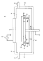
- FIGURE of the drawing is a schematic sectional view of a plasma CVD apparatus in which the method in accordance with the present invention can be carried out.
- a body such as of glass, silicon or other semiconductor material
- the body is placed in a deposition chamber on a susceptor.
- a flow of a deposition gas or mixture of gases is admitted into the deposition chamber and a voltage is applied between an electrode and the susceptor, which are spaced apart.
- the voltage provides sufficient rf power applied to the deposition gas which, at the pressure of the deposition gas, generates a plasma in the gas.
- the plasma causes the gas to react and deposit the desired layer on a surface of the body.
- a power of between about 0.15 and 0.8 watts/cm 2 is used to form the plasma in the deposition gas.
- the total power is determined by the area of the electrode to which the voltage is applied to form the plasma.
- an inactive gas is defined as one which does not adversely affect the body or any coatings thereon and which does not result in an additional coating(s) being applied to the body.
- gases typically include hydrogen (H 2 ), argon (Ar), nitrogen (N 2 ) and ammonia (NH 3 ).
- a power is applied to the inactive gas to cause a plasma to be formed.
- the power applied to the inactive gas is preferably less than that which is used to form the plasma in the deposition gas, i.e., less than 0.15 watts/cm 2 and preferably between 0.03 and 0.14 watts/cm 2 .
- the amount of time that the coated body is subjected to the plasma of the inactive gas can be as little as about two seconds, but is preferably between 5 and 15 seconds. Longer times are allowable.
- the layer is then deposited on the treated body in the manner described hereinabove.
- the plasma of the inactive gas is maintained while the power is increased and the flow of the deposition gas is provided in the deposition chamber to convert the plasma to that of the deposition gas.
- the body is substantially continuously subjected to a plasma while switching from the inactive gas to the deposition gas.
- depositing the layer on the treated body provides an improved interface between the layer and the body so as to achieve improved adherence between the layer and the body.
- the improved interface is evidenced by less haze and fewer bubbles in the deposited layer.
- the plasma of the inactive gas continuously followed by the plasma of the deposition gas prevents any contaminants from accumulating on the surface being coated to improve the interface between the layer and the surface.
- the already deposited layer is subjected to the plasma of the inactive gas prior to depositing the additional layer. This provides an improved interface between the additional deposited layer and the previously deposited layer.
- the use of lower power to form the plasma in the inactive gas is preferable since it prevents damage to the surface being coated, particularly if the surface is of another layer.
- Apparatus 10 comprises a deposition chamber 12 having a top wall 14 with an opening therethrough and a first electrode 16 within the opening.
- the top wall 14 can be solid with the electrode 16 being adjacent either the inner or outer surface thereof.
- a susceptor 18 in the form of a plate which extends parallel to the first electrode 16.
- the susceptor 18 is typically of aluminum and is coated with a layer of aluminum oxide.
- the susceptor 18 is connected to ground so that it serves as a second electrode.
- the susceptor 18 is mounted on the end of a shaft 20 which extends vertically through a bottom wall 22 of the deposition chamber 12.
- the shaft 20 is movable vertically so as to permit the movement of the susceptor 18 vertically toward and away from the first electrode 16.
- a lift-off plate 24 extends horizontally between the susceptor 18 and the bottom wall 22 of the deposition chamber 12 substantially parallel to the susceptor 18.
- Lift-off pins 26 project vertically upwardly from the lift-off plate 24.
- the lift-off pins 26 are positioned to be able to extend through holes 28 in the susceptor 18, and are of a length slightly longer than the thickness of the susceptor 18.
- An outlet pipe 30 extends through a side wall 32 of the deposition chamber 12 and is connected to means (not shown) for evacuating the deposition chamber 12.
- An inlet pipe 34 also extends through another portion of the outer wall 32 of the deposition chamber 12, and is connected through a gas switching network (not shown) to sources (not shown) of various gasses.
- the first electrode 16 is connected to an electrical power source 36.
- a transfer plate (not shown) is typically provided to carry bodies through a load-lock door (not shown) and into the deposition chamber 12 and onto the susceptor 18, and to remove the coated bodies from the deposition chamber 12.
- a body 38 is fed into the deposition chamber 12 and is placed on the susceptor 18 by the transfer plate (not shown).
- the body 38 is of a size to extend over the holes 28 in the susceptor 18.
- the susceptor 18 is positioned above the lift-off pins 26 (as is shown) by moving shaft 20 upwards such that the lift-off pins 26 do not extend through the holes 28, and the susceptor 18 and body 38 are relatively close to the first electrode 16.
- the deposition chamber 12 is evacuated through the outlet pipe 30, and an inactive gas, such as hydrogen, nitrogen, argon or ammonia, is provided into the deposition chamber 12.
- the pressure in the deposition chamber is set at between 26.7 and 466.6 Pa (0.2 and 3.5 Torr).
- the electrical power source 36 is turned on to provide rf power between the first electrode 16 and the susceptor 18 and through the inactive gas.
- the power is preferably between 0.03 and 0.14 watts/cm 2 , with the total power being based on the area of overlap between the electrode 16 and the susceptor 18, and is sufficient to generate a plasma in the inert gas.
- the body 38 is subjected to the plasma of the inactive gas for at least two seconds, and preferably about 10 seconds.
- the power between the electrode 16 and susceptor 18 is increased to a level of typically between 0.15 and 0.8 watts/cm 2 . This maintains the plasma of the inactive gas.
- a deposition gas is then fed into the deposition chamber 12 through the inlet pipe 34 to replace the inactive gas.
- the pressure in the deposition chamber is maintained at about 200 Pa (1.5 Torr).
- the power between the electrode 16 and susceptor 18 is sufficient to now generate a plasma in the deposition gas.
- the plasma causes the deposition gas to decompose and deposit a layer of a desired material on the surface of the body 38.
- the body 38 is continuously subjected to a plasma while the gas is switched from the inactive gas to the deposition gas.
- the composition of the deposition gas depends on the material to be deposited. For example, to deposit silicon nitride (Si 3 N 4 ), a deposition gas comprising a mixture of silane (SiH 4 ), ammonia (NH 3 ), and nitrogen (N 2 ) is used. To deposit a layer of amorphous silicon, a deposition gas comprising a mixture of silane (SiH 4 ) and hydrogen (H 2 ) is used. To deposit silicon oxide (SiO 2 ), a deposition gas comprising a mixture of silane (SiH 4 ) and nitrous oxide (N 2 O) can be used.
- One of the gases used in the deposition gas mixture is often an inactive gas which is also used in the initial treatment of the body 38. If this is so, it is only necessary after the initial treatment to add to the flow of the inactive gas the other gas(es) which form the deposition gas mixture to achieve the deposition of the desired layer.
- the first layer is then subjected to a plasma of an inactive gas. This is done in the same manner as described above for treating the body 38 prior to depositing the first layer.
- the second layer is then deposited on the first layer in the same manner as described above with regard to the first layer. Any number of layers can be deposited on the body 38 in succession. However, before depositing each layer, the previous layer is subjected a plasma of an inactive gas. It is preferred to maintain the plasma in the deposition chamber when switching from one gas to another, i.e., inactive gas to deposition gas or deposition gas to inactive gas.
- the treatment of the body 38 and each layer improves the interface between a deposited layer and either the body surface or a previously deposited layer so as to improve the adhesion therebetween. This improvement is indicated by a layer having an appearance which is less hazy and/or has less bubbles therein.
- the shaft 20 is moved downwardly to move the susceptor 18 and coated body 38 away from the first electrode 16 and toward the lift-off plate 24.
- the lift-off pins 26 extend through the holes 28 until they engage a bottom surface 38a of the body 38. Since the lift-off fins 26 are longer than the thickness of the susceptor 18, the lift-off pins 26 stop the downward movement of the body 38. Further downward movement of the susceptor 18 causes the separation of the body 38 from the susceptor 18.
- the coated body 38 is then picked up by the transfer plate (not shown) and removed from the deposition chamber 12.
- the electrode 16 and susceptor 18 are each 38 x 48 cm.
- a glass plate which is the body 38, was transferred into a deposition chamber 12 and placed on the susceptor 18.
- the susceptor 18 was moved upwardly until there was a spacing of 962 mils (24 mm) between the susceptor 18 and an electrode 16.
- a flow of hydrogen gas was provided into the deposition chamber and a pressure of 106.7 Pa (0.8 Torr) was achieved.
- the power source 36 to the electrode 16 was turned on and rf power of 300 watts was provided. This created a plasma in the hydrogen gas.
- the glass plate was subjected to the hydrogen plasma for 10 seconds.
- the power to the electrode 16 was increased to 1200 watts which maintained the plasma of hydrogen.
- the flow of hydrogen gas was then replaced with a flow of a deposition gas comprising a mixture of silane, ammonia and nitrogen and a pressure of 200 Pa (1.5 Torr) was was achieved.
- the susceptor 18 was maintained at a spacing of 962 mils (24 mm) from the electrode 16.
- the power to the electrode 16 was sufficient to result in a plasma being achieved in the deposition gas mixture.
- the plasma caused the silane and ammonia to react and deposit a layer is silicon nitride on the surface of the glass plate.
- the flow of the deposition gas was stopped, the power turned off and the coated glass plate was removed from the deposition chamber 12.
- the electrode 16 and susceptor 18 are each also 38 x 48 cm.
- a glass plate (which is the body 30) was transferred into the deposition chamber 12 and placed on a susceptor 18. The susceptor was moved upwardly toward an electrode 16 until there was a spacing of 962 mils (24 mm) therebetween.
- a flow of hydrogen was provided into the deposition chamber and a pressure of 106.7 Pa (0.8 Torr) was achieved.
- the power source 36 was turned on to obtain a power of 250 watts between the electrode 16 and susceptor 18. This resulted in the formation of a plasma in the hydrogen.
- the glass plate was subjected to the plasma of hydrogen for 10 seconds.
- the power to the electrode 16 was increased to 1200 watts which maintained the plasma of hydrogen.
- the flow of hydrogen was then replaced with the flow of a deposition gas comprising a mixture of silane, ammonia and nitrogen.
- the pressure of the deposition gas was set at 200 Pa (1.5 Torr) and the spacing between the electrode 16 and susceptor 18 was maintained at 962 mils (24 mm).
- the power to the electrode 16 was sufficient to result in the formation of a plasma in the deposition gas which caused the deposition gas to react and deposit a layer of silicon nitride on the surface of the glass plate.
- the power to the electrode 16 was decreased to 250 watts which was still sufficient to maintain a plasma of the deposition gas.
- the flow of the deposition gas was replaced with a flow of hydrogen which was maintained at a pressure of 106.7 Pa (0.8 Torr).
- the spacing between the electrode 16 and susceptor 18 was maintained at 962 mils (24 mm).
- the power to the electrode 16 was sufficient to generate a plasma in the hydrogen.
- the glass plate with the coating of silicon nitride thereon was subjected to the hydrogen plasma for 10 seconds.
- the power to the electrode 16 was then increased to 250-300 watts which maintained the plasma of the hydrogen.
- the flow of only hydrogen was replaced with a flow of a second deposition gas comprising a mixture of silane and hydrogen which was set at a pressure of 106.7 Pa (0.8 Torr).
- the spacing between the electrode 16 and susceptor 18 was maintained at 962 mils (24 mm).
- the power to the electrode 16 was sufficient to generate a plasma in the second deposition gas.
- the plasma caused the silane to react to deposit a layer of amorphous silicon on the silicon nitride layer.
- the flow of the second deposition gas was stopped, the power source turned off, and the coated glass plate was removed from the deposition chamber 12.
- a method of treating a surface on which a layer is to be deposited by plasma CVD so as to improve the interface between the surface and the layer can be that of a body with the layer being deposited directly on a surface thereof, or can be that of a first layer on a body with a second layer being deposited on the first layer.
- the improved interface is achieved by treating the body in a plasma of an inactive gas which does not adversely affect the body and which does not in itself deposit a layer on the body.
- the improved interface is visually indicated by reduced haze and/or bubbles being formed on the layer which is deposited on the body.
- inactive gases other than those listed above may be used as long as they can form a plasma and do not adversely affect the body or layer on which the layer is to be deposited, and do not in themselves deposit a layer on the body.
- substrate bodies of material other than those listed above can be used.
Landscapes
- Chemical & Material Sciences (AREA)
- Engineering & Computer Science (AREA)
- Physics & Mathematics (AREA)
- Plasma & Fusion (AREA)
- General Chemical & Material Sciences (AREA)
- Chemical Kinetics & Catalysis (AREA)
- Materials Engineering (AREA)
- Mechanical Engineering (AREA)
- Metallurgy (AREA)
- Organic Chemistry (AREA)
- Chemical Vapour Deposition (AREA)
- Drying Of Semiconductors (AREA)
Claims (7)
- Procédé de croissance d'une structure au moyen d'un dépôt en phase vapeur activé par plasma, comprenant les étapes constituées de :un positionnement d'un substrat sur un emplacement de traitement dans une chambre réactionnelle (12) à plasma,une première étape consistant à faire s'écouler un premier gaz jusque dans ladite chambre (12) et à l'exciter en un plasma afin de déposer une couche de nitrure de silicium sur ledit substrat placé audit emplacement de traitement,une seconde étape consistant à faire circuler un gaz inerte jusque dans ladite chambre (12) et à l'exciter en un plasma afin de traiter une surface de ladite couche de nitrure de silicium pendant que ledit substrat est placé audit emplacement de traitement,une troisième étape consistant à faire circuler un troisième gaz jusque dans ladite chambre et à l'exciter en un plasma afin de déposer une couche de silicium amorphe sur ladite couche de nitrure de silicium pendant que ledit substrat est placé audit emplacement de traitement,grâce à quoi le traitement par plasma inerte de la seconde étape améliore l'interface entre la couche de nitrure de silicium et la couche de silicium.
- Procédé selon la revendication 1, dans lequelladite première étape comprend l'application d'un premier niveau de puissance HF à ladite chambre,ladite seconde étape comprend l'application d'un second niveau de puissance HF à ladite chambre,ladite troisième étape comprend l'application d'un troisième niveau de puissance HF à ladite chambre, etledit second niveau est inférieur auxdits premier et troisième niveaux.
- Procédé selon la revendication 1 ou 2,
dans lequel ledit second gaz inerte est constitué essentiellement d'un gaz choisi parmi le groupe constitué de l'hydrogène, de l'azote, de l'argon et de l'ammoniac. - Procédé selon la revendication 3,
dans lequel ledit second gaz inerte est constitué d'hydrogène. - Procédé selon les revendications 1 à 4,
dans lequel ledit premier gaz comprend du silane, de l'ammoniac et de l'azote et ledit second gaz comprend du silane et de l'hydrogène. - Procédé selon les revendications 1 à 5, dans lequel lesdites première, seconde et troisième étapes entretiennent sans interruption un plasma dans ladite chambre (12).
- Procédé selon les revendications 1 à 6, comprenant en outre une étape réalisée avant ladite première étape, constituant à faire s'écouler un quatrième gaz inerte jusque dans ladite chambre (12) et à l'exciter en un plasma afin de traiter une surface dudit substrat.
Applications Claiming Priority (2)
| Application Number | Priority Date | Filing Date | Title |
|---|---|---|---|
| US8001993A | 1993-06-21 | 1993-06-21 | |
| US80019 | 1993-06-21 |
Publications (3)
| Publication Number | Publication Date |
|---|---|
| EP0630989A2 EP0630989A2 (fr) | 1994-12-28 |
| EP0630989A3 EP0630989A3 (fr) | 1996-01-03 |
| EP0630989B1 true EP0630989B1 (fr) | 2000-01-12 |
Family
ID=22154736
Family Applications (1)
| Application Number | Title | Priority Date | Filing Date |
|---|---|---|---|
| EP94109547A Expired - Lifetime EP0630989B1 (fr) | 1993-06-21 | 1994-06-21 | Procédé pour le plasma-dépôt chimique en phase vapeur de souches ayant une interface améliorée |
Country Status (4)
| Country | Link |
|---|---|
| EP (1) | EP0630989B1 (fr) |
| JP (1) | JPH07142416A (fr) |
| KR (1) | KR100326488B1 (fr) |
| DE (1) | DE69422550T2 (fr) |
Cited By (3)
| Publication number | Priority date | Publication date | Assignee | Title |
|---|---|---|---|---|
| US6794311B2 (en) | 2000-07-14 | 2004-09-21 | Applied Materials Inc. | Method and apparatus for treating low k dielectric layers to reduce diffusion |
| US7144606B2 (en) | 1999-06-18 | 2006-12-05 | Applied Materials, Inc. | Plasma treatment to enhance adhesion and to minimize oxidation of carbon-containing layers |
| US7229911B2 (en) | 2004-04-19 | 2007-06-12 | Applied Materials, Inc. | Adhesion improvement for low k dielectrics to conductive materials |
Families Citing this family (20)
| Publication number | Priority date | Publication date | Assignee | Title |
|---|---|---|---|---|
| US6291343B1 (en) | 1994-11-14 | 2001-09-18 | Applied Materials, Inc. | Plasma annealing of substrates to improve adhesion |
| FR2756663B1 (fr) * | 1996-12-04 | 1999-02-26 | Berenguer Marc | Procede de traitement d'un substrat semi-conducteur comprenant une etape de traitement de surface |
| US6872429B1 (en) | 1997-06-30 | 2005-03-29 | Applied Materials, Inc. | Deposition of tungsten nitride using plasma pretreatment in a chemical vapor deposition chamber |
| US6162715A (en) | 1997-06-30 | 2000-12-19 | Applied Materials, Inc. | Method of forming gate electrode connection structure by in situ chemical vapor deposition of tungsten and tungsten nitride |
| US20010049181A1 (en) | 1998-11-17 | 2001-12-06 | Sudha Rathi | Plasma treatment for cooper oxide reduction |
| US6355571B1 (en) | 1998-11-17 | 2002-03-12 | Applied Materials, Inc. | Method and apparatus for reducing copper oxidation and contamination in a semiconductor device |
| JP2001044187A (ja) * | 1999-07-30 | 2001-02-16 | Furontekku:Kk | プラズマ成膜方法および半導体装置の製造装置 |
| KR100467082B1 (ko) * | 2000-03-02 | 2005-01-24 | 주성엔지니어링(주) | 반도체소자 제조장치 및 그 클리닝방법 |
| CN1322556C (zh) * | 2001-02-15 | 2007-06-20 | 东京毅力科创株式会社 | 被处理件的处理方法及处理装置 |
| JP4573162B2 (ja) * | 2004-09-16 | 2010-11-04 | 富士電機システムズ株式会社 | 透明導電膜の製造方法 |
| KR100710597B1 (ko) * | 2004-12-08 | 2007-04-24 | 주식회사 에이디피엔지니어링 | 플라즈마 처리장치 |
| ITMI20092107A1 (it) * | 2009-11-30 | 2011-06-01 | Milano Politecnico | Metodo e apparato per la deposizione di strati sottili nanostrutturati con morfologia e nanostruttura controllata |
| GB201218697D0 (en) * | 2012-10-18 | 2012-11-28 | Spts Technologies Ltd | A method of depositing an amorphous silicon film |
| CN107464743A (zh) * | 2017-07-17 | 2017-12-12 | 上海华虹宏力半导体制造有限公司 | 非晶硅薄膜成膜方法 |
| CN107919272A (zh) * | 2017-11-21 | 2018-04-17 | 上海华虹宏力半导体制造有限公司 | 非晶硅薄膜成膜方法 |
| CN109148263A (zh) * | 2018-07-26 | 2019-01-04 | 上海华虹宏力半导体制造有限公司 | 沉积非晶硅的成膜方法 |
| CN109166795A (zh) * | 2018-08-20 | 2019-01-08 | 上海华虹宏力半导体制造有限公司 | TiN电极薄膜形成方法 |
| CN109285759B (zh) * | 2018-09-11 | 2021-08-20 | 上海华虹宏力半导体制造有限公司 | 非晶硅的成膜方法 |
| KR102903090B1 (ko) * | 2019-07-19 | 2025-12-19 | 에이에스엠 아이피 홀딩 비.브이. | 토폴로지-제어된 비정질 탄소 중합체 막을 형성하는 방법 |
| CN114664651B (zh) * | 2020-12-23 | 2025-01-10 | 长鑫存储技术有限公司 | 半导体表面缺陷的处理方法和半导体器件的制备方法 |
Family Cites Families (6)
| Publication number | Priority date | Publication date | Assignee | Title |
|---|---|---|---|---|
| JPS5821324A (ja) * | 1981-07-30 | 1983-02-08 | Agency Of Ind Science & Technol | 水素添加した半導体薄膜成長用金属表面基板の前処理方法 |
| DE3574997D1 (de) * | 1984-03-03 | 1990-02-01 | Stc Plc | Pulsierendes plasmaverfahren. |
| CH671407A5 (fr) * | 1986-06-13 | 1989-08-31 | Balzers Hochvakuum | |
| DE4005956C1 (fr) * | 1990-02-26 | 1991-06-06 | Siegfried Dipl.-Ing. Dr. 5135 Selfkant De Straemke | |
| FR2664294B1 (fr) * | 1990-07-06 | 1992-10-23 | Plasmametal | Procede de metallisation d'une surface. |
| DE4034842A1 (de) * | 1990-11-02 | 1992-05-07 | Thyssen Edelstahlwerke Ag | Verfahren zur plasmachemischen reinigung fuer eine anschliessende pvd oder pecvd beschichtung |
-
1994
- 1994-06-20 KR KR1019940013880A patent/KR100326488B1/ko not_active Expired - Fee Related
- 1994-06-20 JP JP6137629A patent/JPH07142416A/ja active Pending
- 1994-06-21 DE DE69422550T patent/DE69422550T2/de not_active Expired - Fee Related
- 1994-06-21 EP EP94109547A patent/EP0630989B1/fr not_active Expired - Lifetime
Cited By (3)
| Publication number | Priority date | Publication date | Assignee | Title |
|---|---|---|---|---|
| US7144606B2 (en) | 1999-06-18 | 2006-12-05 | Applied Materials, Inc. | Plasma treatment to enhance adhesion and to minimize oxidation of carbon-containing layers |
| US6794311B2 (en) | 2000-07-14 | 2004-09-21 | Applied Materials Inc. | Method and apparatus for treating low k dielectric layers to reduce diffusion |
| US7229911B2 (en) | 2004-04-19 | 2007-06-12 | Applied Materials, Inc. | Adhesion improvement for low k dielectrics to conductive materials |
Also Published As
| Publication number | Publication date |
|---|---|
| DE69422550D1 (de) | 2000-02-17 |
| KR100326488B1 (ko) | 2002-06-20 |
| EP0630989A2 (fr) | 1994-12-28 |
| JPH07142416A (ja) | 1995-06-02 |
| EP0630989A3 (fr) | 1996-01-03 |
| DE69422550T2 (de) | 2000-08-10 |
| KR950000922A (ko) | 1995-01-03 |
Similar Documents
| Publication | Publication Date | Title |
|---|---|---|
| EP0630989B1 (fr) | Procédé pour le plasma-dépôt chimique en phase vapeur de souches ayant une interface améliorée | |
| EP0630990B1 (fr) | Procédé pour limiter l'adhésivité d'un corps sur un support dans un traitement de dépÔt | |
| KR100355321B1 (ko) | 성막방법및장치 | |
| US8337960B2 (en) | Seasoning method for film-forming apparatus | |
| US7589017B2 (en) | Methods for growing low-resistivity tungsten film | |
| EP1672093B1 (fr) | Appareil et procede de formation de films | |
| KR20210094462A (ko) | 전처리를 사용하여 실리콘 질화물 층을 증착하는 방법, 상기 방법을 사용하여 형성된 구조체, 및 상기 방법을 수행하기 위한 시스템 | |
| US5906866A (en) | Process for chemical vapor deposition of tungsten onto a titanium nitride substrate surface | |
| US20040202786A1 (en) | Method of forming low-resistivity tungsten interconnects | |
| US20060264038A1 (en) | Method for forming barrier film and method for forming electrode film | |
| US5510297A (en) | Process for uniform deposition of tungsten silicide on semiconductor wafers by treatment of susceptor having aluminum nitride surface thereon with tungsten silicide after cleaning of susceptor | |
| EP1138801B1 (fr) | Procédé de formation d'un film mince sur un substrat semi-conducteur | |
| JP2802865B2 (ja) | プラズマcvd装置 | |
| US6911233B2 (en) | Method for depositing thin film using plasma chemical vapor deposition | |
| WO2022159883A1 (fr) | Procédé de remplissage d'espace utilisant un plasma radiofréquence à haute fréquence pulsée (hfrf) | |
| US6271121B1 (en) | Process for chemical vapor deposition of tungsten onto a titanium nitride substrate surface | |
| JPH09320963A (ja) | Cvdチャンバを清掃した後に調整するための方法 | |
| JP2024544271A (ja) | 2次元層状材料に材料を堆積する方法 | |
| JP2776807B2 (ja) | 半導体装置の製造方法 | |
| CN1467303A (zh) | 利用等离子体化学气相沉积法沉积薄膜的方法 | |
| CN117721441B (zh) | 一种高应力氮化硅薄膜及其形成方法 | |
| KR100214906B1 (ko) | 디클로로실란과 육플루오르화 텅스텐을 사용하여 반도체 기판상에 규화 텅스텐 박막을 증착시키는 방법 | |
| KR0172857B1 (ko) | 화학기상 증착에 의한 박막형성방법 | |
| US12586764B2 (en) | Plasma showerhead treatment methods | |
| KR102847940B1 (ko) | 기판 처리 장치의 시즈닝 박막 형성 방법 |
Legal Events
| Date | Code | Title | Description |
|---|---|---|---|
| PUAI | Public reference made under article 153(3) epc to a published international application that has entered the european phase |
Free format text: ORIGINAL CODE: 0009012 |
|
| AK | Designated contracting states |
Kind code of ref document: A2 Designated state(s): DE FR GB IT NL |
|
| RIN1 | Information on inventor provided before grant (corrected) |
Inventor name: MAYDAN, DAN Inventor name: LAW, KAM Inventor name: CONNOLLY, ROBERT Inventor name: FENG, GUOFU JEFF Inventor name: TAKEHARA, TAKAKO Inventor name: LEE, ANGELA T. Inventor name: KOLLRACK, MARC MICHAEL Inventor name: ROBERTSON, ROBERT |
|
| PUAL | Search report despatched |
Free format text: ORIGINAL CODE: 0009013 |
|
| AK | Designated contracting states |
Kind code of ref document: A3 Designated state(s): DE FR GB IT NL |
|
| 17P | Request for examination filed |
Effective date: 19960703 |
|
| 17Q | First examination report despatched |
Effective date: 19980629 |
|
| GRAG | Despatch of communication of intention to grant |
Free format text: ORIGINAL CODE: EPIDOS AGRA |
|
| GRAG | Despatch of communication of intention to grant |
Free format text: ORIGINAL CODE: EPIDOS AGRA |
|
| GRAH | Despatch of communication of intention to grant a patent |
Free format text: ORIGINAL CODE: EPIDOS IGRA |
|
| GRAH | Despatch of communication of intention to grant a patent |
Free format text: ORIGINAL CODE: EPIDOS IGRA |
|
| GRAA | (expected) grant |
Free format text: ORIGINAL CODE: 0009210 |
|
| AK | Designated contracting states |
Kind code of ref document: B1 Designated state(s): DE FR GB IT NL |
|
| REF | Corresponds to: |
Ref document number: 69422550 Country of ref document: DE Date of ref document: 20000217 |
|
| ITF | It: translation for a ep patent filed | ||
| ET | Fr: translation filed | ||
| PLBE | No opposition filed within time limit |
Free format text: ORIGINAL CODE: 0009261 |
|
| STAA | Information on the status of an ep patent application or granted ep patent |
Free format text: STATUS: NO OPPOSITION FILED WITHIN TIME LIMIT |
|
| 26N | No opposition filed | ||
| REG | Reference to a national code |
Ref country code: GB Ref legal event code: IF02 |
|
| PGFP | Annual fee paid to national office [announced via postgrant information from national office to epo] |
Ref country code: GB Payment date: 20020610 Year of fee payment: 9 |
|
| PGFP | Annual fee paid to national office [announced via postgrant information from national office to epo] |
Ref country code: FR Payment date: 20020614 Year of fee payment: 9 |
|
| PGFP | Annual fee paid to national office [announced via postgrant information from national office to epo] |
Ref country code: NL Payment date: 20020628 Year of fee payment: 9 Ref country code: DE Payment date: 20020628 Year of fee payment: 9 |
|
| PG25 | Lapsed in a contracting state [announced via postgrant information from national office to epo] |
Ref country code: GB Free format text: LAPSE BECAUSE OF NON-PAYMENT OF DUE FEES Effective date: 20030621 |
|
| PG25 | Lapsed in a contracting state [announced via postgrant information from national office to epo] |
Ref country code: NL Free format text: LAPSE BECAUSE OF NON-PAYMENT OF DUE FEES Effective date: 20040101 Ref country code: DE Free format text: LAPSE BECAUSE OF NON-PAYMENT OF DUE FEES Effective date: 20040101 |
|
| GBPC | Gb: european patent ceased through non-payment of renewal fee |
Effective date: 20030621 |
|
| PG25 | Lapsed in a contracting state [announced via postgrant information from national office to epo] |
Ref country code: FR Free format text: LAPSE BECAUSE OF NON-PAYMENT OF DUE FEES Effective date: 20040227 |
|
| NLV4 | Nl: lapsed or anulled due to non-payment of the annual fee |
Effective date: 20040101 |
|
| REG | Reference to a national code |
Ref country code: FR Ref legal event code: ST |
|
| PG25 | Lapsed in a contracting state [announced via postgrant information from national office to epo] |
Ref country code: IT Free format text: LAPSE BECAUSE OF NON-PAYMENT OF DUE FEES Effective date: 20050621 |