EP0631304A2 - System und Methode zur Kontrolle und Evaluierung einer Halbleiterscheibenfabrikation - Google Patents
System und Methode zur Kontrolle und Evaluierung einer Halbleiterscheibenfabrikation Download PDFInfo
- Publication number
- EP0631304A2 EP0631304A2 EP94107133A EP94107133A EP0631304A2 EP 0631304 A2 EP0631304 A2 EP 0631304A2 EP 94107133 A EP94107133 A EP 94107133A EP 94107133 A EP94107133 A EP 94107133A EP 0631304 A2 EP0631304 A2 EP 0631304A2
- Authority
- EP
- European Patent Office
- Prior art keywords
- semiconductor wafer
- evaluating
- location
- wafer
- locations
- Prior art date
- Legal status (The legal status is an assumption and is not a legal conclusion. Google has not performed a legal analysis and makes no representation as to the accuracy of the status listed.)
- Granted
Links
Images

Classifications
-
- H—ELECTRICITY
- H10—SEMICONDUCTOR DEVICES; ELECTRIC SOLID-STATE DEVICES NOT OTHERWISE PROVIDED FOR
- H10P—GENERIC PROCESSES OR APPARATUS FOR THE MANUFACTURE OR TREATMENT OF DEVICES COVERED BY CLASS H10
- H10P74/00—Testing or measuring during manufacture or treatment of wafers, substrates or devices
- H10P74/23—Testing or measuring during manufacture or treatment of wafers, substrates or devices characterised by multiple measurements, corrections, marking or sorting processes
-
- B—PERFORMING OPERATIONS; TRANSPORTING
- B24—GRINDING; POLISHING
- B24B—MACHINES, DEVICES, OR PROCESSES FOR GRINDING OR POLISHING; DRESSING OR CONDITIONING OF ABRADING SURFACES; FEEDING OF GRINDING, POLISHING, OR LAPPING AGENTS
- B24B37/00—Lapping machines or devices; Accessories
- B24B37/005—Control means for lapping machines or devices
- B24B37/013—Devices or means for detecting lapping completion
-
- H—ELECTRICITY
- H10—SEMICONDUCTOR DEVICES; ELECTRIC SOLID-STATE DEVICES NOT OTHERWISE PROVIDED FOR
- H10P—GENERIC PROCESSES OR APPARATUS FOR THE MANUFACTURE OR TREATMENT OF DEVICES COVERED BY CLASS H10
- H10P74/00—Testing or measuring during manufacture or treatment of wafers, substrates or devices
- H10P74/23—Testing or measuring during manufacture or treatment of wafers, substrates or devices characterised by multiple measurements, corrections, marking or sorting processes
- H10P74/238—Testing or measuring during manufacture or treatment of wafers, substrates or devices characterised by multiple measurements, corrections, marking or sorting processes comprising acting in response to an ongoing measurement without interruption of processing, e.g. endpoint detection or in-situ thickness measurement
-
- H—ELECTRICITY
- H10—SEMICONDUCTOR DEVICES; ELECTRIC SOLID-STATE DEVICES NOT OTHERWISE PROVIDED FOR
- H10P—GENERIC PROCESSES OR APPARATUS FOR THE MANUFACTURE OR TREATMENT OF DEVICES COVERED BY CLASS H10
- H10P74/00—Testing or measuring during manufacture or treatment of wafers, substrates or devices
- H10P74/27—Structural arrangements therefor
-
- H—ELECTRICITY
- H10—SEMICONDUCTOR DEVICES; ELECTRIC SOLID-STATE DEVICES NOT OTHERWISE PROVIDED FOR
- H10P—GENERIC PROCESSES OR APPARATUS FOR THE MANUFACTURE OR TREATMENT OF DEVICES COVERED BY CLASS H10
- H10P74/00—Testing or measuring during manufacture or treatment of wafers, substrates or devices
- H10P74/20—Testing or measuring during manufacture or treatment of wafers, substrates or devices characterised by the properties tested or measured, e.g. structural or electrical properties
- H10P74/203—Structural properties, e.g. testing or measuring thicknesses, line widths, warpage, bond strengths or physical defects
Definitions
- This invention relates to integrated circuits, and more particularly relates to monitoring and evaluating uniformity of semiconductor wafer fabrication processes.
- Various processes and procedures are used to fabricate integrated circuits on semiconductor wafers. Examples of these processes include oxidation of silicon to form a silicon dioxide (SiO2) film on a silicon substrate and microlithography which generally involves placing a radiation sensitive material (sometimes referred to as a "photoresist” or “resist”) on the oxide film. Structural features of the integrated circuit are frequently developed on the wafer by either depositing material, oxidation, or removing the underlying material (etching). Typically, the resist is radiated through a mask placed over the resist by lithography techniques such as photolithography, electron beam lithography or x-ray lithography. The resist reacts chemically in the exposed areas of the mask depending upon the choice of the chemical system.
- lithography techniques such as photolithography, electron beam lithography or x-ray lithography.
- the sequence of wafer fabrication processes and procedures are selected depending upon the type of semiconductor wafer and the desired operating characteristics of the integrated circuit which will be fabricated on the semiconductor wafer. Fabrication processes are frequently repeated several times to build up multiple layers associated with modern very large scale integrated circuits which are fabricated on semiconductor wafers.
- Etching is a commonly used process in the fabrication of many integrated circuits on semiconductor wafers having a silicon substrate. Etching involves removal of material from the silicon substrate and/or selected thin film layers which were previously deposited on the surface of the silicon substrate. When a mask is used to protect portions of the wafer surface, the goal of etching is to remove material which is not covered by the mask. The primary objective of the etching process is to precisely transfer the pattern established by the protective mask onto the underlying material.
- Ellipsometry also measures the optical index of refraction. Ellipsometry techniques are frequently used to measure the thickness and index of refraction of various types of dialectic films and also determine the thickness of multiple layer film structures such as polysilicon on silicon dioxide or a photoresist on silicon dioxide. Other techniques for determining film thickness include optical interference, capacitance methods and/or oxide film color charts.
- the present invention allows monitoring a fabrication process at a selected site on a semiconductor wafer and reliably predicting the results of the fabrication process at other sites on the semiconductor wafer.
- the present invention allows a fabrication process to be monitored in situ at a selected location on a semiconductor wafer and to reliably predict the results of the fabrication process at other locations on the semiconductor wafer as a function of information obtained at the selected location and process conditions or control factors. With proper modeling and specification of the process conditions or control factors, real-time evaluation of a fabrication process across the fall wafer surface is now available.
- statistical modeling methods are combined with in situ ellipsometry to provide real time evaluation of spatial etch rate patterns across the surface of a semiconductor wafer as a function of selected process conditions during a single wafer plasma etch fabrication process.
- real time evaluation of the etch rate at other sites or locations across the surface of the wafer variations between wafers fabricated in the same reactor vessel with the same process are substantially reduced by providing enhanced run-to-run control.
- An important technical feature of the present invention is reducing surface damage and achieving desired vertical profiles during selective etching of polysilicon.
- the present invention provides improved process control to enhance uniformity of the polysilicon layer across the surface of a semiconductor wafer during the bulk etching process.
- the present invention provides information to achieve optimum, uniform thickness of a polysilicon layer after completion of the bulk etch process.
- the present invention also controls etch uniformity on a wafer to wafer basis.
- Another important technical feature of the present invention includes taking information obtained from a sensor monitoring one location on the surface of a semiconductor during a fabrication process and using the information to provide real time evaluation of the results of the process at any other desired location on the surface of the semiconductor wafer.
- Information provided by the sensor may be used to control and/or stop the fabrication process when inferred values at other locations on the surface of the semiconductor wafer indicate a desired level of uniformity across the wafer surface.
- FIGURES 1 through 6 of the drawings like numerals being used for like and corresponding parts of the various drawings.
- Various processes such as oxidation, diffusion, ion implantation, chemical vapor deposition and etching are used during the fabrication of an integrated circuit on a semiconductor wafer.
- various types of in situ sensors such as interferometers, infrared spectrometers, laser interferometers and ellipsometers are used to monitor selected fabrication processes appropriate for each type of sensor.
- Semiconductor wafer 40 is preferably a thin slice from a single crystal of semiconductor material such as silicon.
- the present invention may be used with other types of semiconductor materials and is not limited to silicon.
- semiconductor wafer 40 having a silicon substrate and one or more film layers is disposed on quartz pins 26 within reactor vessel or reagent chamber 28.
- Ellipsometer 20 includes laser light source 22 and analyzer 24.
- Reagent chamber 28 will preferably include two or more optical windows (not shown) to allow ellipsometer 20 to measure the thickness of a film layer or layers at selected site 44 on surface 42 of wafer 40.
- Reagent chamber 28 may include both an inner chamber (not shown) and an outer chamber.
- Ellipsometer 20 measures changes in polarized light as the light is reflected and transmitted through thin film layers on surface 42 of semiconductor wafer 40. Ellipsometer 20 is preferably designed to calculate the thickness and index of refraction from a polysilicon layer every 0.5 seconds.
- surface 42 of semiconductor wafer 40 has been divided into approximately sixty-seven dies or potential sites for fabricating integrated circuits (not shown) on surface 42 of semiconductor wafer 40.
- Various lithography processes may be used to fabricate integrated circuits on wafer 40.
- integrated circuits are typically built in a series of layers on the respective dies on surface 42.
- the integrated circuits or portions of the integrated circuit may be fabricated on each die by processes such as etching or oxidation.
- Ellipsometer 20 is preferably aligned to measure the thickness of a polysilicon film layer (not shown) on die 44.
- Die 44 may also be referred to by its coordinates (6,5), or as the ellipsometer site.
- ellipsometry systems such as ellipsometer 20 are generally only capable of measuring film thickness over a relatively small sampling area.
- An in situ sampling site such as die 44, provides no on-line capability to observe the thickness of the film layer at other locations on the surface of the semiconductor wafer. Therefore, previously available ellipsometer techniques do not allow in situ monitoring and evaluation of a fabrication process such as etching or oxidizing across the full surface 42 of semiconductor wafer 40.
- This same limitation applies to many other sensors used for in situ monitoring of an integrated circuit fabrication process.
- the sensors are limited to providing information concerning only one area on the wafer surface.
- the present invention provides a real time evaluation of a selected fabrication process such as etching at other locations such as die 46 (coordinate location 3,3) or die 48 (coordinate location 6,9).
- This evaluation can be obtained by statistically modelling each site on the surface of wafer 40 as a function of the etch rate measured at ellipsometer site or die 44.
- the spatial model for each site will preferably include selected process conditions or control factors associated with the fabrication process which is being monitored by the sensor.
- Etching thin films uniformly on surface 42 is a critical step to ensure high finished product yield from the fabrication process. Without uniform etching, too much material may be left at some sites on wafer 40 and other sites may be completely etched through the desired film layer with possible removal of underlying layers.
- An important requirement for success of the present invention is to develop a model of the mean etch rate at other locations on wafer surface 42 based on the etch rate measured at die 44 by ellipsometer 20. By developing a model for other locations on surface 42, a better evaluation may be made of the uniformity of the plasma etch process. After the etch rate at a plurality of sites on the wafer surface 42 has been modeled, the models may be optimized to achieve either a uniform distribution of etch rates across wafer surface 42 or a uniform remaining thickness across wafer surface 42.
- Statistical modeling was developed for plasma etching of a single wafer such as semiconductor wafer 40 using in situ ellipsometry to infer real time etch rates at various locations across surface 42 of wafer 40 as a function of process conditions associated with the plasma etching process and the mean etch rate at the ellipsometer site.
- Statistical models describing the fabrication process as a function of process conditions or control factors use an empirical expression such as: to fit the measurable values using least squares regression.
- Y is the measurable response and X i 's are the process conditions or control factors.
- Response surface methodology was used to empirically derive the formula for mean etch rate at the other locations using process conditions or control factors and the mean etch rate measured by ellipsometer 20 as independent variables.
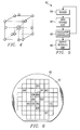
- a rotatable central composite design as represented by FIGURE 4 was selected for three process conditions or control factors used to develop the model for mean etch rate at the other locations.
- the selected control factors were RF power, total pressure in reactor vessel 28 and total flow rate of reactants (HCl + HBr). To ensure statistical reliability twenty separate semiconductor wafers 40 were measured.
- the RF power ranged from 300 to 500 watts, the total pressure was varied between 200 and 400 mTorr, and total flow rate was varied between 75 and 175 SCCM.
- calculator/controller 66 will also contain a second function for converting values of layer thickness measured by ellipsometer 20 into the mean etch rate at ellipsometer site 44. Calculator/controller 66 will then use the first function to derive the mean etch rate at the other locations on surface 42 of wafer 40 based on mean etch rate at ellipsometer site 44 and the value of selected control factors such as RF power, total pressure and total flow rate of the reactants.
- a third function similar to the second function, may be used to convert the mean etch rate at the other locations into thickness of the film layer at the other locations.
- Calculator/controller 66 may be used to supply a signal to output interface unit 68.
- Output interface unit 68 may be used to indicate that the control factors or process conditions should be changed to obtain the desired results of the fabrication process at the other locations on surface 42.
- Calculator/controller 66 may also be used to provide a feedback signal to ellipsometer 20.
- FIGURE 6 demonstrates the results of using the present invention to control the bulk etch rate on surface 42 of semiconductor wafer 40.
- a uniform thickness of +/-300A was obtained across surface 42.
- the bulk etching process was stopped when ellipsometer 20 indicated a thickness of 500A at ellipsometer site 44.
- the thickness of the film layer at the other sites on surface 42 was measured by off-line spectrophotometry and are shown by the numbers in the respective dies.
- control system 60 with appropriate empirical models (first function) for other locations on surface 42 may be used to enhance run by run process controls for reactor vessel 28 in the selected fabrication process.
- Control system 60 may be used to provide the end point for the selected fabrication process based on process conditions or control factors and information provided by in situ sensor 64 that measures the results of the fabrication process at one selected location on the wafer surface.
- Data storage unit 62 and calculator/controller 66 cooperate with each other by using a first function (empirical model for other locations on surface 42) to convert data from sensor 64 into projected results of the fabrication process at other locations on the surface 42.
- control system 60 allows control system 60 to evaluate and monitor the performance of reactor vessel 28 and its associated supporting systems (not shown) during the fabrication of integrated circuits on semiconductor wafer 40.
- Information supplied by output interface unit 68 allows the operator to adjust the control factors for the fabrication process which is being monitored and evaluated when inferred values at the other locations do not indicate the desired results.
- Control system 60 allows adjusting of the control factors to meet the desired target values for the fabrication process at the other sites on surface 42. Thus, the uniformity of the fabrication process on wafer-to-wafer runs within reactor vessel 28 may be enhanced.
- the etching process may be stopped when the inferred values of mean etch rate at the other locations on surface 42 indicate that the desired amount of material has been removed. Alternatively, the etching process may be stopped when the inferred values of thickness at the other locations on surface 42 have been obtained.
- the present invention also allows developing empirical models to accommodate semiconductor wafers which do not have a uniform thickness and/or reactor vessels which have unique patterns for reactivity within the vessel.
- the film on the top half of semiconductor wafer 40 may be thicker than the film on the bottom half.
- reactor vessel 28 may produce a bull's eye effect with enhanced reactivity at the center of surface 42 and less reactivity near the edges of surface 42.
- the present invention has been described with respect to plasma etching of polysilicon thin films. The methods and procedures have potential application for the etching of other films.
- the present invention may be used for the deposition or oxidation of films. In this approach the deposition rate would be modeled as a function of the process conditions and the mean deposition rate measured in situ by ellipsometer 44.
- the present invention had been described with respect to in situ ellipsometry for single-point monitoring of etch rate.
- the modeling method is applicable for use with any sensor that provides real-time data.
- the same methods and procedures may be used for modeling line width reduction during polysilicon etching using an in situ laser diffraction imaging system (not shown).
- physically-based modeling may be used to develop the first function for evaluating a selected fabrication process across surface 42 of wafer 40.
Landscapes
- Engineering & Computer Science (AREA)
- Mechanical Engineering (AREA)
- Testing Or Measuring Of Semiconductors Or The Like (AREA)
- Drying Of Semiconductors (AREA)
- Weting (AREA)
Applications Claiming Priority (2)
| Application Number | Priority Date | Filing Date | Title |
|---|---|---|---|
| US08/061,983 US5399229A (en) | 1993-05-13 | 1993-05-13 | System and method for monitoring and evaluating semiconductor wafer fabrication |
| US61983 | 1993-05-13 |
Publications (3)
| Publication Number | Publication Date |
|---|---|
| EP0631304A2 true EP0631304A2 (de) | 1994-12-28 |
| EP0631304A3 EP0631304A3 (de) | 1995-05-24 |
| EP0631304B1 EP0631304B1 (de) | 2003-03-05 |
Family
ID=22039482
Family Applications (1)
| Application Number | Title | Priority Date | Filing Date |
|---|---|---|---|
| EP94107133A Expired - Lifetime EP0631304B1 (de) | 1993-05-13 | 1994-05-06 | Methode zur Kontrolle und Evaluierung einer Halbleiterscheibenfabrikation |
Country Status (6)
| Country | Link |
|---|---|
| US (1) | US5399229A (de) |
| EP (1) | EP0631304B1 (de) |
| JP (1) | JP3892913B2 (de) |
| KR (1) | KR100299635B1 (de) |
| DE (1) | DE69432203T8 (de) |
| TW (1) | TW264564B (de) |
Cited By (7)
| Publication number | Priority date | Publication date | Assignee | Title |
|---|---|---|---|---|
| FR2737806A1 (fr) * | 1995-08-11 | 1997-02-14 | Soc D Production Et De Rech Ap | Dispositif et procede de traitement de surface par laser |
| WO1997037380A1 (en) * | 1996-03-29 | 1997-10-09 | Advanced Micro Devices, Inc. | Method of processing a semiconductor wafer for controlling drive current |
| EP0768512A3 (de) * | 1995-10-16 | 1998-10-21 | Lucent Technologies Inc. | Fabrikationsverfahren mit polarisiertem Licht zum Determinieren der Dicke von Dünnschichten |
| EP0827192A3 (de) * | 1996-09-02 | 1999-02-24 | Murata Manufacturing Co., Ltd. | Messmethode der Ladungsträgerdichte eines Halbleiters, sein Herstellungsverfahren und Halbleiterscheibe |
| WO1999033101A1 (en) * | 1997-12-19 | 1999-07-01 | Advanced Micro Devices, Inc. | Apparatus and method for determining depth profile characteristics of a dopant material in a semiconductor device |
| WO2001050520A1 (en) * | 2000-01-04 | 2001-07-12 | Advanced Micro Devices, Inc. | In-situ contril of a dry etcher |
| US6726767B1 (en) | 1998-10-19 | 2004-04-27 | Qinetiq Limited | Layer processing |
Families Citing this family (50)
| Publication number | Priority date | Publication date | Assignee | Title |
|---|---|---|---|---|
| US5546312A (en) * | 1993-09-20 | 1996-08-13 | Texas Instruments Incorporated | Use of spatial models for simultaneous control of various non-uniformity metrics |
| US5552327A (en) * | 1994-08-26 | 1996-09-03 | North Carolina State University | Methods for monitoring and controlling deposition and etching using p-polarized reflectance spectroscopy |
| US5483568A (en) * | 1994-11-03 | 1996-01-09 | Kabushiki Kaisha Toshiba | Pad condition and polishing rate monitor using fluorescence |
| US5711849A (en) * | 1995-05-03 | 1998-01-27 | Daniel L. Flamm | Process optimization in gas phase dry etching |
| US5654903A (en) * | 1995-11-07 | 1997-08-05 | Lucent Technologies Inc. | Method and apparatus for real time monitoring of wafer attributes in a plasma etch process |
| US6649075B1 (en) | 1996-07-23 | 2003-11-18 | Applied Materials, Inc. | Method and apparatus for measuring etch uniformity of a semiconductor wafer |
| US6278809B1 (en) | 1997-05-30 | 2001-08-21 | Ion Optics, Inc. | Fiber optic reflectance apparatus for in situ characterization of thin films |
| US6129807A (en) * | 1997-10-06 | 2000-10-10 | Applied Materials, Inc. | Apparatus for monitoring processing of a substrate |
| US6151532A (en) * | 1998-03-03 | 2000-11-21 | Lam Research Corporation | Method and apparatus for predicting plasma-process surface profiles |
| US6483580B1 (en) | 1998-03-06 | 2002-11-19 | Kla-Tencor Technologies Corporation | Spectroscopic scatterometer system |
| US6850874B1 (en) | 1998-04-17 | 2005-02-01 | United Technologies Corporation | Method and apparatus for predicting a characteristic of a product attribute formed by a machining process using a model of the process |
| US6390019B1 (en) | 1998-06-11 | 2002-05-21 | Applied Materials, Inc. | Chamber having improved process monitoring window |
| US6162735A (en) * | 1999-03-26 | 2000-12-19 | Infineon Technologies North America Corp. | In-situ method for preparing and highlighting of defects for failure analysis |
| US6615164B1 (en) * | 1999-04-15 | 2003-09-02 | Synopsys Inc. | Method and apparatus for representing integrated circuit device characteristics using polynomial equations |
| US6268226B1 (en) * | 1999-06-30 | 2001-07-31 | International Business Machines Corporation | Reactive ion etch loading measurement technique |
| JP4421054B2 (ja) | 2000-03-01 | 2010-02-24 | Okiセミコンダクタ宮城株式会社 | 半導体薄膜の表面形状測定方法 |
| JP4437611B2 (ja) * | 2000-11-16 | 2010-03-24 | 株式会社ルネサステクノロジ | 半導体装置の製造方法 |
| US6519045B2 (en) | 2001-01-31 | 2003-02-11 | Rudolph Technologies, Inc. | Method and apparatus for measuring very thin dielectric film thickness and creating a stable measurement environment |
| US6673199B1 (en) | 2001-03-07 | 2004-01-06 | Applied Materials, Inc. | Shaping a plasma with a magnetic field to control etch rate uniformity |
| US6585908B2 (en) * | 2001-07-13 | 2003-07-01 | Axcelis Technologies, Inc. | Shallow angle interference process and apparatus for determining real-time etching rate |
| WO2003025982A1 (en) * | 2001-09-17 | 2003-03-27 | Advion Biosciences, Inc. | Uniform patterning for deep reactive ion etching |
| US20040110314A1 (en) * | 2002-12-05 | 2004-06-10 | Ravi Kramadhati V. | Silicon-on-insulator devices and methods for fabricating the same |
| JP4694150B2 (ja) * | 2003-06-20 | 2011-06-08 | 東京エレクトロン株式会社 | 処理方法及び処理システム |
| JP2005015885A (ja) * | 2003-06-27 | 2005-01-20 | Ebara Corp | 基板処理方法及び装置 |
| JP4732726B2 (ja) * | 2003-09-09 | 2011-07-27 | セイコーインスツル株式会社 | 半導体装置の製造方法 |
| US7515253B2 (en) * | 2005-01-12 | 2009-04-07 | Kla-Tencor Technologies Corporation | System for measuring a sample with a layer containing a periodic diffracting structure |
| JP2007040930A (ja) * | 2005-08-05 | 2007-02-15 | Ebara Corp | 膜厚測定方法及び基板処理装置 |
| US7632542B2 (en) * | 2005-10-26 | 2009-12-15 | University Of Maryland | Method for controlling uniformity of thin films fabricated in processing systems |
| DE102006033083B4 (de) * | 2006-07-14 | 2014-01-09 | Von Ardenne Anlagentechnik Gmbh | Verfahren und Vorrichtung zur Reinigung von Substratoberflächen |
| US8135485B2 (en) * | 2007-09-28 | 2012-03-13 | Lam Research Corporation | Offset correction techniques for positioning substrates within a processing chamber |
| US7972969B2 (en) * | 2008-03-06 | 2011-07-05 | Taiwan Semiconductor Manufacturing Co., Ltd. | Method and apparatus for thinning a substrate |
| US7482180B1 (en) | 2008-04-29 | 2009-01-27 | International Business Machines Corporation | Method for determining the impact of layer thicknesses on laminate warpage |
| DE102008021557B4 (de) * | 2008-04-30 | 2011-07-28 | Globalfoundries Inc. | Verfahren zum Überwachen einer vorhergesagten Produktqualitätsverteilung |
| JP2009290150A (ja) * | 2008-06-02 | 2009-12-10 | Renesas Technology Corp | 半導体装置の製造システムおよび製造方法 |
| EP2989442A4 (de) | 2013-07-09 | 2016-12-28 | Halliburton Energy Services Inc | Integrierte rechenelemente mit frequenzselektiver oberfläche |
| EP2994740A4 (de) | 2013-07-09 | 2016-12-28 | Halliburton Energy Services Inc | Integrierte rechenelemente mit seitlich verteilten spektralfiltern |
| MX361644B (es) | 2013-12-24 | 2018-12-13 | Halliburton Energy Services Inc | Monitorización en tiempo real de la fabricación de elementos computacionales integrados. |
| MX359927B (es) | 2013-12-24 | 2018-10-16 | Halliburton Energy Services Inc | Fabricacion de capas criticas de elementos computacionales integrados. |
| MX362272B (es) | 2013-12-24 | 2019-01-10 | Halliburton Energy Services Inc | Ajuste de la fabricacion de elementos computacionales integrados. |
| US9395721B2 (en) | 2013-12-24 | 2016-07-19 | Halliburton Energy Services, Inc. | In-situ monitoring of fabrication of integrated computational elements |
| EP3063682A1 (de) | 2013-12-30 | 2016-09-07 | Halliburton Energy Services, Inc. | Bestimmung der temperaturabhängigkeit komplexer brechungsindizes von schichtmaterialien während der herstellung integrierter rechenelemente |
| US9371577B2 (en) | 2013-12-31 | 2016-06-21 | Halliburton Energy Services, Inc. | Fabrication of integrated computational elements using substrate support shaped to match spatial profile of deposition plume |
| MX359196B (es) | 2014-02-14 | 2018-09-19 | Halliburton Energy Services Inc | Espectroscopía in situ para el monitoreo de la fabricación de elementos computacionales integrados. |
| US9523786B2 (en) | 2014-03-21 | 2016-12-20 | Halliburton Energy Services, Inc. | Monolithic band-limited integrated computational elements |
| EP3129592A4 (de) | 2014-06-13 | 2017-11-29 | Halliburton Energy Services, Inc. | Integriertes rechenelement mit mehreren frequenzselektiven oberflächen |
| US9953887B2 (en) * | 2015-04-16 | 2018-04-24 | Lam Research Corporation | Measuring individual layer thickness during multi-layer deposition semiconductor processing |
| JP6256413B2 (ja) * | 2015-05-27 | 2018-01-10 | 信越半導体株式会社 | 半導体ウェーハの評価方法 |
| JP6798017B6 (ja) * | 2016-10-17 | 2021-01-13 | エーエスエムエル ネザーランズ ビー.ブイ. | 基板にわたってパラメータ変動を修正する処理装置及び方法 |
| JP6673173B2 (ja) | 2016-12-12 | 2020-03-25 | 三菱電機株式会社 | 半導体装置の製造方法 |
| US10551827B2 (en) * | 2017-07-25 | 2020-02-04 | Kla-Tencor Corporation | Hybrid inspection system for efficient process window discovery |
Family Cites Families (14)
| Publication number | Priority date | Publication date | Assignee | Title |
|---|---|---|---|---|
| EP0061237B1 (de) * | 1981-03-16 | 1986-04-16 | Energy Conversion Devices, Inc. | Optisches Verfahren zur Kontrolle der Schichtdicke |
| US4571685A (en) * | 1982-06-23 | 1986-02-18 | Nec Corporation | Production system for manufacturing semiconductor devices |
| JPH0616475B2 (ja) * | 1987-04-03 | 1994-03-02 | 三菱電機株式会社 | 物品の製造システム及び物品の製造方法 |
| US4831549A (en) * | 1987-07-28 | 1989-05-16 | Brigham Young University | Device and method for correction of robot inaccuracy |
| US4890239A (en) * | 1987-10-20 | 1989-12-26 | Shipley Company, Inc. | Lithographic process analysis and control system |
| DE3901017A1 (de) * | 1989-01-14 | 1990-07-19 | Leybold Ag | Verfahren und vorrichtung zur ueberwachung des schichtabtrags bei einem trockenaetzprozess |
| US5166752A (en) * | 1990-01-11 | 1992-11-24 | Rudolph Research Corporation | Simultaneous multiple angle/multiple wavelength ellipsometer and method |
| US5091320A (en) * | 1990-06-15 | 1992-02-25 | Bell Communications Research, Inc. | Ellipsometric control of material growth |
| US5200919A (en) * | 1990-06-29 | 1993-04-06 | Texas Instruments Incorporated | Electrically-erasable, electrically-programmable read-only memory cell with a selectable threshold voltage and methods for its use |
| JPH04355916A (ja) * | 1990-10-12 | 1992-12-09 | Seiko Epson Corp | ドライエッチング装置 |
| US5293216A (en) * | 1990-12-31 | 1994-03-08 | Texas Instruments Incorporated | Sensor for semiconductor device manufacturing process control |
| US5270222A (en) * | 1990-12-31 | 1993-12-14 | Texas Instruments Incorporated | Method and apparatus for semiconductor device fabrication diagnosis and prognosis |
| US5197018A (en) * | 1991-03-26 | 1993-03-23 | Texas Instruments Incorporated | Apparatus and method for drill wear prediction |
| US5220405A (en) * | 1991-12-20 | 1993-06-15 | International Business Machines Corporation | Interferometer for in situ measurement of thin film thickness changes |
-
1993
- 1993-05-13 US US08/061,983 patent/US5399229A/en not_active Expired - Lifetime
-
1994
- 1994-05-06 EP EP94107133A patent/EP0631304B1/de not_active Expired - Lifetime
- 1994-05-06 DE DE69432203T patent/DE69432203T8/de not_active Expired - Fee Related
- 1994-05-12 KR KR1019940010366A patent/KR100299635B1/ko not_active Expired - Lifetime
- 1994-05-13 JP JP10011394A patent/JP3892913B2/ja not_active Expired - Fee Related
-
1995
- 1995-05-18 TW TW084104916A patent/TW264564B/zh not_active IP Right Cessation
Cited By (13)
| Publication number | Priority date | Publication date | Assignee | Title |
|---|---|---|---|---|
| FR2737806A1 (fr) * | 1995-08-11 | 1997-02-14 | Soc D Production Et De Rech Ap | Dispositif et procede de traitement de surface par laser |
| WO1997007539A1 (fr) * | 1995-08-11 | 1997-02-27 | Societe De Production Et De Recherches Appliquees | Dispositif et procede de traitement de surface par laser |
| US6073464A (en) * | 1995-08-11 | 2000-06-13 | Societe De Production Et De Recherches | Laser surface treatment device and method |
| EP0768512A3 (de) * | 1995-10-16 | 1998-10-21 | Lucent Technologies Inc. | Fabrikationsverfahren mit polarisiertem Licht zum Determinieren der Dicke von Dünnschichten |
| US5943550A (en) * | 1996-03-29 | 1999-08-24 | Advanced Micro Devices, Inc. | Method of processing a semiconductor wafer for controlling drive current |
| WO1997037380A1 (en) * | 1996-03-29 | 1997-10-09 | Advanced Micro Devices, Inc. | Method of processing a semiconductor wafer for controlling drive current |
| EP0827192A3 (de) * | 1996-09-02 | 1999-02-24 | Murata Manufacturing Co., Ltd. | Messmethode der Ladungsträgerdichte eines Halbleiters, sein Herstellungsverfahren und Halbleiterscheibe |
| US6153444A (en) * | 1996-09-02 | 2000-11-28 | Murata Manufacturing Co., Ltd. | Method of measuring free carrier concentration and/or thickness of a semiconductor and process of manufacturing semiconductor device and semiconductor wafer using such method |
| WO1999033101A1 (en) * | 1997-12-19 | 1999-07-01 | Advanced Micro Devices, Inc. | Apparatus and method for determining depth profile characteristics of a dopant material in a semiconductor device |
| US6151119A (en) * | 1997-12-19 | 2000-11-21 | Advanced Micro Devices | Apparatus and method for determining depth profile characteristics of a dopant material in a semiconductor device |
| US6726767B1 (en) | 1998-10-19 | 2004-04-27 | Qinetiq Limited | Layer processing |
| WO2001050520A1 (en) * | 2000-01-04 | 2001-07-12 | Advanced Micro Devices, Inc. | In-situ contril of a dry etcher |
| US6485990B1 (en) | 2000-01-04 | 2002-11-26 | Advanced Micro Devices, Inc. | Feed-forward control of an etch processing tool |
Also Published As
| Publication number | Publication date |
|---|---|
| EP0631304A3 (de) | 1995-05-24 |
| KR940027051A (ko) | 1994-12-10 |
| JP3892913B2 (ja) | 2007-03-14 |
| JPH07130812A (ja) | 1995-05-19 |
| DE69432203T8 (de) | 2004-10-14 |
| DE69432203D1 (de) | 2003-04-10 |
| KR100299635B1 (ko) | 2001-11-30 |
| EP0631304B1 (de) | 2003-03-05 |
| US5399229A (en) | 1995-03-21 |
| TW264564B (de) | 1995-12-01 |
| DE69432203T2 (de) | 2004-01-08 |
Similar Documents
| Publication | Publication Date | Title |
|---|---|---|
| US5399229A (en) | System and method for monitoring and evaluating semiconductor wafer fabrication | |
| US6689519B2 (en) | Methods and systems for lithography process control | |
| US5526293A (en) | System and method for controlling semiconductor wafer processing | |
| US6641746B2 (en) | Control of semiconductor processing | |
| US6815228B2 (en) | Film thickness measuring method of member to be processed using emission spectroscopy and processing method of the member using the measuring method | |
| KR100887352B1 (ko) | 노광 조건 설정 방법, 기판 처리 장치 및 컴퓨터 프로그램이 수록된 기록매체 | |
| US6912438B2 (en) | Using scatterometry to obtain measurements of in circuit structures | |
| KR101616105B1 (ko) | 피드 포워드 피드 사이드웨이의 사용을 통한 향상된 계측 및 측정 셀 재-사용 | |
| JPH09283585A (ja) | デバイス製造方法 | |
| US7080330B1 (en) | Concurrent measurement of critical dimension and overlay in semiconductor manufacturing | |
| JPH02303022A (ja) | パターン形成方法 | |
| CN101410844A (zh) | 用晶片均匀性控制进行动态计量采样 | |
| US20030000922A1 (en) | Using scatterometry to develop real time etch image | |
| TWI667532B (zh) | 最佳化用於製造產品單元之製程序列 | |
| TW201342504A (zh) | 製造晶圓的方法及裝置 | |
| US6828162B1 (en) | System and method for active control of BPSG deposition | |
| TWI780404B (zh) | 判定出自複數個器件之一器件對一參數之一指紋之一貢獻的方法、系統、及程式 | |
| Lee et al. | Real-time predictive control of photoresist film thickness uniformity | |
| US7052575B1 (en) | System and method for active control of etch process | |
| US6931618B1 (en) | Feed forward process control using scatterometry for reticle fabrication | |
| Davies et al. | Real-time, in-situ measurement of film thickness and uniformity during plasma ashing of photoresist | |
| Tay et al. | Real-time control of photoresist development process | |
| Lee-Aquila et al. | Real-time control of photoresist thickness uniformity during the bake process | |
| Tay et al. | Real-time spatial control of photoresist development rate |
Legal Events
| Date | Code | Title | Description |
|---|---|---|---|
| PUAI | Public reference made under article 153(3) epc to a published international application that has entered the european phase |
Free format text: ORIGINAL CODE: 0009012 |
|
| AK | Designated contracting states |
Kind code of ref document: A2 Designated state(s): DE FR GB IT NL |
|
| PUAL | Search report despatched |
Free format text: ORIGINAL CODE: 0009013 |
|
| AK | Designated contracting states |
Kind code of ref document: A3 Designated state(s): DE FR GB IT NL |
|
| 17P | Request for examination filed |
Effective date: 19951117 |
|
| 17Q | First examination report despatched |
Effective date: 19960821 |
|
| GRAG | Despatch of communication of intention to grant |
Free format text: ORIGINAL CODE: EPIDOS AGRA |
|
| RTI1 | Title (correction) |
Free format text: METHOD FOR MONITORING AND EVALUATING SEMICONDUCTOR WAFER FABRICATION |
|
| RTI1 | Title (correction) |
Free format text: METHOD FOR MONITORING AND EVALUATING SEMICONDUCTOR WAFER FABRICATION |
|
| GRAG | Despatch of communication of intention to grant |
Free format text: ORIGINAL CODE: EPIDOS AGRA |
|
| GRAH | Despatch of communication of intention to grant a patent |
Free format text: ORIGINAL CODE: EPIDOS IGRA |
|
| GRAH | Despatch of communication of intention to grant a patent |
Free format text: ORIGINAL CODE: EPIDOS IGRA |
|
| GRAA | (expected) grant |
Free format text: ORIGINAL CODE: 0009210 |
|
| AK | Designated contracting states |
Designated state(s): DE FR GB IT NL |
|
| PG25 | Lapsed in a contracting state [announced via postgrant information from national office to epo] |
Ref country code: NL Free format text: LAPSE BECAUSE OF FAILURE TO SUBMIT A TRANSLATION OF THE DESCRIPTION OR TO PAY THE FEE WITHIN THE PRESCRIBED TIME-LIMIT Effective date: 20030305 Ref country code: IT Free format text: LAPSE BECAUSE OF FAILURE TO SUBMIT A TRANSLATION OF THE DESCRIPTION OR TO PAY THE FEE WITHIN THE PRE;WARNING: LAPSES OF ITALIAN PATENTS WITH EFFECTIVE DATE BEFORE 2007 MAY HAVE OCCURRED AT ANY TIME BEFORE 2007. THE CORRECT EFFECTIVE DATE MAY BE DIFFERENT FROM THE ONE RECORDED.SCRIBED TIME-LIMIT Effective date: 20030305 |
|
| REG | Reference to a national code |
Ref country code: GB Ref legal event code: FG4D |
|
| REF | Corresponds to: |
Ref document number: 69432203 Country of ref document: DE Date of ref document: 20030410 Kind code of ref document: P |
|
| NLV1 | Nl: lapsed or annulled due to failure to fulfill the requirements of art. 29p and 29m of the patents act | ||
| ET | Fr: translation filed | ||
| PLBE | No opposition filed within time limit |
Free format text: ORIGINAL CODE: 0009261 |
|
| STAA | Information on the status of an ep patent application or granted ep patent |
Free format text: STATUS: NO OPPOSITION FILED WITHIN TIME LIMIT |
|
| 26N | No opposition filed |
Effective date: 20031208 |
|
| PGFP | Annual fee paid to national office [announced via postgrant information from national office to epo] |
Ref country code: FR Payment date: 20090507 Year of fee payment: 16 Ref country code: DE Payment date: 20090529 Year of fee payment: 16 |
|
| PGFP | Annual fee paid to national office [announced via postgrant information from national office to epo] |
Ref country code: GB Payment date: 20090407 Year of fee payment: 16 |
|
| GBPC | Gb: european patent ceased through non-payment of renewal fee |
Effective date: 20100506 |
|
| REG | Reference to a national code |
Ref country code: FR Ref legal event code: ST Effective date: 20110131 |
|
| PG25 | Lapsed in a contracting state [announced via postgrant information from national office to epo] |
Ref country code: DE Free format text: LAPSE BECAUSE OF NON-PAYMENT OF DUE FEES Effective date: 20101201 |
|
| PG25 | Lapsed in a contracting state [announced via postgrant information from national office to epo] |
Ref country code: FR Free format text: LAPSE BECAUSE OF NON-PAYMENT OF DUE FEES Effective date: 20100531 |
|
| PG25 | Lapsed in a contracting state [announced via postgrant information from national office to epo] |
Ref country code: GB Free format text: LAPSE BECAUSE OF NON-PAYMENT OF DUE FEES Effective date: 20100506 |