EP0631316A2 - Composant à semi-conducteur comprenant une marque d'alignement, procédé de fabrication dudit composant et méthode d'alignement - Google Patents
Composant à semi-conducteur comprenant une marque d'alignement, procédé de fabrication dudit composant et méthode d'alignement Download PDFInfo
- Publication number
- EP0631316A2 EP0631316A2 EP94109632A EP94109632A EP0631316A2 EP 0631316 A2 EP0631316 A2 EP 0631316A2 EP 94109632 A EP94109632 A EP 94109632A EP 94109632 A EP94109632 A EP 94109632A EP 0631316 A2 EP0631316 A2 EP 0631316A2
- Authority
- EP
- European Patent Office
- Prior art keywords
- alignment mark
- metal film
- alignment
- semiconductor device
- grains
- Prior art date
- Legal status (The legal status is an assumption and is not a legal conclusion. Google has not performed a legal analysis and makes no representation as to the accuracy of the status listed.)
- Withdrawn
Links
Images








Classifications
-
- G—PHYSICS
- G03—PHOTOGRAPHY; CINEMATOGRAPHY; ANALOGOUS TECHNIQUES USING WAVES OTHER THAN OPTICAL WAVES; ELECTROGRAPHY; HOLOGRAPHY
- G03F—PHOTOMECHANICAL PRODUCTION OF TEXTURED OR PATTERNED SURFACES, e.g. FOR PRINTING, FOR PROCESSING OF SEMICONDUCTOR DEVICES; MATERIALS THEREFOR; ORIGINALS THEREFOR; APPARATUS SPECIALLY ADAPTED THEREFOR
- G03F9/00—Registration or positioning of originals, masks, frames, photographic sheets or textured or patterned surfaces, e.g. automatically
- G03F9/70—Registration or positioning of originals, masks, frames, photographic sheets or textured or patterned surfaces, e.g. automatically for microlithography
- G03F9/7073—Alignment marks and their environment
- G03F9/7076—Mark details, e.g. phase grating mark, temporary mark
-
- H—ELECTRICITY
- H10—SEMICONDUCTOR DEVICES; ELECTRIC SOLID-STATE DEVICES NOT OTHERWISE PROVIDED FOR
- H10W—GENERIC PACKAGES, INTERCONNECTIONS, CONNECTORS OR OTHER CONSTRUCTIONAL DETAILS OF DEVICES COVERED BY CLASS H10
- H10W46/00—Marks applied to devices, e.g. for alignment or identification
-
- G—PHYSICS
- G03—PHOTOGRAPHY; CINEMATOGRAPHY; ANALOGOUS TECHNIQUES USING WAVES OTHER THAN OPTICAL WAVES; ELECTROGRAPHY; HOLOGRAPHY
- G03F—PHOTOMECHANICAL PRODUCTION OF TEXTURED OR PATTERNED SURFACES, e.g. FOR PRINTING, FOR PROCESSING OF SEMICONDUCTOR DEVICES; MATERIALS THEREFOR; ORIGINALS THEREFOR; APPARATUS SPECIALLY ADAPTED THEREFOR
- G03F9/00—Registration or positioning of originals, masks, frames, photographic sheets or textured or patterned surfaces, e.g. automatically
- G03F9/70—Registration or positioning of originals, masks, frames, photographic sheets or textured or patterned surfaces, e.g. automatically for microlithography
- G03F9/7073—Alignment marks and their environment
- G03F9/708—Mark formation
-
- H—ELECTRICITY
- H10—SEMICONDUCTOR DEVICES; ELECTRIC SOLID-STATE DEVICES NOT OTHERWISE PROVIDED FOR
- H10W—GENERIC PACKAGES, INTERCONNECTIONS, CONNECTORS OR OTHER CONSTRUCTIONAL DETAILS OF DEVICES COVERED BY CLASS H10
- H10W46/00—Marks applied to devices, e.g. for alignment or identification
- H10W46/301—Marks applied to devices, e.g. for alignment or identification for alignment
-
- H—ELECTRICITY
- H10—SEMICONDUCTOR DEVICES; ELECTRIC SOLID-STATE DEVICES NOT OTHERWISE PROVIDED FOR
- H10W—GENERIC PACKAGES, INTERCONNECTIONS, CONNECTORS OR OTHER CONSTRUCTIONAL DETAILS OF DEVICES COVERED BY CLASS H10
- H10W46/00—Marks applied to devices, e.g. for alignment or identification
- H10W46/501—Marks applied to devices, e.g. for alignment or identification for use before dicing
-
- H—ELECTRICITY
- H10—SEMICONDUCTOR DEVICES; ELECTRIC SOLID-STATE DEVICES NOT OTHERWISE PROVIDED FOR
- H10W—GENERIC PACKAGES, INTERCONNECTIONS, CONNECTORS OR OTHER CONSTRUCTIONAL DETAILS OF DEVICES COVERED BY CLASS H10
- H10W46/00—Marks applied to devices, e.g. for alignment or identification
- H10W46/501—Marks applied to devices, e.g. for alignment or identification for use before dicing
- H10W46/503—Located in scribe lines
Definitions
- the present invention relates to the alignment of a semiconductor device by an aligner, such as a reduction-type projection printing device.
- stepper The most typical printing device today is a reduction-type projection printing device (hereinafter called "stepper").
- Schemes of aligning a semiconductor device using this stepper include the alignment which uses a laser beam and the alignment which involves image processing.
- Each of the alignment marks comprises recesses 12 and projections 13 formed on an insulating layer 11 on a semiconductor substrate 10.
- the recesses 12 and projections 13 are alternately arranged on the semiconductor substrate 10.
- the alignment of the semiconductor device is performed by detecting the edges of the recesses 12 and projections 13 to recognize this alignment mark.
- planarizing metal films has progressed.
- a high-temperature sputtering method which deposits a metal film while heating the semiconductor substrate to 460°C or above, and a laser melting method which irradiates a laser beam on a deposited metal film to melt the film have been developed.
- the alignment is performed by recognizing the recesses and projections on the metal film 14. With regard to the alignment, therefore, it is ideal that the same recesses and projections as those of the alignment mark be formed on the metal film.
- the recesses and projections of the metal film 14 on the alignment mark become smaller than those of the alignment mark. It is therefore difficult to recognize the recesses and projections of the metal film 14.
- grains are formed on the metal film 14 which has been planarized by the high-temperature sputtering or laser melting method.
- the grains make the boundaries between the recesses and projections on the metal film 14 on the alignment mark unclear as indicated by the broken lines in FIGS. 5 and 7. (The boundaries are equivalent to the edges of the alignment mark.)
- FIG. 9 shows a signal waveform a stepper obtains when the semiconductor device shown in FIGS. 5 and 6 is aligned by image processing.
- an alignment mark comprises recesses and projections formed on a semiconductor substrate.
- the recesses and projections are repetitively arranged in a row direction, and the width of the recesses and projections in the row direction is smaller than the size of a grain on a metal film formed on the recesses and projections, as viewed from above the semiconductor substrate.
- the recesses of the alignment mark are slit-like holes formed in an insulating layer formed on the semiconductor substrate.
- the width of the slit-like holes in the row direction is smaller than the size of a grain on a metal film formed on the recesses and projections.
- the projections of the alignment mark are wall-like insulating layers formed on the semiconductor substrate.
- the width of the wall-like insulating layers in the row direction is smaller than the size of a grain on a metal film formed on the recesses and projections.
- the recesses of the alignment mark may be annular holes formed in an insulating layer formed on the semiconductor substrate.
- the width of the annular holes in the row direction is smaller than the size of a grain on a metal film formed on the recesses and projections.
- the projections of the alignment mark may be annular insulating layers formed on the semiconductor substrate.
- the width of the annular insulating layers in the row direction is smaller than the size of a grain on a metal film formed on the recesses and projections.
- An alignment mark according to another aspect of the present invention comprises recesses and projections, formed on a semiconductor substrate.
- the recesses are square holes formed in an insulating layer on the semiconductor substrate.
- the square holes are arranged in a matrix form in the row direction, as viewed from above the semiconductor substrate.
- the width of the square holes in the row direction is smaller than the size of a grain on a metal film, formed on the recesses and projections.
- An alignment mark comprises recesses and projections, formed on a semiconductor substrate.
- the projections are prismatic insulating layers formed on the semiconductor substrate.
- the prismatic insulating layers are arranged in a matrix form as viewed from above the semiconductor substrate.
- the width of the prismatic insulating layers in the row direction is smaller than the width of a grain on a metal film, formed on the recesses and projections.
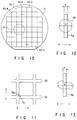
- FIG. 10 shows a semiconductor wafer.
- FIG. 11 presents an enlarged view of a region A encircled by a broken line in FIG. 10.
- an alignment mark XA for the alignment (positioning) of that chip area with a mask in the X direction
- an alignment mark YA for the alignment (positioning) of the chip area with the mask in the Y direction, for example.
- the two alignment marks XA and YA are formed as a pair on the dicing lines adjoining one chip area.
- a single alignment mark which permits the alignment both in the X and Y directions may be formed on the dicing line.
- the alignment marks XA and YA are provided to expose a resist to light to obtain a predetermined pattern in a photoetching step or the like.
- the size G of the grain 24 becomes 1 to 4 ⁇ m, so that the edge-to-edge width H of the alignment mark XA in the X direction is set to 1 ⁇ m or narrower. If the metal film is made of copper, the size G of the grain 24 becomes 4 to 5 ⁇ m, so that the edge-to-edge width H of the alignment mark XA in the X direction is set to 4 ⁇ m or narrower.
- the edge-to-edge width H of this alignment mark YA in the Y direction is also set smaller than the diameter G of the grain of the metal film on the alignment mark YA.
- FIG. 13 shows a semiconductor device according to a second embodiment of the present invention. This embodiment is applied to the case where the shape of the grain of the metal film formed on the alignment mark XA is not determined specifically.
- the edge-to-edge width H of the alignment mark YA in the Y direction is set smaller than the diameter G of the grain on the metal film on the alignment mark YA.
- the edge-to-edge width of the alignment mark XA in the X direction is set smaller than the average size, L, of the metal film.
- the edge-to-edge width of the alignment mark YA in the Y direction is set smaller than the average size L of the metal film.
- the average size L is defined as follows.
- the edge-to-edge width H of the alignment mark XA in the X direction is set smaller than the average size of the metal film.
- the edge-to-edge width H of the alignment mark YA in the Y direction is set smaller than the average size of the metal film.
- FIG. 20A shows a semiconductor device according to a fourth embodiment of the present invention.
- This alignment mark XYA has a square shape as viewed from above the semiconductor wafer.
- the alignment mark XYA may be a projection or a recess formed on the semiconductor wafer.
- a metal film (of aluminum, copper or the like) is formed on the alignment mark XYA.
- This alignment mark XYA is provided for the alignment of, for example, a single chip area in the X direction and Y direction.
- the edge-to-edge width, H1 of the alignment mark XYA in the X direction is set smaller than the width, XG, of a grain of the metal film on the alignment mark XYA (or the diameter if the grain is circular) or the average size L.
- the edge-to-edge width, H2, of the alignment mark XYA in the Y direction is set smaller than the width, YG, of a grain of the metal film on the alignment mark XYA (or the diameter if the grain is circular) or the average size L.
- FIG. 20B shows a semiconductor device according to a fifth embodiment of the present invention.
- This alignment mark XYA has an L shape (hook shape) as viewed from above the semiconductor wafer.
- the alignment mark XYA may be a projection or a recess formed on the semiconductor wafer.
- a metal film (of aluminum, copper or the like) is formed on the alignment mark XYA.
- This alignment mark XYA is provided for the alignment of, for example, a single chip area in the X direction and Y direction.
- the edge-to-edge width, H1 of the alignment mark XYA in the X direction is set smaller than the width, XG, of a grain of the metal film on the alignment mark XYA (or the diameter if the grain is circular) or the average size L.
- the edge-to-edge width, H2, of the alignment mark XYA in the Y direction is set smaller than the width, YG, of a grain of the metal film on the alignment mark XYA (or the diameter if the grain is circular) or the average size L.
- FIG. 16 shows a stepper that executes alignment through image processing.
- FIG. 17A shows an image recognizing area at the time the alignment mark is recognized by the stepper in FIG. 16.
- FIG. 17B shows a signal waveform obtained in the image recognizing area in FIG. 17A.
- the edge-to-edge width H of the alignment mark XA in the X direction is smaller than the X directional width of the grain on the metal film on the alignment mark XA (the diameter if the grain is circular) or the average size. It is therefore possible to prevent the grain of the metal film from making the detection of the recesses and projections of the metal film on the alignment mark difficult, and substantially the same recesses and projections as those of the alignment mark XA appear on the metal film.
- the stepper can accurately detect the edges of the alignment mark as indicated by the waveform chart in FIG. 17B.
- the alignment of a chip area on the semiconductor wafer with the mask can therefore be executed accurately by moving the stage.
- the size of the image recognizing area can be reduced to 1/5 of the conventionally required size.
- the number of grains on the metal film included in the image recognizing area becomes smaller than that of the prior art. Accordingly, it is difficult for noise to appear on the waveform shown in FIG. 17B, so that the edges of the alignment mark can be detected accurately without using approximation.
- the throughput of the semiconductor device can be improved.
- FIG. 18 shows a stepper that executes alignment using a laser.
- a semiconductor wafer 41 is placed on a stage 42.
- a laser tube 43 irradiates an He-Ne laser beam.
- This He-Ne laser beam is shaped into a slit-like beam and is then irradiated on the alignment mark XA on the semiconductor wafer 41.
- the He-Ne laser beam is diffracted and scattered by the step of the alignment mark.
- a detector 44 detects the diffracted light or scattered light.
- a signal processor 45 processes the output signal of the detector 44.
- a controller 46 recognizes the alignment mark based on a signal waveform obtained from the signal processor 45.
- a driver 47 executes alignment based on an instruction from the controller 46. After the alignment is completed, exposure (printing) is carried out using a reticule 48.
- FIG. 19A shows a laser scanning path at the time the stepper in FIG. 18 recognizes the alignment mark.
- FIG. 19B shows a signal waveform obtained by the laser scanning in FIG. 19A.
- the edge-to-edge width H of the alignment mark XA in the X direction is smaller than the X directional width of the grain on the metal film on the alignment mark XA (the diameter if the grain is circular) or the average size. It is therefore possible to prevent the grain of the metal film from making the detection of the recesses and projections of the metal film on the alignment mark difficult, and substantially the same recesses and projections as those of the alignment mark XA appear on the metal film.
- the position of the alignment mark can accurately be detected as indicated by the waveform chart in FIG. 19B.
- the alignment of a chip area on the semiconductor wafer with the mask can therefore be executed accurately by moving the stage.
- the spot size of the He-Ne laser image can be reduced to about a half.
- the scanning area of the laser beam can thus be reduced, so that the throughput of the semiconductor device can be improved.
- the spot size of the He-Ne laser image becomes about a half, the number of grains on the metal film included in the laser scanning area is reduced considerably. It therefore becomes difficult for noise to appear on the waveform shown in FIG. 19B, so that the threshold value of the slice circuit for removing the noise can be reduced to a half.
- FIGS. 21A through 21C illustrate how to perform alignment with the alignment mark of the present invention having a projection and pattern a metal film.
- a metal film is formed on the semiconductor substrate under given conditions. Thereafter, for example, the number of grains, n, on the metal film which are included in any given unit area S on the semiconductor substrate is obtained.
- the value that is obtained from the equation 2 ⁇ (S/n ⁇ ) 1/2 is taken as the average size L.
- the average size L may be obtained by other methods.
- the alignment mark XA is formed in such a way that, as viewed from above the semiconductor wafer 51, the X directional width of at least one projection becomes smaller than the average size obtained from the above equation, for example.
- an alignment mark for the alignment in the Y direction is formed in such a way that, as viewed from above the semiconductor wafer 51, the Y directional width of at least one projection becomes smaller than the average size obtained from the above equation, for example.
- the average size L generally becomes 1 to 4 ⁇ m, so that the X directional width of the alignment mark is set to 1 ⁇ m or narrower. If the metal film is made of copper, the average size L generally becomes 4 to 5 ⁇ m, so that the X directional width of the alignment mark XA is set to 4 ⁇ m or narrower.
- a metal film 52 is formed on the semiconductor substrate 51 under the aforementioned given conditions as shown in FIG. 21B. At this time, projections are also formed on the metal film 52 on the alignment mark XA. A resist film 53 is formed on the metal film 52.
- the semiconductor wafer 51 is moved on the stage of the stepper which executes alignment through image processing, for example.
- Light is irradiated on the metal film 52 on the alignment mark XA to detect the recesses and projections of this metal film 52.
- the X directional alignment of a chip area on the semiconductor wafer 51 with the mask is performed.
- the Y directional alignment of the chip area on the semiconductor wafer 51 with the mask is performed.
- exposure is performed on the resist film 53 to transfer the pattern on the mask onto the resist film 53.
- the resist film 53 is developed to form a predetermined pattern on the resist film 53.
- the metal film 52 is patterned with the resist film 53 as a mask.
- the alignment mark can easily be detected and the alignment of a chip area on the semiconductor wafer with the mask can accurately be carried out. It is therefore possible to reduce the alignment error between the chip area on the semiconductor wafer and the mask, thus ensuring the patterning of the metal film at high precision.
- FIGS. 22A through 22C illustrate how to perform alignment with the alignment mark of the present invention having a projection and pattern a metal film.
- a metal film is formed on the semiconductor substrate under given conditions. Thereafter, for example, the number of grains, n, on the metal film which are included in any given unit area S on the semiconductor substrate is obtained.
- the value that is obtained from the equation 2 ⁇ (S/n ⁇ ) 1/2 is taken as the average size L.
- the average size L may be obtained by other methods.
- an alignment mark XA which is constituted of at least one recess is formed on a semiconductor wafer (semiconductor substrate) 61.
- This alignment mark XA is provided for the alignment of a chip area on the semiconductor wafer 61 in the X direction.
- an alignment mark for the alignment of a chip area in the Y direction is formed.
- the alignment mark XA is formed in such a way that, as viewed from above the semiconductor wafer 61, the X directional width of at least one recess becomes smaller than the average size obtained from the above equation, for example.
- an alignment mark for the alignment in the Y direction is formed in such a way that, as viewed from above the semiconductor wafer 61, the Y directional width of at least one recess becomes smaller than the average size obtained from the above equation, for example.
- a metal film 62 is formed on the semiconductor substrate 61 under the aforementioned given conditions as shown in FIG. 22B. At this time, recesses are also formed on the metal film 62 on the alignment mark XA. A resist film 63 is formed on the metal film 62.
- the semiconductor wafer 61 is moved on the stage of the stepper which executes alignment through image processing, for example.
- Light is irradiated on the metal film 62 on the alignment mark XA to detect the recesses and projections of this metal film 62.
- the X directional alignment of a chip area on the semiconductor wafer 61 with the mask is performed.
- the Y directional alignment of the chip area on the semiconductor wafer 61 with the mask is performed.
- exposure is performed on the resist film 63 to transfer the pattern on the mask onto the resist film 63.
- the resist film 63 is developed to form a predetermined pattern on the resist film 63. Then, the metal film 62 is patterned with the resist film 63 as a mask.
- the alignment mark can easily be detected and the alignment of a chip area on the semiconductor wafer with the mask can accurately be carried out. It is therefore possible to reduce the alignment error between the chip area on the semiconductor wafer and the mask, thus ensuring the patterning of the metal film at high precision.
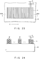
- FIG. 23 shows a semiconductor device according to a seventh embodiment of the present invention.
- FIG. 24 is a cross-sectional view taken along the line XXIV-XXIV' in FIG. 23.
- This alignment mark comprises recesses 12 and projections 13 formed on an insulating layer 11 on a semiconductor substrate 10.
- the recesses 12 and projections 13 are alternately arranged in a row on the semiconductor substrate 10.
- the alignment mark according to this embodiment differs from the conventional alignment marks in the following points.
- the size G of the grain becomes 1 to 4 ⁇ m, so that the edge-to-edge width H of the alignment mark XA in the X direction is set to 1 ⁇ m or narrower. If the metal film is made of copper, the size G of the grain becomes 4 to 5 ⁇ m, so that the edge-to-edge width H of the alignment mark XA in the X direction is set to 4 ⁇ m or narrower.
- the size of the grain on the metal film 14 varies with the conditions for the high-temperature sputtering method for forming this metal film or the conditions for processing this metal film by the laser melting method.
- the concept of the present invention is such that in performing the X directional alignment of a single chip area, the X directional width of the recesses or projections of the alignment mark is set smaller than the X directional width of the grain on the metal film on the alignment mark (diameter if the grain is circular) or the average size L, and in performing the Y directional alignment of a single chip area, the Y directional width of the recesses or projections of the alignment mark is set smaller than the Y directional width of the grain on the metal film on the alignment mark (diameter if the grain is circular) or the average size L.
- FIG. 25 shows a semiconductor device according to an eighth embodiment of the present invention.
- FIG. 26 is a cross-sectional view taken along the line XXVI-XXVI' in FIG. 25.
- This alignment mark comprises recesses 12 and projections 13 formed on an insulating layer 11 on a semiconductor substrate 10.
- the recesses 12 and projections 13 are alternately arranged in a row on the semiconductor substrate 10.
- the recesses 12 are constituted of slit-like holes formed in the insulating layer 11 formed on the semiconductor substrate 10.
- the alignment of this semiconductor device is executed by detecting the edges of the boundaries between the recesses 12 and projections 13 and recognizing the alignment mark.
- the alignment mark according to this embodiment differs from the conventional alignment marks in the following points.
- this alignment mark is for the X directional alignment
- the row of the recesses and projections are formed to extend in the X direction.
- the width H of the recesses 12 and projections 13 of the alignment mark in the row direction (X direction) is smaller than the X directional width of the grain on the metal film on the alignment mark (the diameter if the grain is circular) or the average size.
- the size G of the grain becomes 1 to 4 ⁇ m, so that the edge-to-edge width H of the alignment mark XA in the X direction is set to 1 ⁇ m or narrower. If the metal film is made of copper, the size G of the grain becomes 4 to 5 ⁇ m, so that the edge-to-edge width H of the alignment mark XA in the X direction is set to 4 ⁇ m or narrower.
- the width H of the recesses 12 and projections 13 of those alignment marks in the row direction (X direction) is about 6 ⁇ m regardless of the size of the grain on the metal film 14.
- the size of the grain on the metal film 14 varies with the conditions for the high-temperature sputtering method for forming this metal film or the conditions for processing this metal film by the laser melting method.
- the concept of the present invention is such that in performing the X directional alignment of a single chip area, the X directional width of the recesses or projections of the alignment mark is set smaller than the X directional width of the grain on the metal film on the alignment mark (diameter if the grain is circular) or the average size L, and in performing the Y directional alignment of a single chip area, the Y directional width of the recesses or projections of the alignment mark is set smaller than the Y directional width of the grain on the metal film on the alignment mark (diameter if the grain is circular) or the average size L.
- a grain is formed on the metal film 14 deposited on the semiconductor substrate 10.
- the X directional width of the recesses or projections of the alignment mark is set smaller than the X directional width of the grain on the metal film on the alignment mark (diameter if the grain is circular) or the average size.
- FIG. 29 shows an alignment signal waveform obtained by the stepper when the alignment of the semiconductor device in FIGS. 27 and 28 is executed through image processing.
- the alignment signal waveform has not been influenced by the grain on the metal film, and the high and low intensities of the signal waveform are regularly repeated.
- the stepper accurately detects the edges of the recesses and projections of the alignment mark. It is therefore possible to align the semiconductor device accurately, thus eliminating the misalignment-oriented problem at the time the metal film is processed.
- the alignment marks of the seventh and eighth embodiments can be used for the alignment which involves image processing and the alignment which uses a laser beam.
- the alignment mark according to this embodiment is the same as the conventional ones in that the alignment mark comprises recesses 12 and projections 13 formed on the insulating layer 11 on the semiconductor substrate 10.
- the alignment mark according to this embodiment however differs from the conventional ones in that the projections 13 have an annular shape as viewed from above the semiconductor substrate 10.
- the projection 13 is the projection 13 of the conventional alignment marks (see FIGS. 1 and 2) whose center portion is removed, leaving only the peripheral portion.
- the X directional width H of the projections 13 of this alignment mark is set smaller than the X directional width of the grain on the metal film on the alignment mark (diameter if the grain is circular) or the average size.
- the metal film 14 is formed by the high-temperature sputtering method or is processed by the laser melting method to be planarized.
- the alignment mark has a plurality of annular projections 13 arranged in a row in the X direction.
- the alignment of this semiconductor device is performed by detecting the edges of the boundaries between the recesses 12 and projections 13 to thereby detect the alignment mark.
- the alignment mark according to this embodiment has annular recesses 12 as viewed from above the semiconductor substrate 10.
- the X directional width H of the recesses 12 of this alignment mark is set smaller than the X directional width of the grain on the metal film on the alignment mark (diameter if the grain is circular) or the average size.
- the metal film 14 is formed by the high-temperature sputtering method or is processed by the laser melting method to be planarized.
- the alignment mark has a plurality of annular recesses 12 arranged in a row in the X direction.
- the alignment of this semiconductor device is performed by detecting the edges of the boundaries between the recesses 12 and projections 13 to thereby detect the alignment mark.
- FIG. 34 shows a semiconductor device having a metal film (planarized) deposited on the alignment mark according to the ninth embodiment.
- FIG. 35 is a cross-sectional view taken along the line XXXV-XXXV' in FIG. 34.
- FIG. 36 shows a semiconductor device having a metal film (planarized) deposited on the alignment mark according to the tenth embodiment.
- FIG. 37 is a cross-sectional view taken along the line XXXVII-XXXVII' in FIG. 36.
- a metal film 14 is deposited on the semiconductor substrate 10 while heating the semiconductor substrate 10 to 460°C or above by the high-temperature sputtering method, or after deposition on the semiconductor substrate 10 by sputtering, the metal film 14 is planarized by the laser melting method.
- a grain is formed on the metal film 14 deposited on the semiconductor substrate 10.
- the X directional width of the recesses or projections of the alignment mark is set smaller than the X directional width of the grain on the metal film on the alignment mark (diameter if the grain is circular) or the average size.
- the recesses or projections are annular and are arranged in a row in the X direction.
- FIG. 38 shows an alignment signal waveform obtained by the stepper when the alignment of the semiconductor device in FIGS. 34 and 35 is executed through image processing.
- the alignment signal waveform has not been influenced by the grain on the metal film, and the high and low intensities of the signal waveform are regularly repeated.
- the stepper accurately detects the edges of the recesses and projections of the alignment mark. It is therefore possible to align the semiconductor device accurately, thus eliminating the misalignment-oriented problem at the time the metal film is processed.
- the alignment marks of this embodiment can be used for the alignment which involves image processing and the alignment which uses a laser beam.
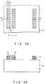
- FIG. 39 shows a semiconductor device according to an eleventh embodiment of the present invention.
- FIG. 40 is a cross-sectional view taken along the line XXXX-XXXX' in FIG. 39.
- the alignment of the semiconductor device is performed by detecting the recesses and projections of the metal film on the alignment mark to thereby detect the alignment mark.
- FIG. 41 shows a semiconductor device according to a twelfth embodiment of the present invention.
- FIG. 42 is a cross-sectional view taken along the line XXXX-XXXX' in FIG. 41.
- the alignment mark of this embodiment is the alignment mark of the eighth embodiment whose recesses 12 are constituted by a bit pattern or a group of square-shaped holes.
- the bit pattern of the recesses 12 is provided on the insulating layer 12 formed on the semiconductor substrate 10. This alignment mark is provided for the alignment of, for example, a single chip area in the X direction.
- the alignment of the semiconductor device is performed by detecting the recesses and projections of the metal film on the alignment mark to thereby detect the alignment mark.
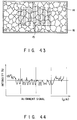
- FIG. 43 shows a metal film formed on an alignment mark.
- the feature of the eleventh and twelfth embodiments lie in that in performing the X directional alignment of, for example, a single chip area, the X directional width H of the bit pattern is set smaller than the width of a grain on the metal film formed on the alignment mark (or the diameter if the grain is circular) or the average size, as viewed from above the semiconductor substrate.
- FIG. 44 shows an alignment signal waveform obtained by the stepper when the alignment of the semiconductor device in FIG. 43 is executed through image processing.
- FIG. 45 illustrates the principle of the alignment of the eleventh and twelfth embodiments.
- the recesses or projections are formed by a bit pattern.
- an image recognizing area 17 contains a plurality of bit patterns. More specifically, the alignment signal waveform for that portion in the image recognizing area 17 which includes a bit pattern becomes as shown in (a) in FIG. 45 and the alignment signal waveform for that portion in the image recognizing area 17 which does not include a bit pattern becomes as shown in (b) in FIG. 45.
- the alignment signal waveform shown in FIG. 44 has not been influenced greatly by the grain on the metal film, and the high and low intensities of the signal waveform are regularly repeated. That is, the stepper can accurately detect the recesses and projections of the metal film on the alignment mark, thus ensuring high-precision alignment.
- the X directional width H of the recesses or projections of the alignment mark is set smaller than the X directional width of a grain on the metal film formed on the alignment mark (or the diameter if the grain is circular) or the average size, as viewed from above the semiconductor substrate.
- the Y directional width H of the recesses or projections of the alignment mark is set smaller than the Y directional width of a grain on the metal film formed on the alignment mark (or the diameter if the grain is circular) or the average size, as viewed from above the semiconductor substrate.
- this invention can contribute to improving the precision of alignment in the lithography technology.
Landscapes
- Physics & Mathematics (AREA)
- General Physics & Mathematics (AREA)
- Exposure And Positioning Against Photoresist Photosensitive Materials (AREA)
- Exposure Of Semiconductors, Excluding Electron Or Ion Beam Exposure (AREA)
Applications Claiming Priority (2)
| Application Number | Priority Date | Filing Date | Title |
|---|---|---|---|
| JP15043193 | 1993-06-22 | ||
| JP150431/93 | 1993-06-22 |
Publications (2)
| Publication Number | Publication Date |
|---|---|
| EP0631316A2 true EP0631316A2 (fr) | 1994-12-28 |
| EP0631316A3 EP0631316A3 (fr) | 1997-02-26 |
Family
ID=15496782
Family Applications (1)
| Application Number | Title | Priority Date | Filing Date |
|---|---|---|---|
| EP94109632A Withdrawn EP0631316A3 (fr) | 1993-06-22 | 1994-06-22 | Composant à semi-conducteur comprenant une marque d'alignement, procédé de fabrication dudit composant et méthode d'alignement. |
Country Status (2)
| Country | Link |
|---|---|
| EP (1) | EP0631316A3 (fr) |
| KR (1) | KR0139702B1 (fr) |
Cited By (1)
| Publication number | Priority date | Publication date | Assignee | Title |
|---|---|---|---|---|
| CN112408316A (zh) * | 2020-11-20 | 2021-02-26 | 中国科学院上海微系统与信息技术研究所 | 双面超表面结构的制备方法 |
Family Cites Families (7)
| Publication number | Priority date | Publication date | Assignee | Title |
|---|---|---|---|---|
| US4327292A (en) * | 1980-05-13 | 1982-04-27 | Hughes Aircraft Company | Alignment process using serial detection of repetitively patterned alignment marks |
| GB2109538A (en) * | 1981-11-02 | 1983-06-02 | Philips Electronic Associated | Electron beam alignment |
| JPS59232416A (ja) * | 1983-06-16 | 1984-12-27 | Oki Electric Ind Co Ltd | アライメントマ−ク |
| US4623403A (en) * | 1984-06-15 | 1986-11-18 | Texas Instruments Incorporated | Indexing of laser beam for programming VLSI devices |
| JP2723508B2 (ja) * | 1985-10-21 | 1998-03-09 | 日本電気株式会社 | 電子線直接描画のためのアライメント方法 |
| JPH0722179B2 (ja) * | 1985-12-27 | 1995-03-08 | 日本電気株式会社 | 半導体ウエ−ハの位置合せマ−クの形成方法 |
| JP2897248B2 (ja) * | 1989-04-18 | 1999-05-31 | 富士通株式会社 | 半導体装置の製造方法 |
-
1994
- 1994-06-22 KR KR1019940014237A patent/KR0139702B1/ko not_active Expired - Fee Related
- 1994-06-22 EP EP94109632A patent/EP0631316A3/fr not_active Withdrawn
Cited By (2)
| Publication number | Priority date | Publication date | Assignee | Title |
|---|---|---|---|---|
| CN112408316A (zh) * | 2020-11-20 | 2021-02-26 | 中国科学院上海微系统与信息技术研究所 | 双面超表面结构的制备方法 |
| CN112408316B (zh) * | 2020-11-20 | 2024-04-12 | 中国科学院上海微系统与信息技术研究所 | 双面超表面结构的制备方法 |
Also Published As
| Publication number | Publication date |
|---|---|
| KR0139702B1 (ko) | 1998-07-15 |
| EP0631316A3 (fr) | 1997-02-26 |
| KR950002014A (ko) | 1995-01-04 |
Similar Documents
| Publication | Publication Date | Title |
|---|---|---|
| US5786267A (en) | Method of making a semiconductor wafer with alignment marks | |
| US5017514A (en) | Method of manufacturing a semiconductor device using a main vernier pattern formed at a right angle to a subsidiary vernier pattern | |
| US5051807A (en) | Integrated semiconductor structure with incorporated alignment markings | |
| US5525840A (en) | Semiconductor device having an alignment mark | |
| US6670632B1 (en) | Reticle and method of fabricating semiconductor device | |
| KR100662833B1 (ko) | 반도체 기판, 반도체 장치의 제조 방법 및 반도체 장치의시험 방법 | |
| EP1162507A2 (fr) | Méthode d'alignement, méthode d'inspection d'erreurs de recouvrement, et photomasque | |
| US6255189B1 (en) | Method of manufacturing a semiconductor device in a silicon body, a surface of said silicon body being provided with an alignment grating and an at least partly recessed oxide pattern | |
| US5982044A (en) | Alignment pattern and algorithm for photolithographic alignment marks on semiconductor substrates | |
| US7944064B2 (en) | Semiconductor device having alignment post electrode and method of manufacturing the same | |
| JPH11345866A (ja) | 半導体デバイスおよび位置合せの方法 | |
| US7288848B2 (en) | Overlay mark for measuring and correcting alignment errors | |
| JP3970546B2 (ja) | 半導体装置及び半導体装置の製造方法 | |
| US6803668B2 (en) | Process-robust alignment mark structure for semiconductor wafers | |
| US20070023932A1 (en) | Wafer, reticle, and exposure method using the wafer and reticle | |
| US20040075179A1 (en) | Structural design of alignment mark | |
| EP0230648B1 (fr) | Procédé de formation de marques d'alignement dans un corps semi-conducteur | |
| EP0631316A2 (fr) | Composant à semi-conducteur comprenant une marque d'alignement, procédé de fabrication dudit composant et méthode d'alignement | |
| KR100610555B1 (ko) | 반도체소자 및 그 제조방법 | |
| US6468704B1 (en) | Method for improved photomask alignment after epitaxial process through 90° orientation change | |
| JP2840775B2 (ja) | 露光位置合せ方法 | |
| JP2005093461A (ja) | 半導体基板、半導体基板の製造方法および半導体装置の製造方法 | |
| JPH0555111A (ja) | 半導体装置の製造方法 | |
| CN120977994A (zh) | 半导体结构及其形成方法 | |
| US20050172256A1 (en) | Mask set for measuring an overlapping error and method of measuring an overlapping error using the same |
Legal Events
| Date | Code | Title | Description |
|---|---|---|---|
| PUAI | Public reference made under article 153(3) epc to a published international application that has entered the european phase |
Free format text: ORIGINAL CODE: 0009012 |
|
| 17P | Request for examination filed |
Effective date: 19940622 |
|
| AK | Designated contracting states |
Kind code of ref document: A2 Designated state(s): DE FR GB |
|
| PUAL | Search report despatched |
Free format text: ORIGINAL CODE: 0009013 |
|
| AK | Designated contracting states |
Kind code of ref document: A3 Designated state(s): DE FR GB |
|
| 17Q | First examination report despatched |
Effective date: 20070921 |
|
| STAA | Information on the status of an ep patent application or granted ep patent |
Free format text: STATUS: THE APPLICATION IS DEEMED TO BE WITHDRAWN |
|
| 18D | Application deemed to be withdrawn |
Effective date: 20080202 |