EP0631389B1 - Circuit de remise à zéro à la mise sous tension - Google Patents
Circuit de remise à zéro à la mise sous tension Download PDFInfo
- Publication number
- EP0631389B1 EP0631389B1 EP94401428A EP94401428A EP0631389B1 EP 0631389 B1 EP0631389 B1 EP 0631389B1 EP 94401428 A EP94401428 A EP 94401428A EP 94401428 A EP94401428 A EP 94401428A EP 0631389 B1 EP0631389 B1 EP 0631389B1
- Authority
- EP
- European Patent Office
- Prior art keywords
- inverter
- power
- node
- inverters
- power supply
- Prior art date
- Legal status (The legal status is an assumption and is not a legal conclusion. Google has not performed a legal analysis and makes no representation as to the accuracy of the status listed.)
- Expired - Lifetime
Links
Images



Classifications
-
- H—ELECTRICITY
- H03—ELECTRONIC CIRCUITRY
- H03K—PULSE TECHNIQUE
- H03K17/00—Electronic switching or gating, i.e. not by contact-making and –breaking
- H03K17/22—Modifications for ensuring a predetermined initial state when the supply voltage has been applied
-
- H—ELECTRICITY
- H03—ELECTRONIC CIRCUITRY
- H03K—PULSE TECHNIQUE
- H03K3/00—Circuits for generating electric pulses; Monostable, bistable or multistable circuits
- H03K3/02—Generators characterised by the type of circuit or by the means used for producing pulses
- H03K3/353—Generators characterised by the type of circuit or by the means used for producing pulses by the use, as active elements, of field-effect transistors with internal or external positive feedback
- H03K3/356—Bistable circuits
- H03K3/356008—Bistable circuits ensuring a predetermined initial state when the supply voltage has been applied; storing the actual state when the supply voltage fails
-
- H—ELECTRICITY
- H03—ELECTRONIC CIRCUITRY
- H03K—PULSE TECHNIQUE
- H03K3/00—Circuits for generating electric pulses; Monostable, bistable or multistable circuits
- H03K3/02—Generators characterised by the type of circuit or by the means used for producing pulses
- H03K3/353—Generators characterised by the type of circuit or by the means used for producing pulses by the use, as active elements, of field-effect transistors with internal or external positive feedback
- H03K3/356—Bistable circuits
- H03K3/3565—Bistables with hysteresis, e.g. Schmitt trigger
Definitions
- the present invention relates to a power-on reset circuit that generates a reset signal when a power is turned on and, more particularly, to a power-on reset circuit that generates a reset signal when a supply voltage has reached a certain threshold level.
- a power-on reset circuit having a constitution shown in Fig. 1 has been proposed as a type of the power-on reset circuit mentioned above.
- a resistor R1 and a capacitor C1 are connected to each other in series between Vcc power and ground.
- a node N1 a common connection point between the resistor R1 and the capacitor C1, is connected to an input terminal of an inverter 1.
- the inverter 1 is composed of a p-channel MOS (Metal Oxide Semiconductor) transistor Q1 and an n-channel MOS transistor Q2, both of which are connected to each other in series between power-supply voltage Vcc and ground, gates of the transistors being commonly connected to each other.
- MOS Metal Oxide Semiconductor
- a gate common connection point between the MOS transistors Q1 and Q2 provides an input terminal, which is connected to the node N1, while a node N2, which is a drain common connection point between the transistors, provides an output terminal from which a reset signal is outputted.
- the power-supply voltage Vcc goes up.
- a potential difference relative to the node N1 has exceeded a threshold voltage of the p-channel MOS transistor Q1
- the MOS transistor Q1 is turned on.
- a charging voltage of the capacitor C1 remains low.
- EP-A-0 150 480 and EP-A-0 421 124 describe power-up reset pulse generating circuits comprising cross-connected inverters.
- each inverter consists of a pair of transistors of opposite polarity connected in series between the power supply terminal and ground.
- US-A- 4 558 233, figure 3 discloses a power- on reset circuit with an inverter having a load, a transistor and a diode in series between a power supply node and a reference potential, the diode increasing the inverter threshold voltage.
- US- A- 4 013 902 discloses a power- on reset circuit with two cross- coupled inverters made up of a load resistor, a transistor and a diode in series, one diode being connected to a power supply node and the other diode being connected to ground.
- a power-on reset circuit comprising: a first power supply node; a reference potential node; a flip-flop composed of first and second cross-connected inverters, an output of the first inverter providing an input to the second inverter and an output of said second inverter providing an input to said first inverter; a series-connected circuit composed of a diode and a capacitor connected to each other in series between said first power supply node and said reference power supply node, a common connection point between said diode and said capacitor being connected to the output of one of the first and second inverters; and a reset signal generator for generating a reset signal based on a change in an output signal of one of the first and second inverters; characterised in that: each one of the first and second inverters comprises a load, a metal insulator semiconductor transistor and a diode connected in series between the first power supply node and the reference potential node, the load of the first inverter being connected to the first power supply no
- the power-on reset circuit wherein the above-mentioned flip-flop is composed of a pair of inverters whose load is made up of a high resistance element.
- the flip-flop has only one stable point when a supply voltage is sufficiently low and two stable points when the supply voltage is sufficiently high.
- This flip-flop recognises the state in which the supply voltage is high and the state in which the supply voltage is low.
- the reset signal is generated between the two states. In this set-up, the reset signal can be generated even if the supply voltage rises very slowly, thereby providing a stable reset-signal generation independently of how the power supply rises.
- the resistors used in the inverters constituting the flip-flop of this power-on reset circuit are made of high resistance elements, a leak current can be suppressed to a sufficiently low level.
- the driving transistors of the output-side inverter will not turn on when the supply voltage drops quickly to 0 V, thereby making it possible to generate the reset signal when the power voltage has risen again.
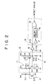
- FIG. 2 there is shown a circuit diagram of a power-on reset circuit practised as one preferred embodiment of the invention.
- a MOS Metal Oxide Semiconductor
- MIS Metal Insulator Semiconductor
- a resistor R11 as a load, a driving n-channel MOS transistor Q11, and a diode-connected n-channel MOS transistor Q12 are connected in series between Vcc power supply (a first power supply) and ground (a second power supply), thereby constituting an inverter 11.
- a diode-connected p-channel MOS transistor Q13, a driving P-channel MOS transistor Q14, and a resistor R12 as a load are connected in series between Vcc power supply and ground, thereby constituting an inverter 12.
- inverters 11 and 12 are cross-connected to each other to constitute a flip-flop 13. That is, a node N11, which is an output of the inverter 11, is connected to a gate of the driving p-channel MOS transistor Q14 of the inverter 12; a node N12, which is an output of the inverter 12, is connected to a gate of the driving n-channel MOS transistor Q11 of the inverter 11.
- values of the resistors R11 and R12 serving as loads for the inverters 11 and 12 are on the order of several giga ohms (G ⁇ )in order to suppress a leak current to a sufficiently low level (down to nano ampere (nA) level).
- a series-connected circuit 14 composed of a capacitor C11 and a diode-connected n-channel MOS transistor Q15.
- a common connection point of the series-connected circuit 14 is connected to one of outputs of the flip-flop 13, for example the node N11 of the inverter 11. It should be noted that a boundary between two stable states of the flip-flop 13 is determined by the values of the resistors R11 and R12 and subthreshold currents of MOS transistors Q11 through Q15.
- the reset pulse generator 16 comprises an inverter 17 for inverting a signal at a node N13, which is an output of the inverter 15, a delay circuit 18 for delaying the inverted signal coming from the inverter 17 for a predetermined period of time, and a NOR gate 19 in which the signal at the node N13 and the signal delayed by the delay circuit 18 are entered. Based on a difference between these signals, a reset pulse is generated. A width of the reset pulse is determined by the delay time of the delay circuit 18. For the delay circuit 18, a circuit having a constitution in which inverters are concatenated in an amount corresponding to the delay time.
- Vcc 0 V
- the potentials at the nodes N11 and N12 are both 0 V. If the power-supply voltage Vcc is sufficiently low, impedance of the MOS transistors Q11 through Q15 is sufficiently higher than that of the resistors R11 and R12, so that the flip-flop 13 has only one stable point. That is, the potential at the node N11 is fixed to Vcc level and the potential at the node N12 to ground level.
- the impedance of the MOS transistor Q13 and Q14 becomes generally equal to that of the resistor R12, causing the potential at the node N12 to shift from low level to high level.
- the inversion (shifting of the potential at the node N12 from low to high level) of the content of the flip-flop 13 is transmitted to the reset pulse generator 16 via the inverter 15. This causes the reset pulse generator 16 to generate a reset pulse.
- the signal at the node N13 is inverted by the inverter 17 and delayed by the delay circuit 18 by the predetermined period of time.
- the delayed signal is OR-ed with the signal at the node N13 to generate the reset pulse.
- the potential at the node N11 becomes a gate voltage at which a subthreshold current of the MOS transistor Q 12 becomes equal to a current flowing in the resistor R11 and the potential at the node N12 becomes a gate voltage at which a subthreshold current of the MOS transistor Q13 becomes equal to a current flowing in the resistor R12.
- a channel length of the MOS transistor Q15 is set long and a channel length of the MOS transistor Q 12 is set standard so that the subthreshold current of the MOS transistor Q12 becomes greater than that of the MOS transistor Q15.
- the MOS transistor Q15 is provided only as an external trigger for prompting the inversion of the flip-flop 13, thereby making an inverted state hard to revert again.
- the above-mentioned constitution allows the flip-flop 13 to recognize whether the power-supply voltage Vcc is in high state or low state and generate a reset pulse at a boundary in between, thereby securely providing reset pulse generation even if the power-supply voltage Vcc takes very long to rise.
- a variation in the potentials at the nodes N11 through N13 has a hysteresis and presents different hysteresis characteristics for rising and falling of the power-supply voltage Vcc.
- Fig. 4(A) to 4(C) there are shown variations of the potentials at the nodes N11 (A), N12 (B), and N13 (C) relative to the power-supply voltage Vcc.
- the reset pulse is generated when the potential at the node N13 shifts from high to low as described above.
- the potential at the node N11 becomes about -0.7 V (a drop by pn junction) due to the supply of a charge by the pn junction of drains of MOS transistors Q11 and Q14.
- the transistor Q14 will turn on if the potential at the node N11 is as low as about -0.7 V. Consequently, even in a low power-supply voltage state, the potential at the node N12 becomes Vcc level and the potential at the node N13 becomes ground level, thereby preventing the reset pulse from being generated.
- the diode-connected MOS transistor Q12 is connected to the MOS transistor Q11 in series and the diode-connected MOS transistor Q13 is connected to the MOS transistor Q14 in series, so that even when the power-supply voltage Vcc quickly drops to 0 V, the transistor Q14 will not turn on. Therefore, when the power-supply voltage Vcc rises again, the reset pulse can be generated securely.
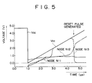
- FIG. 5 there are shown waveforms of the nodes N11, N12, and N13 obtained when the power-supply voltage Vcc has fallen temporarily and then risen again.
- the rush current to flow in the inverter 15 can be suppressed to a level lower than a current that flows in the resistor R12 by setting the threshold voltage of the p-channel MOS transistor constituting the inverter 15 to a level higher than the threshold voltage of the p-channel MOS transistor Q13 (for example, by setting a channel length of the transistor constituting the inverter 15 relatively long).
- a power-on reset circuit using a flip-flop composed of a pair of cross-connected inverters, wherein a common connection point between a diode and a capacitor connected to each other in series is connected to one output of the flip-flop to make the flip-flop recognize states in which a power supply voltage is high and low, thereby generating a reset signal at a boundary between the states.
- This novel setup surely generates the reset signal even when the power-supply voltage rises very slowly, thereby providing the stable generation of the reset signal without being affected by power-supply rising time.
- series connection of a diode to each of the driving transistors for the inverters constituting the flip-flop prevents the driving transistor of the output-side inverter from turning on, thereby ensuring the stable generation of the reset signal even when the power-supply voltage temporarily drops and then rises again.
Landscapes
- Electronic Switches (AREA)
Claims (13)
- Circuit de repositionnement à la mise sous tension, comprenant :caractérisé en ce que :un premier noeud d'alimentation électrique ;un noeud de potentiel de référence ;une bascule (13) composée de premier et deuxième inverseurs connectés en croix (11, 12), une sortie du premier inverseur (11) fournissant un signal d'entrée pour le deuxième inverseur (12) et une sortie du deuxième inverseur (12) fournissant un signal d'entrée pour le premier inverseur (11) ;un circuit série (14) constitué d'une diode (Q15) et d'un condensateur (C11) connectés l'un à l'autre en série entre ledit premier noeud d'alimentation électrique (Vcc) et ledit noeud de potentiel de référence, un point de connexion en commun entre ladite diode (Q15) et ledit condensateur (C11) étant connecté à la sortie (N11) de l'un des premier et deuxième inverseurs ; etun générateur de signal de repositionnement (16) servant à produire un signal de repositionnement sur la base d'une variation du signal de sortie de l'un des premier et deuxième inverseurs ;
chacun des premier et deuxième inverseurs (11, 12) comprend une charge (R11/R12), un transistor métal-isolant-semiconducteur (Q11/Q14) et une diode (Q12/Q13) connectés en série entre le premier noeud d'alimentation électrique et le noeud de potentiel de référence, la charge (R11) du premier inverseur (11) étant connectée au premier noeud d'alimentation électrique, la charge (R12) du deuxième inverseur (12) étant connectée au noeud de potentiel de référence, la diode (Q12) du premier inverseur (11) étant connectée au noeud de potentiel de référence, et la diode (Q13) du deuxième inverseur (12) étant connectée au premier noeud d'alimentation électrique. - Circuit de repositionnement à la mise sous tension selon la revendication 1, où, lorsque le potentiel du premier noeud d'alimentation électrique est différent de celui du noeud de potentiel de référence et est bas, l'impédance du transistor (Q11, Q14) et de la diode (Q12, Q13) de chacun desdits premier et deuxième inverseurs est suffisamment supérieure à celle de la charge (R11, R12) de chacun desdits premier et deuxième inverseurs pour que la bascule n'ait qu'un seul point stable, et, lorsque le potentiel du premier noeud d'alimentation électrique est suffisamment élevé pour amener le transistor du deuxième inverseur à devenir conducteur, la sortie de la bascule s'inverse.
- Circuit de repositionnement à la mise sous tension selon la revendication 1 ou 2, où les charges des premier et deuxième inverseurs sont des résistances (R11, R12).
- Circuit de repositionnement à la mise sous tension selon la revendication 1 ou 2, où les charges (R11, R12) des premier et deuxième inverseurs sont des éléments à résistance élevée.
- Circuit de repositionnement à la mise sous tension selon la revendication 3 ou 4, où les charges (R11, R12) des premier et deuxième inverseurs sont suffisamment grandes pour réduire le courant de fuite.
- Circuit de repositionnement à la mise sous tension selon l'une quelconque des revendications 1 à 5, où les premier et deuxième inverseurs (11, 12) comprennent respectivement un transistor métal-oxyde-semiconducteur de type n (Q11) et un transistor métal-oxyde-semiconducteur de type p (Q14).
- Circuit de repositionnement à la mise sous tension selon l'une quelconque des revendications 1 à 6, où la diode (Q12, Q13) de chacun desdits premier et deuxième inverseurs, connectée au transistor correspondant (Q11, Q14), est telle que, lorsque la tension (Vcc) du premier noeud d'alimentation électrique chute rapidement à 0 V, le transistor (Q11, Q14) correspondant ne passe pas dans l'état conducteur, si bien que, lorsque la première tension d'alimentation électrique (Vcc) s'élève de nouveau, l'impulsion de repositionnement est produite par ledit générateur d'impulsion de repositionnement (16).
- Circuit de repositionnement à la mise sous tension selon l'une quelconque des revendications 1 à 7, où la frontière entre deux états stables de la bascule (13) est déterminée par les valeurs des charges (R11, R12) des premier et deuxième inverseurs et les sous-courants de seuil des transistors (Q11, Q14) et des diodes (Q12, Q13) des premier et deuxième inverseurs ainsi que de la diode (Q15) du circuit série (14), ladite frontière correspondant au point où il est considéré que la tension (Vcc) du premier noeud d'alimentation électrique a commuté entre un état bas et un état haut.
- Circuit de repositionnement à la mise sous tension selon l'une quelconque des revendications 1 à 8, où les diodes (Q12, Q13) des premier et deuxième inverseurs sont des transistors connectés en diodes.
- Circuit de repositionnement à la mise sous tension selon l'une quelconque des revendications 1 à 9, où ledit générateur d'impulsion de repositionnement (16) est connecté à la sortie du deuxième inverseur (12) via un troisième inverseur (15), et un condensateur (C12) est connecté entre ledit noeud de potentiel de référence et une entrée dudit troisième inverseur (15).
- Circuit de repositionnement à la mise sous tension selon l'une quelconque des revendications 1 à 9, où ledit générateur d'impulsion de repositionnement (16) comprend un quatrième inverseur (17) servant à inverser le signal de sortie d'un troisième inverseur (15) connecté à ladite bascule (13), un circuit retardateur (18) servant à retarder, pendant une durée prédéterminée, un signal inversé venant du quatrième inverseur (17), et une porte NI (19) servant à produire une impulsion de repositionnement sur la base du signal de sortie dudit troisième inverseur (17) et du signal de sortie du circuit retardateur (18).
- Circuit de repositionnement à la mise sous tension selon la revendication 11, où la largeur de l'impulsion de repositionnement produite par ledit générateur d'impulsion de repositionnement (16) est déterminée par le temps de retard du circuit retardateur (18).
- Circuit de repositionnement à la mise sous tension selon l'une quelconque des revendications 1 à 12, où un premier noeud (N11) est prévu au niveau d'une connexion en commun entre la charge (R11) et le transistor (Q11) du premier inverseur (11), et un deuxième noeud (N12) est prévu au niveau d'une connexion en commun entre la charge (R12) et le transistor (Q14) du deuxième inverseur (12), de sorte que, lorsque le potentiel (Vcc) du premier noeud d'alimentation électrique est 0 V, le potentiel de chacun des premier et deuxième noeuds (N11 et N12) est 0V, et, lorsque le potentiel (Vcc) du premier noeud d'alimentation électrique est proche d'une valeur de seuil du deuxième inverseur (12), l'impédance du transistor (Q14) et de la diode (Q13) du deuxième inverseur (12) devient approximativement égale à celle de la charge (R12) du deuxième inverseur (12), ce qui amène le potentiel présent sur ledit deuxième noeud (N12) à passer d'un niveau bas à un niveau haut.
Applications Claiming Priority (3)
| Application Number | Priority Date | Filing Date | Title |
|---|---|---|---|
| JP17976193 | 1993-06-25 | ||
| JP179761/93 | 1993-06-25 | ||
| JP17976193A JP3277410B2 (ja) | 1993-06-25 | 1993-06-25 | パワーオンリセット回路 |
Publications (3)
| Publication Number | Publication Date |
|---|---|
| EP0631389A2 EP0631389A2 (fr) | 1994-12-28 |
| EP0631389A3 EP0631389A3 (fr) | 1995-08-30 |
| EP0631389B1 true EP0631389B1 (fr) | 1999-09-01 |
Family
ID=16071427
Family Applications (1)
| Application Number | Title | Priority Date | Filing Date |
|---|---|---|---|
| EP94401428A Expired - Lifetime EP0631389B1 (fr) | 1993-06-25 | 1994-06-24 | Circuit de remise à zéro à la mise sous tension |
Country Status (5)
| Country | Link |
|---|---|
| US (1) | US5517144A (fr) |
| EP (1) | EP0631389B1 (fr) |
| JP (1) | JP3277410B2 (fr) |
| KR (1) | KR100325025B1 (fr) |
| DE (1) | DE69420326T2 (fr) |
Families Citing this family (25)
| Publication number | Priority date | Publication date | Assignee | Title |
|---|---|---|---|---|
| US5821787A (en) * | 1994-10-05 | 1998-10-13 | Altera Corporation | Power-on reset circuit with well-defined reassertion voltage |
| US5703510A (en) * | 1996-02-28 | 1997-12-30 | Mitsubishi Denki Kabushiki Kaisha | Power on reset circuit for generating reset signal at power on |
| DE19742389A1 (de) * | 1997-09-25 | 1998-12-10 | Siemens Ag | Schaltung zur Erzeugung eines das Einschalten einer Versorgungsspannung signalisierenden Reset-Signals |
| US5917255A (en) * | 1998-01-20 | 1999-06-29 | Vlsi Technology, Inc. | Power-on-reset circuit having reduced size charging capacitor |
| US6052006A (en) * | 1998-05-27 | 2000-04-18 | Advanced Micro Devices, Inc. | Current mirror triggered power-on-reset circuit |
| JP2000181581A (ja) * | 1998-12-11 | 2000-06-30 | Nec Corp | 電源投入回路及びリセット方法 |
| KR100333666B1 (ko) * | 1999-06-30 | 2002-04-24 | 박종섭 | 다양한 파워-온 신호에 대하여 리셋신호를 생성하는 파워-온리셋회로 |
| US6288584B1 (en) * | 2000-10-05 | 2001-09-11 | Pericom Semiconductor Corp. | Zero standby-current power-on reset circuit with Schmidt trigger sensing |
| US6566919B2 (en) * | 2000-11-29 | 2003-05-20 | Silicon Storage Technology, Inc. | Power on circuit for generating reset signal |
| KR100427034B1 (ko) * | 2002-07-22 | 2004-04-14 | 주식회사 하이닉스반도체 | 반도체 장치의 피워온리셋 회로 |
| JP2005039635A (ja) | 2003-07-16 | 2005-02-10 | Matsushita Electric Ind Co Ltd | パワーオンリセット回路 |
| DE102004006254A1 (de) * | 2004-02-09 | 2005-09-01 | Infineon Technologies Ag | Schaltungsanordnung zur Erzeugung eines Rücksetzsignals nach einem Absinken und Wiederansteigen einer Versorgungsspannung |
| US7142478B2 (en) * | 2004-03-19 | 2006-11-28 | Infineon Technologies Ag | Clock stop detector |
| KR100614645B1 (ko) * | 2004-06-03 | 2006-08-22 | 삼성전자주식회사 | 파워-온 리셋회로 |
| JP4660160B2 (ja) * | 2004-10-28 | 2011-03-30 | Okiセミコンダクタ株式会社 | リセット回路 |
| KR20060071628A (ko) * | 2004-12-22 | 2006-06-27 | 주식회사 포스코 | 활성탄소섬유의 질소함량 증대방법 |
| JP2007058940A (ja) * | 2005-08-22 | 2007-03-08 | Sony Corp | 記憶装置、ファイル記憶装置、およびコンピュータシステム |
| US7661554B2 (en) * | 2005-12-13 | 2010-02-16 | Kimberly-Clark Worldwide, Inc. | Tissue sheet dispenser and process for making same |
| US8963590B2 (en) * | 2007-06-13 | 2015-02-24 | Honeywell International Inc. | Power cycling power on reset circuit for fuse initialization circuitry |
| US20080309384A1 (en) * | 2007-06-13 | 2008-12-18 | Honeywell International Inc. | Initialization Circuitry Having Fuse Leakage Current Tolerance |
| JP5476104B2 (ja) * | 2009-11-30 | 2014-04-23 | セイコーNpc株式会社 | パワーオンクリア回路 |
| US8536907B2 (en) * | 2011-09-24 | 2013-09-17 | Issc Technologies Corp. | Power on reset signal generating apparatus and method |
| JP6487882B2 (ja) * | 2016-08-12 | 2019-03-20 | ミネベアミツミ株式会社 | アドレス制御回路及びアドレス制御回路の制御方法 |
| CN112671392A (zh) * | 2020-12-24 | 2021-04-16 | 中国人民解放军国防科技大学 | 一种用于高电平复位电路的抗单粒子瞬态缓冲器 |
| CN115118261B (zh) * | 2022-07-11 | 2024-04-05 | 北京泽声科技有限公司 | 上电复位电路 |
Citations (4)
| Publication number | Priority date | Publication date | Assignee | Title |
|---|---|---|---|---|
| US4013902A (en) * | 1975-08-06 | 1977-03-22 | Honeywell Inc. | Initial reset signal generator and low voltage detector |
| EP0150480A2 (fr) * | 1984-01-16 | 1985-08-07 | Itt Industries, Inc. | Générateur d'impulsion pour l'établissement de l'état initial à l'enclenchement du secteur |
| US4558233A (en) * | 1982-02-16 | 1985-12-10 | Fujitsu Limited | CMOS power-on reset pulse generating circuit with extended reset pulse duration |
| EP0421124A2 (fr) * | 1989-10-02 | 1991-04-10 | Texas Instruments Incorporated | Circuit générateur d'impulsion à la mise sous tension |
Family Cites Families (14)
| Publication number | Priority date | Publication date | Assignee | Title |
|---|---|---|---|---|
| US3061942A (en) * | 1958-12-30 | 1962-11-06 | Philco Corp | Fabric dryer with lint burning means |
| NL6501840A (fr) * | 1965-02-13 | 1966-08-15 | ||
| US3508081A (en) * | 1966-08-17 | 1970-04-21 | Honeywell Inc | Circuit arrangement for supplying a current signal to one or two loads |
| DE1908115A1 (de) * | 1969-02-19 | 1970-09-10 | Bosch Gmbh Robert | Schaltungsanordnung nach Art einer bistabilen Kippschaltung |
| DE2433328A1 (de) * | 1974-07-11 | 1976-01-29 | Philips Patentverwaltung | Integrierte schaltungsanordnung |
| US4169233A (en) * | 1978-02-24 | 1979-09-25 | Rockwell International Corporation | High performance CMOS sense amplifier |
| JPS60189029A (ja) * | 1984-03-08 | 1985-09-26 | Rohm Co Ltd | 電源オンリセツト回路 |
| GB8518692D0 (en) * | 1985-07-24 | 1985-08-29 | Gen Electric Co Plc | Power-on reset circuit arrangements |
| US4837458A (en) * | 1986-08-22 | 1989-06-06 | Hitachi, Ltd. | Flip-flop circuit |
| JP2741022B2 (ja) * | 1987-04-01 | 1998-04-15 | 三菱電機株式会社 | パワーオンリセツトパルス発生回路 |
| JP2680592B2 (ja) * | 1988-02-18 | 1997-11-19 | 三洋電機株式会社 | パワーオンリセット回路 |
| DE68905658T2 (de) * | 1988-05-16 | 1993-10-07 | Philips Nv | Schaltung zum Erzeugen eines impulsförmigen Signals. |
| US5113098A (en) * | 1991-03-29 | 1992-05-12 | Advanced Micro Devices, Inc. | Glitch remover circuit for transmission links |
| US5311070A (en) * | 1992-06-26 | 1994-05-10 | Harris Corporation | Seu-immune latch for gate array, standard cell, and other asic applications |
-
1993
- 1993-06-25 JP JP17976193A patent/JP3277410B2/ja not_active Expired - Fee Related
-
1994
- 1994-06-09 US US08/257,145 patent/US5517144A/en not_active Expired - Fee Related
- 1994-06-14 KR KR1019940013401A patent/KR100325025B1/ko not_active Expired - Fee Related
- 1994-06-24 DE DE69420326T patent/DE69420326T2/de not_active Expired - Fee Related
- 1994-06-24 EP EP94401428A patent/EP0631389B1/fr not_active Expired - Lifetime
Patent Citations (4)
| Publication number | Priority date | Publication date | Assignee | Title |
|---|---|---|---|---|
| US4013902A (en) * | 1975-08-06 | 1977-03-22 | Honeywell Inc. | Initial reset signal generator and low voltage detector |
| US4558233A (en) * | 1982-02-16 | 1985-12-10 | Fujitsu Limited | CMOS power-on reset pulse generating circuit with extended reset pulse duration |
| EP0150480A2 (fr) * | 1984-01-16 | 1985-08-07 | Itt Industries, Inc. | Générateur d'impulsion pour l'établissement de l'état initial à l'enclenchement du secteur |
| EP0421124A2 (fr) * | 1989-10-02 | 1991-04-10 | Texas Instruments Incorporated | Circuit générateur d'impulsion à la mise sous tension |
Also Published As
| Publication number | Publication date |
|---|---|
| DE69420326D1 (de) | 1999-10-07 |
| JP3277410B2 (ja) | 2002-04-22 |
| JPH0715308A (ja) | 1995-01-17 |
| DE69420326T2 (de) | 2000-03-02 |
| EP0631389A2 (fr) | 1994-12-28 |
| EP0631389A3 (fr) | 1995-08-30 |
| US5517144A (en) | 1996-05-14 |
| KR950002225A (ko) | 1995-01-04 |
| KR100325025B1 (ko) | 2002-06-20 |
Similar Documents
| Publication | Publication Date | Title |
|---|---|---|
| US5517144A (en) | Power-on reset circuit | |
| US5144159A (en) | Power-on-reset (POR) circuit having power supply rise time independence | |
| US4518873A (en) | Buffer circuit for driving a C-MOS inverter | |
| KR960004573B1 (ko) | 기동회로를 갖는 기준전압발생회로 | |
| US6249169B1 (en) | Transistor output circuit | |
| KR0132641B1 (ko) | 기판 바이어스 회로 | |
| US7248075B2 (en) | Level shifter with low leakage current | |
| US20050134355A1 (en) | Level shift circuit | |
| EP1608067A2 (fr) | Circuit d'initialisation | |
| EP0497319B1 (fr) | Dispositif de circuit intégré à semi-conducteur à circuit détecteur de potentiel de substrat | |
| US20030001554A1 (en) | Internal power voltage generator | |
| US4719367A (en) | Schmitt trigger circuit | |
| US5705946A (en) | Low power low voltage level shifter | |
| JPS58123223A (ja) | Mosパワ−オンリセツト回路 | |
| US6414529B1 (en) | Latch and D-type flip-flop | |
| KR960003087A (ko) | 수정발진회로 | |
| US5905399A (en) | CMOS integrated circuit regulator for reducing power supply noise | |
| JPH02228813A (ja) | バイポーラ・mos論理回路および半導体集積回路 | |
| KR102845796B1 (ko) | 지연 회로 | |
| EP0342735B1 (fr) | Circuit conçu pour engendrer un signal en forme d'impulsion | |
| EP0435335A1 (fr) | Circuit de transistor et circuit convertisseur de niveau | |
| JP3757518B2 (ja) | パワーオン・リセット回路 | |
| US5841306A (en) | Pulse generator for generating output pulse of a predetermined width | |
| KR100349356B1 (ko) | 파워 온 리셋 회로 | |
| US5319262A (en) | Low power TTL/CMOS receiver circuit |
Legal Events
| Date | Code | Title | Description |
|---|---|---|---|
| PUAI | Public reference made under article 153(3) epc to a published international application that has entered the european phase |
Free format text: ORIGINAL CODE: 0009012 |
|
| AK | Designated contracting states |
Kind code of ref document: A2 Designated state(s): DE FR GB |
|
| PUAL | Search report despatched |
Free format text: ORIGINAL CODE: 0009013 |
|
| AK | Designated contracting states |
Kind code of ref document: A3 Designated state(s): DE FR GB |
|
| 17P | Request for examination filed |
Effective date: 19960207 |
|
| 17Q | First examination report despatched |
Effective date: 19961213 |
|
| GRAG | Despatch of communication of intention to grant |
Free format text: ORIGINAL CODE: EPIDOS AGRA |
|
| GRAG | Despatch of communication of intention to grant |
Free format text: ORIGINAL CODE: EPIDOS AGRA |
|
| GRAH | Despatch of communication of intention to grant a patent |
Free format text: ORIGINAL CODE: EPIDOS IGRA |
|
| GRAH | Despatch of communication of intention to grant a patent |
Free format text: ORIGINAL CODE: EPIDOS IGRA |
|
| GRAA | (expected) grant |
Free format text: ORIGINAL CODE: 0009210 |
|
| AK | Designated contracting states |
Kind code of ref document: B1 Designated state(s): DE FR GB |
|
| REF | Corresponds to: |
Ref document number: 69420326 Country of ref document: DE Date of ref document: 19991007 |
|
| ET | Fr: translation filed | ||
| PLBE | No opposition filed within time limit |
Free format text: ORIGINAL CODE: 0009261 |
|
| STAA | Information on the status of an ep patent application or granted ep patent |
Free format text: STATUS: NO OPPOSITION FILED WITHIN TIME LIMIT |
|
| 26N | No opposition filed | ||
| PGFP | Annual fee paid to national office [announced via postgrant information from national office to epo] |
Ref country code: FR Payment date: 20010611 Year of fee payment: 8 |
|
| PGFP | Annual fee paid to national office [announced via postgrant information from national office to epo] |
Ref country code: DE Payment date: 20010618 Year of fee payment: 8 |
|
| PGFP | Annual fee paid to national office [announced via postgrant information from national office to epo] |
Ref country code: GB Payment date: 20010620 Year of fee payment: 8 |
|
| REG | Reference to a national code |
Ref country code: GB Ref legal event code: IF02 |
|
| PG25 | Lapsed in a contracting state [announced via postgrant information from national office to epo] |
Ref country code: GB Free format text: LAPSE BECAUSE OF NON-PAYMENT OF DUE FEES Effective date: 20020624 |
|
| PG25 | Lapsed in a contracting state [announced via postgrant information from national office to epo] |
Ref country code: DE Free format text: LAPSE BECAUSE OF NON-PAYMENT OF DUE FEES Effective date: 20030101 |
|
| GBPC | Gb: european patent ceased through non-payment of renewal fee |
Effective date: 20020624 |
|
| PG25 | Lapsed in a contracting state [announced via postgrant information from national office to epo] |
Ref country code: FR Free format text: LAPSE BECAUSE OF NON-PAYMENT OF DUE FEES Effective date: 20030228 |
|
| REG | Reference to a national code |
Ref country code: FR Ref legal event code: ST |