EP0632383A2 - Interface balayable pour microprocesseur non-balayable - Google Patents
Interface balayable pour microprocesseur non-balayable Download PDFInfo
- Publication number
- EP0632383A2 EP0632383A2 EP94304465A EP94304465A EP0632383A2 EP 0632383 A2 EP0632383 A2 EP 0632383A2 EP 94304465 A EP94304465 A EP 94304465A EP 94304465 A EP94304465 A EP 94304465A EP 0632383 A2 EP0632383 A2 EP 0632383A2
- Authority
- EP
- European Patent Office
- Prior art keywords
- processor
- scannable
- bus
- state
- circuit
- Prior art date
- Legal status (The legal status is an assumption and is not a legal conclusion. Google has not performed a legal analysis and makes no representation as to the accuracy of the status listed.)
- Ceased
Links
Images


Classifications
-
- G—PHYSICS
- G06—COMPUTING OR CALCULATING; COUNTING
- G06F—ELECTRIC DIGITAL DATA PROCESSING
- G06F11/00—Error detection; Error correction; Monitoring
- G06F11/22—Detection or location of defective computer hardware by testing during standby operation or during idle time, e.g. start-up testing
-
- G—PHYSICS
- G06—COMPUTING OR CALCULATING; COUNTING
- G06F—ELECTRIC DIGITAL DATA PROCESSING
- G06F11/00—Error detection; Error correction; Monitoring
- G06F11/22—Detection or location of defective computer hardware by testing during standby operation or during idle time, e.g. start-up testing
- G06F11/2205—Detection or location of defective computer hardware by testing during standby operation or during idle time, e.g. start-up testing using arrangements specific to the hardware being tested
- G06F11/2236—Detection or location of defective computer hardware by testing during standby operation or during idle time, e.g. start-up testing using arrangements specific to the hardware being tested to test CPU or processors
Definitions
- the present invention relates to the field of digital processing systems with diagnostic capabilities. More specifically, in one embodiment, the invention provides a means for scanning scannable processor circuitry without disturbing a non-scannable microprocessor which forms part of a digital system.
- a diagnostic system need only control the overall inputs to the circuit, and record the outputs.
- the outputs for a known set of inputs, when compared to an expected set of outputs, will indicate if the circuit is working properly.
- Circuits with memory elements, such as flip-flops, latches, and memory storage cells, are more complicated to diagnose.
- the internally remembered states must be known and controllable.
- Some internal states can be controlled by manipulation of the inputs to the circuit. For example, the internal state of a counter, i.e., its count, can be controlled by asserting a reset input of the counter to reach a known state, then clocking the clock input to reach the desired internal state. This, of course, is not practical with today's complex circuits. Furthermore, for certain tests, the internal state might need to be set to a state which is not reachable through mere manipulation of the circuit's inputs.
- a scan path is a serial path linking all the memory elements of a circuit, or at least those which are to be scannable elements into a serial stream. Placing the elements in a serial scan path allows the internal state to be read serially from one pin, and allows the internal state to be set with one pin.
- the integrated circuit has a mechanism for switching from a normal circuit operation mode to a test mode.
- a memory element In the normal circuit operation mode, a memory element is responsive to its inputs, and in a test mode, the memory element is responsive to data passing along the scan path. Consequently, shifting data into and out of the scan path will cause the outputs of the memory element to change as the data shifts by. If the memory element is one which directly affects the output of the circuit, the shifting of test data on the scan path will appear as data rippling over the outputs of the circuit.
- scan in To set the circuit to a known state (scan in), settings for each memory element in the scan path are scanned into a scan input, and to read the state of the circuit (scan out), data is read from a scan path output.
- the scan in and scan out is performed by clocking the scan path by a number of clocks equal to the number of memory elements in the scan path.
- a scan enable must be provided, which when not asserted allows for normal operation of the circuit.
- the circuit behaves as designed, and when the scan enable is asserted, the circuit behaves as a serial register encompassing all the diagnosable memory elements.
- Fig. 1 illustrates this concept.
- Fig. 1 shows a parallel register 10, with 8 bits of data input, 8 bits of data output, a clock input, an input for a scan enable signal, a scan data input, and a scan data.
- Register 10 operates as a register when the scan enable signal is not asserted, with data passing from the inputs I0-I7 to the outputs O0-O7 with the clock.
- register 10 contains all zeros, and "10000000" is to be scanned in, where the "1" is to end up as bit 7. Because the scan input is coupled to bit 0, the "1" will ripple through each of the outputs as it is being clocked in, thus disturbing any circuit element which depends on the output of register 10, thereby disturbing the states of other circuits.
- Another solution is to coordinate the scan of register 10 with the scan of the dependent elements.
- the dependent elements are not scannable, such as where the dependent element is an enclosed IC provided by another manufacturer, this solution is not possible.
- An improved circuit diagnostic system is provided by the present invention.
- the diagnostic system can scan everything up to the boundary of a non-scannable circuit element, without disturbing the non-scannable element.
- One such diagnostic system for a digital computer is a processor board comprising scannable processor ASIC's (Application Specific Integrated Circuits), including a processor interface chip (PIC), which interfaces a non-scannable microprocessor and the other scannable processor ASIC's with a processor bus between the microprocessor and the PIC.
- a scan controller is provided which reads and writes scan data through the scannable ASIC's, including the PIC.
- the ASIC's are typically individual chips on a processor board, with each chip having a separately controllable scan path. However, in alternate embodiments, more than one ASIC might be combined on a single chip, or more than one chip might make up a single ASIC. Also, the processor circuitry need not be on a single board.
- the scan controller is itself an ASIC, a Maintenance and Diagnostic Clip (MDC), which makes requests of the PIC to bus-step the microprocessor.
- MDC Maintenance and Diagnostic Clip
- the microprocessor and the processor ASIC's run normally, until the PIC determines that the microprocessor can be held up and that the PIC can be scanned without violating the bus protocol. At that point, the microprocessor is held up, waiting for a response from the PIC. Because the microprocessor is expecting the wait, a delay in getting the response will not necessarily affect the state of the microprocessor.
- One advantage of the present invention is that the processor board, up to the processor bus, can be scanned without disturbing the state of the microprocessor. This is useful where a computer system including a non-scannable microprocessor needs to be tested, set into a known state, or debugged in a setting closely aligned with a normal operation setting.
- Another advantage of the present invention is that it also allows for the processor board to be bus-stepped without requiring any special hardware in the microprocessor. If no special hardware is needed, then a standard microprocessor chip could be used.
- Yet another advantage of the present invention is that it allows for clock cycle single-stepping of the scannable ASIC's without the microprocessor interfering with the test. Some diagnostics can be run even without the presence of the microprocessor.
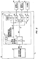
- Fig. 2 is a block diagram of a digital computer system 20 with a non-scannable microprocessor 22 and scannable processor circuitry 24 on a processor board 21.
- Processor circuitry 24 includes a variety of ASIC's such as a processor interface chip (PIC) 30, a memory interface chip (MIC) 32, interprocessor bus controllers 34x,y (IPBX/IPBY), input/output controller system (IOS) 36 and a maintenance and diagnostic chip (MDC) 38.
- PIC processor interface chip
- MIC memory interface chip
- IOS input/output controller system
- MDC maintenance and diagnostic chip
- Processor circuitry 24 is interconnected by three busses, an internal bus (IBus) 40, a maintenance bus (Mbus) 42, and an external bus (EBus) 43.
- IBus internal bus
- Mbus maintenance bus
- EBus external bus
- PIC 30 includes state machines, shown in more detail in Fig. 5, whose operation is discussed in connection with Figs. 3 and 5.
- the Mbus contains signal lines for controlling the scan of the ASIC's attached to the Mbus, allowing the MDC to set up an ASIC for a scan operation, or to hold its state in place. Holding the state of one ASIC in place allows the MDC to scan another ASIC without disturbing the state of the held ASIC.
- the Mbus also contains scan data lines used for writing scan data into an ASIC and for reading scan data out of an ASIC.
- the MDC interfaces with the PIC over three lines, DIAG_REQ, STEP_REQ, and DIAG_OK, although in some embodiments, the information provided by these signals is distributed over a different set of signal lines.
- Microprocessor 22 issues requests to the PIC over a processor bus (PBus) 50, which in turn relays the requests over the IBus to other ASIC's. For example, if microprocessor 22 requests a memory write, the request will include the data to be written and will be passed from the PIC to the MIC for storage of the data accompanying the request into memory 44. Similarly, a read request for a given block of memory 44 is sent from microprocessor 22 over the PBus to the PIC, and then from there to the MIC over IBus 40. In response, the MIC retrieves the data from memory 44 and passes it to the PIC, which relays it to microprocessor 22 at the appropriate time in the PBus protocol.
- PBus processor bus
- the MDC can control the ASIC's over the Mbus.
- the Mbus is shown leading to each ASIC individually, in some embodiments, the scan path through the ASIC's is serial, i.e., all the scan data runs through each ASIC. The latter configuration is useful where a connection between two ASIC's is less costly than the connections from each ASIC to the MDC.
- One means for controlling diagnostics of an ASIC is by scanning a desired state into the ASIC, over the Mbus. Because each ASIC within processor circuitry 24 is scannable, the state of the ASIC can be monitored and changed. Therefore, the MDC need not be concerned with the internal operation of the ASIC's interacting on the IBus since the states of all scannable ASIC's can be scanned in or held. For example, during a scan operation, the MIC can be scanned in such a way that the rippling of the scan bits appears on the IBus, but this is not a problem if each ASIC on the IBus is also under the control of the MDC.
- the ability of the inputs to the ASIC to affect the state of the circuitry inside the ASIC is blocked.
- the MDC can issue a hold command over the Mbus to all ASIC's which are not being scanned, to prevent the rippling on the IBus from triggering an undesirable input to the unscanned as IC's.
- the Mbus is all that is needed between the MDC and that ASIC.
- PIC 30 which has an interface to microprocessor 22, which is not controllable by MDC 38.
- the PIC is freely scannable by the MDC without regard to the status of the PBus, except for memory elements which would affect the signals put out on the PBus, but even those memory elements are scannable when provided with the control logic embodied in the state diagram shown in Fig. 3.
- These signals comprise M address/data lines and K control lines for a total of N lines.
- microprocessor 22 When certain conditions are met, microprocessor 22 will not be affected by the signals on the address/data lines. These conditions are met when control signals passed from the PIC to the microprocessor indicate that the data on the address/data lines is not valid.
- microprocessor 22 is waiting for a response to a microprocessor request and a "response ready" signal from the PIC to the microprocessor has not yet been asserted by the PIC.
- the MDC must assure that the PBus is in a condition such that a scan can occur without causing undesired operation of microprocessor 22.
- Fig. 3 is a state diagram showing the various protocol states between the MDC and the PIC.
- the state is tracked by a state machine 52 (see Fig. 5) within the PIC, although other configurations are possible. Significantly, even this state machine 52 is scannable.
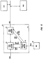
- Fig. 5 shows PIC 30 in greater detail.
- PIC includes state machines 52, 54, 56. Signal connections are provided for state machine 52 to send a stay_off_PBus signal to PBus state machine 54 and a stay_off_IBus signal to IBus state machine 56, as well as signal connections for receipt by state machine 52 of a PBus_idle signal from PBus state machine 54 and an IBUS_idle signal from IBus state machine 56.
- the state machine 52 changes from state 1 to state 2 when the DIAG_REQ signal is asserted.
- the signal may be interchangeably referred to as an "asserted” signal or a signal with a value of "true”, with the opposites being a “deasserted” signal and a signal with a value of "false”.
- the DIAG_REQ signal is asserted by the MDC when a scan of the PIC, a bus-step of the PBus or a single clock cycle step of the processor circuitry 24 clock is desired.
- the PIC Upon changing to state 2, the PIC deasserts a RDY (ready) signal.
- the RDY signal represents two signals, RdRdy (read ready) and WrRdy (write ready), but for clarity, since the signals are treated identically within state machine 52, they are shown in Fig. 3 as a single signal.
- These signals, RdRdy and WrRdy are output by the PIC over the PBus, and are input by microprocessor 22.
- Another signal, stay_off_bus is asserted each clock cycle in which the state remains state 2.
- the stay_off_bus signal also represents two similarly treated signals, a stay_off_PBus and a stay_off_IBus signal, which are output by state machine 52 to state machines 54 and 56 (see Fig. 5). State machine 52 remains in state 2 until both the PBus and the IBus are idle with respect to the PIC, at which point state machine 52 changes to state 3.
- the stay_off_bus signal is sent to state machines 54, 56, and state machine 52 stays in state 2 until it receives a bus idle signal from both state machines 54, 56.
- the PIC Upon changing to state 3, the PIC asserts the DIAG_OK signal, which indicates to the MDC that stepping and scanning are allowed. State machine 52 remains in state 3 until either the MDC deasserts DIAG_REQ or the MDC asserts the STEP_REQ signal. If the MDC deasserts the DIAG_REQ signal, state machine 52 changes to state 1, and the flow for a scan operation is completed. Upon changing to state 1, the PIC asserts RDY (RdRdy, WrRdy) and deasserts stay_off_bus.
- the state machine changes to state 4, to begin a single bus step of the PBus.
- the PIC asserts the RDY signal, and waits in state 4 until a microprocessor request occurs.
- the bus step runs until the next processor request, it is not a single step of the microprocessor clock, but is rather a single block of code between to requests.
- microprocessor 22 maintains a secondary cache for caching instructions and recently used data, making it possible to run for several instruction cycles without needing to interact with the PIC.
- State machine 52 remains in state 4 until the PIC has accepted the microprocessor request, and then changes to state 5. Upon changing to state 5, the PIC asserts DIAG_OK if DIAG_REQ is still true, and also deasserts RDY. This causes microprocessor 22 to either wait for the results of the request, or to continue internal processing (such as reading instructions from its primary or secondary cache). Either way, the PBus is not used.
- the state machine remains in state 5 until the MDC either deasserts DIAG_REQ or asserts STEP_REQ. In either case, the state transitions are from state 5 to state 6, and then to state 3. From state 3, if the signals from the MDC have not changed, the former case causes a transition to state 1, and the latter to state 4.
- the PIC Upon entering state 6, the PIC deasserts the stay_off_bus signal, to allow the request to be processed by processor circuitry 24. State machine 52 remains in state 6 until the request processing is complete and a response is sent to microprocessor 22, and then transitions to state 3. Upon the transition to state 3, the PIC once again asserts stay_off_bus and asserts DIAG_OK for one clock cycle if DIAG_REQ is still true.
- the PIC and the MDC can coordinate times for scanning processor circuitry 24, including the PIC itself, and for bus stepping microprocessor 22 and PBus 50, without microprocessor 22 even being aware of what is happening.
- This eliminates the need for modifications to microprocessor 22.
- microprocessor 22 could be selected from available microprocessors without limiting the selection to those microprocessors which are scannable.
- microprocessor 22 is two R4400 microprocessors (manufactured by the MTI division of Silicon Graphics, Inc.) operating in tandem.
- Table 1 shows several signals which are output by the PIC onto the PBus which must be held during a scan ("*" indicates that a signal is active low).
- the PIC must maintain the status of these bit lines, since the signals on these lines are part of the PBus handshaking protocol between the microprocessor and the PIC. However, it is not enough to merely leave out of the scan path any memory elements which affect these lines, as that would preclude diagnostics which read or write these lines.
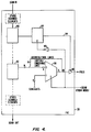
- Fig. 4 illustrates how the PIC is made fully scannable, while at the same time providing fixed outputs during a scan when necessary.
- Fig. 4 shows a one-bit memory element 80, an N-bit memory element 82, an M-bit latch 84, a K-bit 2-to-1 multiplexer 86, an invertor 90, and an N output driver 92.
- the actual configuration may vary from embodiment to embodiment, but the essential features are the same.
- memory element 82 is shown for clarity as a single device, where in some PIC's, the functionality of memory element 82 is distributed throughout the PIC.
- an output enable signal which is output during normal operation of the PIC is output from memory element 80 to latch 84, which outputs its inputs to an enable input of output driver 92, when a signal applied at an enable (E) input of latch 84 is low (active).
- N signals are output from memory element 82 to either multiplexer 86 (K signals) or directly to output driver 92 (M signals).
- the K signals going to multiplexer 86 are control lines coupled to the PBus when a select signal is not asserted (i.e., false, or "0") at a select (S) input to multiplexer 86.
- latch 84 latches its input to its output, and when the S input to multiplexer 86 is asserted (select input set to "1"), multiplexer 86 inputs a preselected set of constants from its "1" input and outputs them onto the K control lines of the PBus.
- any PBus line which is being driven during a scan should be one of the K lines output by multiplexer 86.
- the K signals shown in Table 1 are examples of signals which are always the same value during a scan.
- the first column of Table 1 lists some signals which would be part of the K lines from memory element 82 to the "0" input of multiplexer 86, and the second column shows the constants which would be applied to the "1" input of multiplexer 86.
- At least one memory element maintains a bit indicating whether or not the PIC is the current PBus master. For illustration purposes, assume that this bit is stored in memory element 80. When a scan begins, the scan signal line is set true, causing the E input to latch 84 to go false, which latches the bit onto line 94 which connects to the enable input of output driver 92. By the way, the enable input might fan out to each bit of output driver 92. Also, the K constant bits are output onto the PBus.
Landscapes
- Engineering & Computer Science (AREA)
- General Engineering & Computer Science (AREA)
- Theoretical Computer Science (AREA)
- Computer Hardware Design (AREA)
- Quality & Reliability (AREA)
- Physics & Mathematics (AREA)
- General Physics & Mathematics (AREA)
- Test And Diagnosis Of Digital Computers (AREA)
Applications Claiming Priority (2)
| Application Number | Priority Date | Filing Date | Title |
|---|---|---|---|
| US08/086,341 US5428623A (en) | 1993-07-01 | 1993-07-01 | Scannable interface to nonscannable microprocessor |
| US86341 | 1993-07-01 |
Publications (2)
| Publication Number | Publication Date |
|---|---|
| EP0632383A2 true EP0632383A2 (fr) | 1995-01-04 |
| EP0632383A3 EP0632383A3 (fr) | 1995-09-13 |
Family
ID=22197949
Family Applications (1)
| Application Number | Title | Priority Date | Filing Date |
|---|---|---|---|
| EP94304465A Ceased EP0632383A3 (fr) | 1993-07-01 | 1994-06-20 | Interface balayable pour microprocesseur non-balayable. |
Country Status (7)
| Country | Link |
|---|---|
| US (1) | US5428623A (fr) |
| EP (1) | EP0632383A3 (fr) |
| JP (1) | JPH07146804A (fr) |
| KR (1) | KR100188170B1 (fr) |
| CN (1) | CN1102895A (fr) |
| AU (1) | AU666625B2 (fr) |
| CA (1) | CA2126394C (fr) |
Families Citing this family (10)
| Publication number | Priority date | Publication date | Assignee | Title |
|---|---|---|---|---|
| US5448166A (en) * | 1992-01-03 | 1995-09-05 | Hewlett-Packard Company | Powered testing of mixed conventional/boundary-scan logic |
| FR2693574B1 (fr) * | 1992-07-08 | 1994-09-09 | Sgs Thomson Microelectronics | Procédé pour tester le fonctionnement d'un circuit intégré spécialisé, et circuit intégré spécialisé s'y rapportant. |
| EP0636976B1 (fr) * | 1993-07-28 | 1998-12-30 | Koninklijke Philips Electronics N.V. | MicrocontrÔleur avec support hardware de déverminage par des extensions à boundary scan |
| US5706297A (en) * | 1995-08-24 | 1998-01-06 | Unisys Corporation | System for adapting maintenance operations to JTAG and non-JTAG modules |
| US5793776A (en) * | 1996-10-18 | 1998-08-11 | Samsung Electronics Co., Ltd. | Structure and method for SDRAM dynamic self refresh entry and exit using JTAG |
| FI105727B (fi) * | 1997-05-15 | 2000-09-29 | Nokia Networks Oy | Menetelmä ja järjestely prosessorin liittämiseksi ASIC-piiriin |
| US6092219A (en) * | 1997-12-03 | 2000-07-18 | Micron Technology, Inc. | Method for use of bus parking states to communicate diagnostic information |
| US6112316A (en) * | 1997-12-03 | 2000-08-29 | Micron Electronics, Inc. | System for use of bus parking states to communicate diagnostic information |
| US6363501B1 (en) * | 1998-12-10 | 2002-03-26 | Advanced Micro Devices, Inc. | Method and apparatus for saving and loading peripheral device states of a microcontroller via a scan path |
| US6954879B1 (en) | 1998-12-10 | 2005-10-11 | Advanced Micro Devices, Inc. | Method and apparatus for communicating configuration data for a peripheral device of a microcontroller via a scan path |
Family Cites Families (8)
| Publication number | Priority date | Publication date | Assignee | Title |
|---|---|---|---|---|
| US4023142A (en) * | 1975-04-14 | 1977-05-10 | International Business Machines Corporation | Common diagnostic bus for computer systems to enable testing concurrently with normal system operation |
| NO843375L (no) * | 1983-10-06 | 1985-04-09 | Honeywell Inf Systems | Databehandlingssystem og fremgangsmaate til vedlikehold samt anrodning |
| US4780874A (en) * | 1987-04-20 | 1988-10-25 | Tandem Computers Incorporated | Diagnostic apparatus for a data processing system |
| US5132974A (en) * | 1989-10-24 | 1992-07-21 | Silc Technologies, Inc. | Method and apparatus for designing integrated circuits for testability |
| US5157781A (en) * | 1990-01-02 | 1992-10-20 | Motorola, Inc. | Data processor test architecture |
| US5167781A (en) * | 1990-04-06 | 1992-12-01 | Kemcast Partners-1989 | Continuous plastics molding process and apparatus |
| US5301156A (en) * | 1991-07-18 | 1994-04-05 | Hewlett-Packard Company | Configurable self-test for embedded RAMs |
| US5260649A (en) * | 1992-01-03 | 1993-11-09 | Hewlett-Packard Company | Powered testing of mixed conventional/boundary-scan logic |
-
1993
- 1993-07-01 US US08/086,341 patent/US5428623A/en not_active Expired - Lifetime
-
1994
- 1994-06-20 EP EP94304465A patent/EP0632383A3/fr not_active Ceased
- 1994-06-21 CA CA002126394A patent/CA2126394C/fr not_active Expired - Fee Related
- 1994-06-30 KR KR1019940015396A patent/KR100188170B1/ko not_active Expired - Fee Related
- 1994-06-30 JP JP6149001A patent/JPH07146804A/ja active Pending
- 1994-06-30 AU AU66106/94A patent/AU666625B2/en not_active Ceased
- 1994-07-01 CN CN94108146A patent/CN1102895A/zh active Pending
Also Published As
| Publication number | Publication date |
|---|---|
| AU6610694A (en) | 1995-01-12 |
| US5428623A (en) | 1995-06-27 |
| CA2126394A1 (fr) | 1995-01-02 |
| KR100188170B1 (ko) | 1999-06-01 |
| JPH07146804A (ja) | 1995-06-06 |
| AU666625B2 (en) | 1996-02-15 |
| KR950003973A (ko) | 1995-02-17 |
| CA2126394C (fr) | 1998-10-13 |
| CN1102895A (zh) | 1995-05-24 |
| EP0632383A3 (fr) | 1995-09-13 |
Similar Documents
| Publication | Publication Date | Title |
|---|---|---|
| US6523136B1 (en) | Semiconductor integrated circuit device with processor | |
| EP0511752B1 (fr) | Test à haute vitesse d'un circuit intégré avec JTAG | |
| US6516428B2 (en) | On-chip debug system | |
| US6094730A (en) | Hardware-assisted firmware tracing method and apparatus | |
| US6542844B1 (en) | Method and apparatus for tracing hardware states using dynamically reconfigurable test circuits | |
| US5826093A (en) | Dual function disk drive integrated circuit for master mode and slave mode operations | |
| KR0149891B1 (ko) | 버스상태분석기 및 그 내부버스시험방법 | |
| EP0652516A1 (fr) | Microprocesseur intégré | |
| US5862148A (en) | Microcontroller with improved debug capability for internal memory | |
| WO1999048001A1 (fr) | Ameliorations apportees a des systemes de developpement a microprocesseur | |
| JPH0223891B2 (fr) | ||
| US5428623A (en) | Scannable interface to nonscannable microprocessor | |
| US5900014A (en) | External means of overriding and controlling cacheability attribute of selected CPU accesses to monitor instruction and data streams | |
| JP2006507586A (ja) | 埋め込みシステムの解析装置及び方法 | |
| US6092219A (en) | Method for use of bus parking states to communicate diagnostic information | |
| KR930001584B1 (ko) | 마이크로 컴퓨터 시스템 | |
| US5197143A (en) | Device and method for distributing information in a computer system | |
| KR20060110359A (ko) | 자동차내의 임계 안전 컴퓨터 시스템을 위한 통합형시스템용 디바이스 및 방법 | |
| US5675749A (en) | Method and apparatus for controlling show cycles in a data processing system | |
| US6311303B1 (en) | Monitor port with selectable trace support | |
| US5132973A (en) | Testable embedded RAM arrays for bus transaction buffering | |
| US7231568B2 (en) | System debugging device and system debugging method | |
| US7526691B1 (en) | System and method for using TAP controllers | |
| KR100223096B1 (ko) | 내부 메모리 맵 레지스터를 관측하는 방법 및 장치 | |
| US5826058A (en) | Method and apparatus for providing an external indication of internal cycles in a data processing system |
Legal Events
| Date | Code | Title | Description |
|---|---|---|---|
| PUAI | Public reference made under article 153(3) epc to a published international application that has entered the european phase |
Free format text: ORIGINAL CODE: 0009012 |
|
| AK | Designated contracting states |
Kind code of ref document: A2 Designated state(s): DE FR GB IT SE |
|
| RIN1 | Information on inventor provided before grant (corrected) |
Inventor name: SPROUSE, JEFF A. Inventor name: SABERNICK,FRED C. C/O MRS.N.SABERNICK Inventor name: RAHMAN, MIZANUR MOHAMMED |
|
| PUAL | Search report despatched |
Free format text: ORIGINAL CODE: 0009013 |
|
| AK | Designated contracting states |
Kind code of ref document: A3 Designated state(s): DE FR GB IT SE |
|
| 17P | Request for examination filed |
Effective date: 19960304 |
|
| 17Q | First examination report despatched |
Effective date: 19971013 |
|
| GRAG | Despatch of communication of intention to grant |
Free format text: ORIGINAL CODE: EPIDOS AGRA |
|
| STAA | Information on the status of an ep patent application or granted ep patent |
Free format text: STATUS: THE APPLICATION HAS BEEN REFUSED |
|
| 18R | Application refused |
Effective date: 19990807 |