EP0632489A2 - Méthode de fabrication d'un transistor bipolaire latéral - Google Patents
Méthode de fabrication d'un transistor bipolaire latéral Download PDFInfo
- Publication number
- EP0632489A2 EP0632489A2 EP94109100A EP94109100A EP0632489A2 EP 0632489 A2 EP0632489 A2 EP 0632489A2 EP 94109100 A EP94109100 A EP 94109100A EP 94109100 A EP94109100 A EP 94109100A EP 0632489 A2 EP0632489 A2 EP 0632489A2
- Authority
- EP
- European Patent Office
- Prior art keywords
- zone
- base
- collector
- emitter
- produced
- Prior art date
- Legal status (The legal status is an assumption and is not a legal conclusion. Google has not performed a legal analysis and makes no representation as to the accuracy of the status listed.)
- Withdrawn
Links
Images


Classifications
-
- H—ELECTRICITY
- H10—SEMICONDUCTOR DEVICES; ELECTRIC SOLID-STATE DEVICES NOT OTHERWISE PROVIDED FOR
- H10D—INORGANIC ELECTRIC SEMICONDUCTOR DEVICES
- H10D10/00—Bipolar junction transistors [BJT]
- H10D10/01—Manufacture or treatment
- H10D10/041—Manufacture or treatment of thin-film BJTs
-
- H—ELECTRICITY
- H10—SEMICONDUCTOR DEVICES; ELECTRIC SOLID-STATE DEVICES NOT OTHERWISE PROVIDED FOR
- H10D—INORGANIC ELECTRIC SEMICONDUCTOR DEVICES
- H10D10/00—Bipolar junction transistors [BJT]
- H10D10/311—Thin-film BJTs
-
- Y—GENERAL TAGGING OF NEW TECHNOLOGICAL DEVELOPMENTS; GENERAL TAGGING OF CROSS-SECTIONAL TECHNOLOGIES SPANNING OVER SEVERAL SECTIONS OF THE IPC; TECHNICAL SUBJECTS COVERED BY FORMER USPC CROSS-REFERENCE ART COLLECTIONS [XRACs] AND DIGESTS
- Y10—TECHNICAL SUBJECTS COVERED BY FORMER USPC
- Y10S—TECHNICAL SUBJECTS COVERED BY FORMER USPC CROSS-REFERENCE ART COLLECTIONS [XRACs] AND DIGESTS
- Y10S148/00—Metal treatment
- Y10S148/01—Bipolar transistors-ion implantation
Definitions
- the present invention relates to a method for producing lateral bipolar transistors in silicon.
- a layer sequence for the emitter, base and collector arranged vertically one above the other is customary.
- two zones of the layer sequence are not direct, i. H. accessible from the surface, but must be extended laterally and brought to the surface.
- a further, highly doped buried layer is generally necessary for the bottom doped layer in order to keep the supply line to the surface sufficiently low-resistance.
- the actual transistor, i. H. the npn sequence or the pnp sequence of the layers is not determined photolithographically, but rather by diffusion processes and implantations, so that dimensions in the sub- ⁇ m range can be achieved.
- the object of the present invention is to provide a simple method for the production of lateral bipolar transistors for use in the area of lowest power and reduced supply voltages, this method being intended to enable the integration of npn and pnp transistors in a component without problems.
- lateral bipolar transistors in a thin silicon layer z. B. an SOI substrate.
- the differently doped areas for emitter, base and collector are produced by implanting dopant into a basic doping using masks.
- an auxiliary layer is deposited over the entire area in a trench, a gap between the covered flanks of the trench forming a gap of the width of the base zone to be produced.
- An implantation for the base zone is carried out through this gap, the portions of the auxiliary layer which are present vertically on the trench flanks serving as shielding of the adjacent areas.
- the method according to the invention is advantageously based on an SOI substrate (Silicon on Insulator).
- SOI substrate Silicon on Insulator
- material made with SIMOX or a corresponding layer structure produced by wafer bonding can also be used. It is only important that a thin wear layer made of silicon is applied to an insulating substrate or an insulating intermediate layer and can be processed with the usual methods of silicon technology.
- the method according to the invention is equally suitable for the production of npn transistors as for pnp transistors.
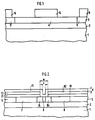
- the z. B. can be 2 microns to 20 nm thick, the area provided for the transistor is laterally isolated all around and provided with a basic doping. It is easiest if the silicon layer is provided with a basic doping of a density of approximately 1015 to 1017 cm ⁇ 3 at the beginning of the process. The sign of this doping is chosen for the conductivity type of emitter and collector. As an example, in the case of an npn transistor, phosphorus or arsenic is introduced as the dopant for the basic doping. The insulation outside of this area provided for the transistor can, for. B. done by LOCOS or by trench etching or the like. A combination of such measures is also possible. The silicon of the silicon layer can also be completely removed outside of this area, so that the transistor is structured in the manner of a mesa. In the exemplary embodiment shown in the figures, the lateral insulation regions 5 are produced by means of LOCOS.
- the substrate 1 shows the substrate 1, the insulation layer 2 and the silicon layer 3.
- the area 4 provided with the basic doping and the lateral insulation areas 5 are shown in cross section in the silicon layer 3.
- the insulation layer 2 can, for. B. SiO2.
- implants of dopants for the connection areas of emitter, collector and base are made.
- the level of doping is selected for a low-resistance metal-semiconductor contact for subsequent electrical contacting.
- the emitter zone 7 and collector zone 8 shown in FIG. 2 are thus obtained.
- the base connection zone highly doped for the opposite sign is perpendicular to the plane of the drawing.
- npn transistor z. B. boron used. Possibly. the implanted areas are then subjected to a healing and / or diffusion process (e.g. RTA / FA processes).
- the order of manufacture of the emitter zone and collector zone and of the base connection zone can be interchanged.
- a polysilicon layer for forming contact layers is then deposited on the silicon above the emitter zone 7 and the collector zone 8 and doped for the conduction type of emitter and collector.
- a dielectric layer is deposited thereon.
- the two deposited layers are structured as shown in FIG. 2, so that there is a contact layer 71 made of polysilicon and a dielectric layer 72 on the emitter zone 7 and a contact layer 81 and a dielectric layer 82 on the collector zone 8.
- the structuring is according to FIG. 2 such that in the middle between emitter zone 7 and collector zone 8, these applied layers leave a trench along the base zone to be produced. The flanks of this trench are vertical.
- auxiliary layer 11 is deposited on this structure over the entire area in conformity with the invention.
- This auxiliary layer 11 has the uniform thickness d.
- the width w of the trench is reduced to a gap of width x.
- the width x of this gap corresponds to the width of the base zone to be produced.
- the dopant for this base zone 9 is then implanted over the entire surface.
- the energy of this implantation is adjusted so that the dopant easily reaches the single-crystalline region of the silicon layer in the region of the gap, but is shielded in the regions to the side of the gap from the portions of the auxiliary layer 11 which are thicker vertically there on the trench flanks. In this way it is achieved that only the area provided for the base zone 9 below the gap is provided with doping.
- the width x of the base zone 9 can be set by the width w of the trench, ie the distance between the contact layers 71, 72, and by the thickness d of the deposited auxiliary layer 11.
- the choice of the thickness of contact layers 71, 81 and dielectric layers 72, 82 can ensure that the dopant for the base zone 9 does not reach the single-crystalline region of the silicon layer outside the region of this base zone.
- the base zone 9 which is produced in this way is then healed.
- Another emitter zone 74 with the basic doping remains between the base zone 9 and the highly doped emitter zone 7.
- Another collector zone 84 with the basic doping remains between the base 9 and the highly doped collector zone 8.
- the auxiliary layer 11 and the dielectric layers 72, 82 are structured with the aid of a photographic technique in such a way that the emitter zone 7, the collector zone 8 and the base connection zone can be provided with metal contacts via contact layers 71, 81 applied thereon.
- a contact layer made of polysilicon can also be applied to the base connection zone, which can be applied together with the contact layers 71, 81 for the emitter and collector, but must be doped in opposite directions.
- Fig. 3 shows in cross section the finished transistor with the applied metal contacts 73, 83 for the emitter and the collector.
- each contact hole can first be filled with the metal contact and then a connection metallization on the surface 70, 80 z. B. applied as part of conductor tracks.
- the gap in the auxiliary layer 11 located above the base zone 9 can e.g. B. can be filled by depositing a dielectric 12. This is possible in each of the embodiments shown.
- FIG. 5 shows the arrangement of the emitter zone 7, the collector zone 8, the base zone 9 and the associated base connection zone 19.
- the contours of the metal contacts 73, 83, 93 attached to these zones are shown in dashed lines.
- a layer of tungsten / TiN or other high-melting metals, metal compounds or polycides (connections of metal with polysilicon) can also be used as the contact layer 71, 81 instead of polysilicon.
- the first metallization level can be carried out entirely with these materials, so that two photolithography steps (contact hole and first metallization level) are omitted.
- the contact layer can also be dispensed with entirely if the emitter zone, the collector zone and the base connection zone are contacted directly with the first metallization level after completion of the diffusion regions. 6, the dielectric layer 72, 82 (z. B. SiO2) is deposited directly on the emitter zone 7, the collector zone 8 and the base connection zone 19.
- This dielectric layer 72, 82 is possibly applied correspondingly thicker than in the previously described exemplary embodiment.
- the trench above the base zone to be produced is first produced in the middle between the emitter zone 7 and the collector zone 8 with the aid of a photographic technique.
- the auxiliary layer 11 is applied over the entire surface, ie with a uniform thickness, so that the gap remains above the base zone 9, through which the doping is introduced into the base zone 9.
- the contact holes are then etched down to the emitter zone 7, the collector zone 8 and the base connection zone 19, so that the metal contacts 73, 83 can be applied directly to these highly doped regions of the original silicon layer, as shown in FIG. 6.
- the width w of the trench above the base zone can be chosen in accordance with the minimum resolution of the photographic technology.
- the distance between the contacts of the emitter and collector is given by this small width w.
- the base zone can be set extremely narrow. Lateral bipolar transistors with extremely small dimensions can therefore be manufactured symmetrically and self-aligned in a simple manner with the method according to the invention.
Landscapes
- Bipolar Transistors (AREA)
Applications Claiming Priority (2)
| Application Number | Priority Date | Filing Date | Title |
|---|---|---|---|
| DE4322135 | 1993-07-02 | ||
| DE4322135 | 1993-07-02 |
Publications (2)
| Publication Number | Publication Date |
|---|---|
| EP0632489A2 true EP0632489A2 (fr) | 1995-01-04 |
| EP0632489A3 EP0632489A3 (fr) | 1996-09-11 |
Family
ID=6491854
Family Applications (1)
| Application Number | Title | Priority Date | Filing Date |
|---|---|---|---|
| EP94109100A Withdrawn EP0632489A3 (fr) | 1993-07-02 | 1994-06-14 | Méthode de fabrication d'un transistor bipolaire latéral. |
Country Status (3)
| Country | Link |
|---|---|
| US (1) | US5407843A (fr) |
| EP (1) | EP0632489A3 (fr) |
| JP (1) | JPH0758122A (fr) |
Family Cites Families (11)
| Publication number | Priority date | Publication date | Assignee | Title |
|---|---|---|---|---|
| US4545113A (en) * | 1980-10-23 | 1985-10-08 | Fairchild Camera & Instrument Corporation | Process for fabricating a lateral transistor having self-aligned base and base contact |
| JPS6081864A (ja) * | 1983-10-12 | 1985-05-09 | Fujitsu Ltd | ラテラル型トランジスタ |
| JP2503460B2 (ja) * | 1986-12-01 | 1996-06-05 | 三菱電機株式会社 | バイポ−ラトランジスタおよびその製造方法 |
| US4922315A (en) * | 1987-11-13 | 1990-05-01 | Kopin Corporation | Control gate lateral silicon-on-insulator bipolar transistor |
| JPH0253630A (ja) * | 1988-08-12 | 1990-02-22 | Daihatsu Motor Co Ltd | 自動車用窓の開閉装置 |
| JPH02244728A (ja) * | 1989-03-17 | 1990-09-28 | Fujitsu Ltd | ラテラル・バイポーラ・トランジスタ |
| US5102812A (en) * | 1989-11-09 | 1992-04-07 | Bell Communications Research | Method of making a lateral bipolar heterojunction structure |
| US5073506A (en) * | 1991-02-14 | 1991-12-17 | Allied-Signal Inc. | Method for making a self-aligned lateral bipolar SOI transistor |
| JP2528559B2 (ja) * | 1991-03-18 | 1996-08-28 | 富士通株式会社 | ラテラルバイポ―ラトランジスタの製造方法 |
| US5164326A (en) * | 1992-03-30 | 1992-11-17 | Motorola, Inc. | Complementary bipolar and CMOS on SOI |
| US5273915A (en) * | 1992-10-05 | 1993-12-28 | Motorola, Inc. | Method for fabricating bipolar junction and MOS transistors on SOI |
-
1994
- 1994-06-14 EP EP94109100A patent/EP0632489A3/fr not_active Withdrawn
- 1994-06-14 US US08/261,142 patent/US5407843A/en not_active Expired - Fee Related
- 1994-06-29 JP JP6170155A patent/JPH0758122A/ja not_active Withdrawn
Also Published As
| Publication number | Publication date |
|---|---|
| US5407843A (en) | 1995-04-18 |
| EP0632489A3 (fr) | 1996-09-11 |
| JPH0758122A (ja) | 1995-03-03 |
Similar Documents
| Publication | Publication Date | Title |
|---|---|---|
| DE3889245T2 (de) | Integrierter und kontrollierter Leistungs-MOSFET. | |
| DE69030415T2 (de) | Verfahren zur Herstellung eines DMOS Transistors | |
| DE69127837T2 (de) | Hochgeschwindigkeits-SOI-Bauelement und Herstellungsverfahren dafür | |
| DE2541548A1 (de) | Isolierschicht-feldeffekttransistor und verfahren zu dessen herstellung | |
| EP0007923A1 (fr) | Procédé pour la fabrication d'un transistor latéral à double diffusion et d'un transistor complémentaire vertical, intégré avec le premier | |
| DE2242026A1 (de) | Mis-feldeffekttransistor | |
| DE4041050A1 (de) | Integrierter schaltkreis | |
| DE3022565A1 (de) | Halbleiteranordnung | |
| EP0687013B1 (fr) | Transistor bipolaire et procédé de fabrication | |
| DE3779802T2 (de) | Verfahren zur herstellung einer halbleiteranordnung. | |
| DE1764570C3 (de) | Verfahren zur Herstellung einer Halbleitervorrichtung mit zueinander komplementären NPN- und PNP-Transistoren | |
| DE2502547A1 (de) | Halbleiterkoerper mit bipolartransistor und verfahren zu dessen herstellung | |
| EP1415340A2 (fr) | Procede de fabrication parallele d'un transistor mos et d'un transistor bipolaire | |
| DE19710731B4 (de) | Leistungshalbleiterbauteil und Verfahren zu dessen Herstellung | |
| DE4143209A1 (de) | Integrierte schaltung | |
| DE3688030T2 (de) | Bipolare integrierte schaltung mit isolationsstruktur und substratkontakt und verfahren zur herstellung. | |
| EP0174022A1 (fr) | Structure d'un transistor | |
| DE112010005265T5 (de) | DMOS-Transistor mit erhöhter Durchbruchsspannung und Verfahren zur Herstellung. | |
| DE68928763T2 (de) | Verfahren zur Herstellung von isolierten vertikalbipolaren und JFET-Transistoren und entsprechender IC | |
| DE10159414A1 (de) | Bipolar-Transistor und Verfahren zum Herstellen desselben | |
| EP0632489A2 (fr) | Méthode de fabrication d'un transistor bipolaire latéral | |
| WO2000019535A1 (fr) | Structure semi-conductrice pour composants a semi-conducteur | |
| DE10345447B4 (de) | Verfahren zum Herstellen eines Halbleiter-Bauteils | |
| EP0740335A2 (fr) | Fabrication de SOI-BiCMOS | |
| EP0632491A2 (fr) | Méthode de fabrication d'un transistor bipolaire latéral |
Legal Events
| Date | Code | Title | Description |
|---|---|---|---|
| PUAI | Public reference made under article 153(3) epc to a published international application that has entered the european phase |
Free format text: ORIGINAL CODE: 0009012 |
|
| AK | Designated contracting states |
Kind code of ref document: A2 Designated state(s): DE FR GB IT NL |
|
| PUAL | Search report despatched |
Free format text: ORIGINAL CODE: 0009013 |
|
| AK | Designated contracting states |
Kind code of ref document: A3 Designated state(s): DE FR GB IT NL |
|
| 17P | Request for examination filed |
Effective date: 19961008 |
|
| 17Q | First examination report despatched |
Effective date: 19991227 |
|
| STAA | Information on the status of an ep patent application or granted ep patent |
Free format text: STATUS: THE APPLICATION IS DEEMED TO BE WITHDRAWN |
|
| 18D | Application deemed to be withdrawn |
Effective date: 20000509 |