EP0632604A1 - Verfahren und Vorrichtung zum Zusammenstellen von basisbandigen Signalen und zur Taktrückgewinnung unter Verwendung eines Konstant-Modulus-Algorithmus - Google Patents
Verfahren und Vorrichtung zum Zusammenstellen von basisbandigen Signalen und zur Taktrückgewinnung unter Verwendung eines Konstant-Modulus-Algorithmus Download PDFInfo
- Publication number
- EP0632604A1 EP0632604A1 EP94110075A EP94110075A EP0632604A1 EP 0632604 A1 EP0632604 A1 EP 0632604A1 EP 94110075 A EP94110075 A EP 94110075A EP 94110075 A EP94110075 A EP 94110075A EP 0632604 A1 EP0632604 A1 EP 0632604A1
- Authority
- EP
- European Patent Office
- Prior art keywords
- signal
- determined
- complex
- phase
- combiner
- Prior art date
- Legal status (The legal status is an assumption and is not a legal conclusion. Google has not performed a legal analysis and makes no representation as to the accuracy of the status listed.)
- Granted
Links
- 238000004422 calculation algorithm Methods 0.000 title claims abstract description 18
- 238000000034 method Methods 0.000 title claims abstract description 14
- 238000011084 recovery Methods 0.000 title abstract description 8
- 238000004891 communication Methods 0.000 claims abstract description 5
- 230000005540 biological transmission Effects 0.000 claims abstract description 3
- 238000005070 sampling Methods 0.000 claims description 18
- 238000005457 optimization Methods 0.000 abstract description 2
- 238000010586 diagram Methods 0.000 description 6
- 230000003993 interaction Effects 0.000 description 4
- 238000004364 calculation method Methods 0.000 description 2
- 230000002238 attenuated effect Effects 0.000 description 1
- 230000006399 behavior Effects 0.000 description 1
- 230000003111 delayed effect Effects 0.000 description 1
- 230000001419 dependent effect Effects 0.000 description 1
- 238000011156 evaluation Methods 0.000 description 1
- 238000012986 modification Methods 0.000 description 1
- 230000004048 modification Effects 0.000 description 1
- 238000012545 processing Methods 0.000 description 1
- 238000004088 simulation Methods 0.000 description 1
Images

Classifications
-
- H—ELECTRICITY
- H04—ELECTRIC COMMUNICATION TECHNIQUE
- H04B—TRANSMISSION
- H04B7/00—Radio transmission systems, i.e. using radiation field
- H04B7/02—Diversity systems; Multi-antenna system, i.e. transmission or reception using multiple antennas
- H04B7/04—Diversity systems; Multi-antenna system, i.e. transmission or reception using multiple antennas using two or more spaced independent antennas
- H04B7/08—Diversity systems; Multi-antenna system, i.e. transmission or reception using multiple antennas using two or more spaced independent antennas at the receiving station
- H04B7/0837—Diversity systems; Multi-antenna system, i.e. transmission or reception using multiple antennas using two or more spaced independent antennas at the receiving station using pre-detection combining
- H04B7/0842—Weighted combining
- H04B7/0848—Joint weighting
- H04B7/0854—Joint weighting using error minimizing algorithms, e.g. minimum mean squared error [MMSE], "cross-correlation" or matrix inversion
Definitions
- the invention relates to a baseband signal combiner and to a sampler to be used typically in radio relay systems but also in generic communication systems.
- One of the drawbacks often occurring in free-space links is the multipath phenomenon. In these circumstances the signal available across the receiving antenna is a combination of various delayed and/or attenuated signals. This combination of signals, in some instances, could lead to the impossibility of maintaining the link.
- a common remedy to this drawback is to resort to space and/or frequency diversity techniques that consist in the use of two suitably spaced antennas in reception or of two transmission frequencies. By combining suitably the two received signals the above-mentioned drawbacks can be compensated for.
- MMSE baseband combiner for microwave digital radio by A.N. D'Avolio, M. Mariano, U. Mengali, A. Spalvieri, published in Conference Record, 2nd European Conference on Radio Relay System pages 235-242, April 1989, there is disclosed a combiner using the MMSE technique and provides a solution to the timing of the sampler by using a special algorithm.
- the first aspect is relative to the interaction between the combiner/sampler and the carrier recovery circuit present in the demodulator.
- a second aspect is relative to the actual cooperation of the combiner and of the sampler with particular regard to the capacity of converging to the optimal condition of operation.
- Fig. 1 the baseband combiner and the diversity signal samplers are shown in the event of only two signals for simplicity.
- Signals 101 and 102 are diversity received, suitably processed and baseband converted signals. Each of the two signals is formed by a phase coincidence component and a quadrature component and therefore it can be represented as a complex signal.
- Signal 101 is fed to the input of a sampling circuit 103 which is composed of two separated devices acting respectively upon the phase coincidence part and upon the quadrature part of the input signal. Both devices are driven by the unique sync signal 105.
- the sampling circuit 103 provides at its output 107 the samples, eventually quantized, of the input signal at the instants established by the sync signal 105.
- Signals 107 and 108 are fed to the input of a combiner 117 which provides at its complex output 116 a suitable linear combination of the inputs, according to the complex coefficients 111 and 112.
- the complex signal 107 is multiplied by the coefficient 111 in the complex multiplier 109; the complex signal 108 is multiplied by the coefficient 112 in the complex multiplier; the complex products 113 and 114 thus obtained are summed in the complex adder 115 providing the combined signal 116.
- a complex multiplier can be realized through four real multipliers and two real summers; similarly a complex adder is formed by two adders that act respectively upon the real and imaginary parts.
- the algorithms for adapting the combiner coefficients 111 and 112 and of the sync signals 105 and 106 are based upon the minimization of a cost function CMA p-q at the output of the combiner, with the method of the stochastic gradient which is a method of iterative minimization based upon a noisy estimate of the cost function gradient.
- This family of cost functions has a double advantage of allowing the acquisition apart from the availability of a data estimate and of being independent of the signal phase thus avoiding any interaction with the circuits devoted to the carrier recovery. Moreover, the application of the same cost function both to the combiner coefficients and to the sync signals assures their cooperation.
- c1 (k) and c2 (k) denote the complex coefficients 111 and 112 of Fig. 1 before updating
- c1 (k+1) and c2 (k+1) denote the values of the same coefficients after updating
- ⁇ c is a positive real constant (step size) that affects the convergence rate and the noiseness of the algorithm in steady condition
- x 1k and x 2k represent the sampled signals 107 and 108
- ( ⁇ )* denotes the complex conjugate relation
- sign [ ⁇ ] denotes the sign operator
- y k is the combined signal 116
- ⁇ 2 is a suitable real constant contained in the definition of CMA function, dependent upon the statistics of the transmitted signal.
- t1 (k) and t2 (k) denote the sampling instants for signals 111 and 112 of Fig. 1 before updating
- t1 (k+1) and t2 (k+1) denote the values of the sampling instants after updating
- ⁇ t is the step size (similar to ⁇ c )
- 1 1k and 2 2k denote the derivatives with respect to time of signal 113 and of signal 114 respectively
- Re ⁇ denote the real part of the complex number and the other symbols have the same meaning as in equations (2) and (3).
- the sampling instants t1 and t2 correspond to the phase of the sync signals 105 and 106.
- Fig. 2 is a block diagram of the circuit controlling the coefficient c1 (signal 111 in Fig. 1).
- Signal 201 is the input signal of the combiner (complex signal 107 in Fig. 1).
- Signal 202 corresponds to combined complex signal 116 in Fig. 1.
- Signal 202 is fed to the input of block 203 which calculates its square module, producing the real output 204 that constitutes the input of the real adder 205.
- the other input 206 of adder 205 is given by the constant ⁇ 2 with its sign reversed: the result 207 of the summation performed by adder 205 is sent to the input of block 208 which calculates its sign 209.
- the multiplier 210 performs the product of the complex signal 202 with the real signal 209. Such product constitutes the complex signal 211.
- Signal 201 is applied to she input of block 212 which calculates its complex conjugate providing it at the output 213.
- Multiplier 214 calculates the product 215 of complex signals 211 and 213.
- Multiplier 216 calculates the product 217 of the complex signal 215 with the real constant ⁇ c (signal 218).
- Block 219 calculates the integral of the input complex signal 217, thus producing the complex output 220 that corresponds to signal 111 of Fig. 1.
- the circuit controlling the coefficient C2 (signal 112 of Fig. 1) is quite similar to the one of Fig. 2; applied to input 201 is now signal 108 of Fig. 1 and, correspondingly, the output 220 coincides with signal 112 of Fig. 1.
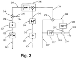
- Fig. 3 is a block diagram of the circuit generating the sync signal 105 of Fig. 1 whose phase determines the sampling instant t1.
- Signal 301 is the signal c1 x 1k (complex signal 113 of Fig. 1).
- Signal 302 corresponds to the complex signal at the output of the combiner (signal 116 of Fig. 1).
- Signal 302 is fed to the input of block 303 which calculates its square modules, providing the real output 304 that constitutes the input of the real adder 305.
- the other input 306 of the adder 305 is given by the constant ⁇ 2 with its sign reversed: the result 307 of the summation performed by adder 305 is fed to the input of block 308 that calculates its sign 309.
- Multiplier 310 performs the product of the complex signal 302 with the real signal 309. Such product constitutes the complex signal 311.
- Signal 301 is fed to block 312 which calculates its derivative with respect to time and provides it at the output 313.
- the complex signal 313 is conjugated in block 314 to generate signal 315.
- Block 316 calculates the real part of the product 317 of the complex signals 311 and 315.
- the multiplier 318 calculates the product 319 of the complex signal 317 with the real constant ⁇ t (signal 320).
- Signal 319 is fed to the input 322 of the voltage controlled oscillator 323; the latter generates the sync signal 324 that corresponds to signal 105 in Fig. 1.
- the circuit for generating the sync signal 106 of Fig. 1 is quite similar to the one of Fig. 3; the input 301 in this circumstance corresponds to the complex signal 114 of Fig. 1, while the output 324 is the sync signal 106 of Fig. 1.
Landscapes
- Physics & Mathematics (AREA)
- Mathematical Physics (AREA)
- Engineering & Computer Science (AREA)
- Computer Networks & Wireless Communication (AREA)
- Signal Processing (AREA)
- Radio Transmission System (AREA)
- Synchronisation In Digital Transmission Systems (AREA)
- Amplitude Modulation (AREA)
- Mobile Radio Communication Systems (AREA)
- Digital Transmission Methods That Use Modulated Carrier Waves (AREA)
- Time-Division Multiplex Systems (AREA)
Applications Claiming Priority (2)
| Application Number | Priority Date | Filing Date | Title |
|---|---|---|---|
| IT93MI001428A IT1264645B1 (it) | 1993-07-02 | 1993-07-02 | Metodo e circuiti di combinazione di segnali in banda base e recupero dei sincronismi di simbolo |
| ITMI931428 | 1993-07-02 |
Publications (2)
| Publication Number | Publication Date |
|---|---|
| EP0632604A1 true EP0632604A1 (de) | 1995-01-04 |
| EP0632604B1 EP0632604B1 (de) | 2001-09-05 |
Family
ID=11366517
Family Applications (1)
| Application Number | Title | Priority Date | Filing Date |
|---|---|---|---|
| EP94110075A Expired - Lifetime EP0632604B1 (de) | 1993-07-02 | 1994-06-29 | Verfahren und Vorrichtung zum Zusammenstellen von basisbandigen Signalen und zur Taktrückgewinnung unter Verwendung eines Konstant-Modulus-Algorithmus |
Country Status (8)
| Country | Link |
|---|---|
| US (1) | US5592516A (de) |
| EP (1) | EP0632604B1 (de) |
| JP (1) | JPH07154442A (de) |
| AT (1) | ATE205342T1 (de) |
| DE (1) | DE69428168T2 (de) |
| ES (1) | ES2162830T3 (de) |
| IT (1) | IT1264645B1 (de) |
| NO (1) | NO309836B1 (de) |
Cited By (3)
| Publication number | Priority date | Publication date | Assignee | Title |
|---|---|---|---|---|
| WO1997026720A1 (en) * | 1996-01-19 | 1997-07-24 | Pcs Wireless (Ip) Inc. | Delay insensitive basestation-to-handset interface for radio telephone systems |
| US6023628A (en) * | 1992-08-05 | 2000-02-08 | Pcs Wireless, Inc. | Base stations for TDD telephony and methods for operating the same |
| EP1315313A1 (de) * | 2001-11-26 | 2003-05-28 | Dataradio Inc. | Vektor-Kombinator für Diversity-Empfang in RF-Transceivers |
Families Citing this family (4)
| Publication number | Priority date | Publication date | Assignee | Title |
|---|---|---|---|---|
| FI105514B (fi) * | 1994-09-12 | 2000-08-31 | Nokia Mobile Phones Ltd | Vastaanottomenetelmä ja vastaanotin |
| US6493838B1 (en) * | 1995-09-29 | 2002-12-10 | Kabushiki Kaisha Toshiba | Coding apparatus and decoding apparatus for transmission/storage of information |
| US6560299B1 (en) * | 1999-07-30 | 2003-05-06 | Christopher H Strolle | Diversity receiver with joint signal processing |
| DE102013003622A1 (de) | 2013-02-18 | 2014-08-21 | Karlsruher Institut für Technologie | Verfahren und Vorrichtung zum Auslesen eines Ein- und/oder Mehrträgersignals |
Family Cites Families (2)
| Publication number | Priority date | Publication date | Assignee | Title |
|---|---|---|---|---|
| US4512034A (en) * | 1983-07-11 | 1985-04-16 | At&T Bell Laboratories | Technique for digital radio space diversity combining |
| US4797950A (en) * | 1986-11-10 | 1989-01-10 | Kenneth Rilling | Multipath reduction system |
-
1993
- 1993-07-02 IT IT93MI001428A patent/IT1264645B1/it active IP Right Grant
-
1994
- 1994-06-24 NO NO942408A patent/NO309836B1/no not_active IP Right Cessation
- 1994-06-29 AT AT94110075T patent/ATE205342T1/de not_active IP Right Cessation
- 1994-06-29 ES ES94110075T patent/ES2162830T3/es not_active Expired - Lifetime
- 1994-06-29 EP EP94110075A patent/EP0632604B1/de not_active Expired - Lifetime
- 1994-06-29 DE DE69428168T patent/DE69428168T2/de not_active Expired - Lifetime
- 1994-07-01 US US08/270,140 patent/US5592516A/en not_active Expired - Lifetime
- 1994-07-04 JP JP6173098A patent/JPH07154442A/ja active Pending
Non-Patent Citations (3)
| Title |
|---|
| A.N.D'ANDREA ET AL.: ""MMSE BASEBAND COMBINER FOR DIGITAL MICROWAVE RADIO", TELETTRA REVIEW, no. 44, 1989, ITALY, pages 43 - 48 * |
| PROCEEDINGS OF 1986 IEEE MILITARY COMMUNICATIONS CONFERENCE - MILCOM '86 5-9 October 1986, Monterey, California (US) NEW YORK (US) * |
| T.OHGANE: "CHARACTERISTICS OF CMA ADAPTIVE ARRAY FOR SELECTIVE FADING COMPENSATION IN DIGITAL LAND MOBILE RADIO COMMUNICATIONS", ELECTRONICS & COMMUNICATIONS IN JAPAN, PART I - COMMUNICATIONS, vol. 74, no. 9, September 1991 (1991-09-01), NEW YORK US, pages 43 - 53, XP000291519 * |
Cited By (4)
| Publication number | Priority date | Publication date | Assignee | Title |
|---|---|---|---|---|
| US6023628A (en) * | 1992-08-05 | 2000-02-08 | Pcs Wireless, Inc. | Base stations for TDD telephony and methods for operating the same |
| WO1997026720A1 (en) * | 1996-01-19 | 1997-07-24 | Pcs Wireless (Ip) Inc. | Delay insensitive basestation-to-handset interface for radio telephone systems |
| EP1315313A1 (de) * | 2001-11-26 | 2003-05-28 | Dataradio Inc. | Vektor-Kombinator für Diversity-Empfang in RF-Transceivers |
| US7103118B2 (en) | 2001-11-26 | 2006-09-05 | Dataradio Inc. | Vectorial combiner for diversity reception in RF tranceivers |
Also Published As
| Publication number | Publication date |
|---|---|
| ES2162830T3 (es) | 2002-01-16 |
| NO309836B1 (no) | 2001-04-02 |
| IT1264645B1 (it) | 1996-10-04 |
| DE69428168T2 (de) | 2002-05-16 |
| US5592516A (en) | 1997-01-07 |
| NO942408D0 (de) | 1994-06-24 |
| DE69428168D1 (de) | 2001-10-11 |
| JPH07154442A (ja) | 1995-06-16 |
| NO942408L (no) | 1995-01-03 |
| ITMI931428A1 (it) | 1995-01-02 |
| EP0632604B1 (de) | 2001-09-05 |
| ATE205342T1 (de) | 2001-09-15 |
| ITMI931428A0 (it) | 1993-07-02 |
Similar Documents
| Publication | Publication Date | Title |
|---|---|---|
| US5875215A (en) | Carrier synchronizing unit | |
| KR950006765B1 (ko) | 복합 적응형 등화기의 계수 갱신방법 및 그 장치 | |
| US6987815B2 (en) | Receive method and receiver in communication system | |
| CA2036423C (en) | Method of reducing the influence of fading of a viterbi receiver having at least two antennas | |
| US5377226A (en) | Fractionally-spaced equalizer for a DS-CDMA system | |
| US8583068B2 (en) | Interference reduction for multiple signals | |
| US4328585A (en) | Fast adapting fading channel equalizer | |
| US4281411A (en) | High speed digital communication receiver | |
| US5425060A (en) | Mechanism for reducing timing jitter in clock recovery scheme for blind acquisition of full duplex signals | |
| US5920286A (en) | Stabilisation of phased array antennas | |
| EP0397386B1 (de) | Diversity-Empfängeranordnung für digitale Signale | |
| EP0613260A2 (de) | Raumdiversityempfänger für ein digitales Kommunikationssystem | |
| GB2199468A (en) | Techniques for cross-polarization cancellation in a space diversity radio system | |
| KR20010068616A (ko) | 디지털 티브이의 채널 등화기 | |
| US5379046A (en) | Interference wave canceller | |
| EP0853388A2 (de) | Phasenkorrekturverfahren und -gerät für einen drahtlosen Spreizspektrumempfänger | |
| EP0632604A1 (de) | Verfahren und Vorrichtung zum Zusammenstellen von basisbandigen Signalen und zur Taktrückgewinnung unter Verwendung eines Konstant-Modulus-Algorithmus | |
| US5519735A (en) | Reconstructing a primary signal from many secondary signals | |
| JP2785858B2 (ja) | 高速制御適応フィルタを用いた受信方式 | |
| JP3851478B2 (ja) | 適応アレーアンテナ装置 | |
| DE19606102A1 (de) | Verfahren zum Ausgleich des Gleichspannungsstöranteils von Empfangssignalen und derartig ausgestaltete Empfangseinrichtung bzw. Funkstation | |
| US6564044B1 (en) | Simultaneous processing of multiple signals by an adaptive antenna | |
| CA1128160A (en) | Sampling clock correction circuit | |
| NO174609B (no) | Adaptiv frekvensdomeneutjevner for digitale radiolinjesystemer (D LS) | |
| KR950012821B1 (ko) | 디지탈 비순환형 필터 형태의 등화기를 갖는 vhf카 라디오 |
Legal Events
| Date | Code | Title | Description |
|---|---|---|---|
| PUAI | Public reference made under article 153(3) epc to a published international application that has entered the european phase |
Free format text: ORIGINAL CODE: 0009012 |
|
| AK | Designated contracting states |
Kind code of ref document: A1 Designated state(s): AT BE CH DE ES FR GB LI NL SE |
|
| 17P | Request for examination filed |
Effective date: 19950620 |
|
| 17Q | First examination report despatched |
Effective date: 19990729 |
|
| RAP1 | Party data changed (applicant data changed or rights of an application transferred) |
Owner name: ALCATEL |
|
| GRAG | Despatch of communication of intention to grant |
Free format text: ORIGINAL CODE: EPIDOS AGRA |
|
| GRAG | Despatch of communication of intention to grant |
Free format text: ORIGINAL CODE: EPIDOS AGRA |
|
| GRAH | Despatch of communication of intention to grant a patent |
Free format text: ORIGINAL CODE: EPIDOS IGRA |
|
| GRAH | Despatch of communication of intention to grant a patent |
Free format text: ORIGINAL CODE: EPIDOS IGRA |
|
| GRAA | (expected) grant |
Free format text: ORIGINAL CODE: 0009210 |
|
| AK | Designated contracting states |
Kind code of ref document: B1 Designated state(s): AT BE CH DE ES FR GB LI NL SE |
|
| PG25 | Lapsed in a contracting state [announced via postgrant information from national office to epo] |
Ref country code: NL Free format text: LAPSE BECAUSE OF FAILURE TO SUBMIT A TRANSLATION OF THE DESCRIPTION OR TO PAY THE FEE WITHIN THE PRESCRIBED TIME-LIMIT Effective date: 20010905 Ref country code: LI Free format text: LAPSE BECAUSE OF FAILURE TO SUBMIT A TRANSLATION OF THE DESCRIPTION OR TO PAY THE FEE WITHIN THE PRESCRIBED TIME-LIMIT Effective date: 20010905 Ref country code: CH Free format text: LAPSE BECAUSE OF FAILURE TO SUBMIT A TRANSLATION OF THE DESCRIPTION OR TO PAY THE FEE WITHIN THE PRESCRIBED TIME-LIMIT Effective date: 20010905 Ref country code: BE Free format text: LAPSE BECAUSE OF FAILURE TO SUBMIT A TRANSLATION OF THE DESCRIPTION OR TO PAY THE FEE WITHIN THE PRESCRIBED TIME-LIMIT Effective date: 20010905 |
|
| REF | Corresponds to: |
Ref document number: 205342 Country of ref document: AT Date of ref document: 20010915 Kind code of ref document: T |
|
| REG | Reference to a national code |
Ref country code: CH Ref legal event code: EP |
|
| PG25 | Lapsed in a contracting state [announced via postgrant information from national office to epo] |
Ref country code: AT Free format text: LAPSE BECAUSE OF FAILURE TO SUBMIT A TRANSLATION OF THE DESCRIPTION OR TO PAY THE FEE WITHIN THE PRESCRIBED TIME-LIMIT Effective date: 20010919 |
|
| REF | Corresponds to: |
Ref document number: 69428168 Country of ref document: DE Date of ref document: 20011011 |
|
| ET | Fr: translation filed | ||
| PG25 | Lapsed in a contracting state [announced via postgrant information from national office to epo] |
Ref country code: SE Free format text: LAPSE BECAUSE OF FAILURE TO SUBMIT A TRANSLATION OF THE DESCRIPTION OR TO PAY THE FEE WITHIN THE PRESCRIBED TIME-LIMIT Effective date: 20011205 |
|
| REG | Reference to a national code |
Ref country code: GB Ref legal event code: IF02 |
|
| REG | Reference to a national code |
Ref country code: ES Ref legal event code: FG2A Ref document number: 2162830 Country of ref document: ES Kind code of ref document: T3 |
|
| NLV1 | Nl: lapsed or annulled due to failure to fulfill the requirements of art. 29p and 29m of the patents act | ||
| REG | Reference to a national code |
Ref country code: CH Ref legal event code: PL |
|
| PLBE | No opposition filed within time limit |
Free format text: ORIGINAL CODE: 0009261 |
|
| STAA | Information on the status of an ep patent application or granted ep patent |
Free format text: STATUS: NO OPPOSITION FILED WITHIN TIME LIMIT |
|
| 26N | No opposition filed | ||
| PGFP | Annual fee paid to national office [announced via postgrant information from national office to epo] |
Ref country code: ES Payment date: 20030616 Year of fee payment: 10 |
|
| PG25 | Lapsed in a contracting state [announced via postgrant information from national office to epo] |
Ref country code: ES Free format text: LAPSE BECAUSE OF NON-PAYMENT OF DUE FEES Effective date: 20040630 |
|
| REG | Reference to a national code |
Ref country code: ES Ref legal event code: FD2A Effective date: 20040630 |
|
| REG | Reference to a national code |
Ref country code: FR Ref legal event code: CD |
|
| PGFP | Annual fee paid to national office [announced via postgrant information from national office to epo] |
Ref country code: FR Payment date: 20110630 Year of fee payment: 18 |
|
| PGFP | Annual fee paid to national office [announced via postgrant information from national office to epo] |
Ref country code: GB Payment date: 20110620 Year of fee payment: 18 |
|
| PGFP | Annual fee paid to national office [announced via postgrant information from national office to epo] |
Ref country code: DE Payment date: 20110622 Year of fee payment: 18 |
|
| GBPC | Gb: european patent ceased through non-payment of renewal fee |
Effective date: 20120629 |
|
| REG | Reference to a national code |
Ref country code: FR Ref legal event code: ST Effective date: 20130228 |
|
| REG | Reference to a national code |
Ref country code: DE Ref legal event code: R119 Ref document number: 69428168 Country of ref document: DE Effective date: 20130101 |
|
| PG25 | Lapsed in a contracting state [announced via postgrant information from national office to epo] |
Ref country code: GB Free format text: LAPSE BECAUSE OF NON-PAYMENT OF DUE FEES Effective date: 20120629 Ref country code: DE Free format text: LAPSE BECAUSE OF NON-PAYMENT OF DUE FEES Effective date: 20130101 Ref country code: FR Free format text: LAPSE BECAUSE OF NON-PAYMENT OF DUE FEES Effective date: 20120702 |