EP0632646A2 - Anzeigevorrichtung mit aktiver Matrix - Google Patents
Anzeigevorrichtung mit aktiver Matrix Download PDFInfo
- Publication number
- EP0632646A2 EP0632646A2 EP94110124A EP94110124A EP0632646A2 EP 0632646 A2 EP0632646 A2 EP 0632646A2 EP 94110124 A EP94110124 A EP 94110124A EP 94110124 A EP94110124 A EP 94110124A EP 0632646 A2 EP0632646 A2 EP 0632646A2
- Authority
- EP
- European Patent Office
- Prior art keywords
- stage section
- columns
- display
- picture elements
- shift register
- Prior art date
- Legal status (The legal status is an assumption and is not a legal conclusion. Google has not performed a legal analysis and makes no representation as to the accuracy of the status listed.)
- Granted
Links
Images



Classifications
-
- H—ELECTRICITY
- H04—ELECTRIC COMMUNICATION TECHNIQUE
- H04N—PICTORIAL COMMUNICATION, e.g. TELEVISION
- H04N3/00—Scanning details of television systems; Combination thereof with generation of supply voltages
- H04N3/10—Scanning details of television systems; Combination thereof with generation of supply voltages by means not exclusively optical-mechanical
- H04N3/12—Scanning details of television systems; Combination thereof with generation of supply voltages by means not exclusively optical-mechanical by switched stationary formation of lamps, photocells or light relays
-
- H—ELECTRICITY
- H04—ELECTRIC COMMUNICATION TECHNIQUE
- H04N—PICTORIAL COMMUNICATION, e.g. TELEVISION
- H04N3/00—Scanning details of television systems; Combination thereof with generation of supply voltages
- H04N3/10—Scanning details of television systems; Combination thereof with generation of supply voltages by means not exclusively optical-mechanical
- H04N3/12—Scanning details of television systems; Combination thereof with generation of supply voltages by means not exclusively optical-mechanical by switched stationary formation of lamps, photocells or light relays
- H04N3/127—Scanning details of television systems; Combination thereof with generation of supply voltages by means not exclusively optical-mechanical by switched stationary formation of lamps, photocells or light relays using liquid crystals
-
- G—PHYSICS
- G09—EDUCATION; CRYPTOGRAPHY; DISPLAY; ADVERTISING; SEALS
- G09G—ARRANGEMENTS OR CIRCUITS FOR CONTROL OF INDICATING DEVICES USING STATIC MEANS TO PRESENT VARIABLE INFORMATION
- G09G3/00—Control arrangements or circuits, of interest only in connection with visual indicators other than cathode-ray tubes
- G09G3/20—Control arrangements or circuits, of interest only in connection with visual indicators other than cathode-ray tubes for presentation of an assembly of a number of characters, e.g. a page, by composing the assembly by combination of individual elements arranged in a matrix no fixed position being assigned to or needed to be assigned to the individual characters or partial characters
- G09G3/34—Control arrangements or circuits, of interest only in connection with visual indicators other than cathode-ray tubes for presentation of an assembly of a number of characters, e.g. a page, by composing the assembly by combination of individual elements arranged in a matrix no fixed position being assigned to or needed to be assigned to the individual characters or partial characters by control of light from an independent source
- G09G3/36—Control arrangements or circuits, of interest only in connection with visual indicators other than cathode-ray tubes for presentation of an assembly of a number of characters, e.g. a page, by composing the assembly by combination of individual elements arranged in a matrix no fixed position being assigned to or needed to be assigned to the individual characters or partial characters by control of light from an independent source using liquid crystals
- G09G3/3611—Control of matrices with row and column drivers
- G09G3/3685—Details of drivers for data electrodes
- G09G3/3688—Details of drivers for data electrodes suitable for active matrices only
-
- G—PHYSICS
- G09—EDUCATION; CRYPTOGRAPHY; DISPLAY; ADVERTISING; SEALS
- G09G—ARRANGEMENTS OR CIRCUITS FOR CONTROL OF INDICATING DEVICES USING STATIC MEANS TO PRESENT VARIABLE INFORMATION
- G09G2310/00—Command of the display device
- G09G2310/02—Addressing, scanning or driving the display screen or processing steps related thereto
- G09G2310/0232—Special driving of display border areas
-
- G—PHYSICS
- G09—EDUCATION; CRYPTOGRAPHY; DISPLAY; ADVERTISING; SEALS
- G09G—ARRANGEMENTS OR CIRCUITS FOR CONTROL OF INDICATING DEVICES USING STATIC MEANS TO PRESENT VARIABLE INFORMATION
- G09G2340/00—Aspects of display data processing
- G09G2340/04—Changes in size, position or resolution of an image
- G09G2340/0442—Handling or displaying different aspect ratios, or changing the aspect ratio
-
- G—PHYSICS
- G09—EDUCATION; CRYPTOGRAPHY; DISPLAY; ADVERTISING; SEALS
- G09G—ARRANGEMENTS OR CIRCUITS FOR CONTROL OF INDICATING DEVICES USING STATIC MEANS TO PRESENT VARIABLE INFORMATION
- G09G2340/00—Aspects of display data processing
- G09G2340/04—Changes in size, position or resolution of an image
- G09G2340/0464—Positioning
- G09G2340/0478—Horizontal positioning
-
- G—PHYSICS
- G09—EDUCATION; CRYPTOGRAPHY; DISPLAY; ADVERTISING; SEALS
- G09G—ARRANGEMENTS OR CIRCUITS FOR CONTROL OF INDICATING DEVICES USING STATIC MEANS TO PRESENT VARIABLE INFORMATION
- G09G2360/00—Aspects of the architecture of display systems
- G09G2360/02—Graphics controller able to handle multiple formats, e.g. input or output formats
-
- G—PHYSICS
- G09—EDUCATION; CRYPTOGRAPHY; DISPLAY; ADVERTISING; SEALS
- G09G—ARRANGEMENTS OR CIRCUITS FOR CONTROL OF INDICATING DEVICES USING STATIC MEANS TO PRESENT VARIABLE INFORMATION
- G09G3/00—Control arrangements or circuits, of interest only in connection with visual indicators other than cathode-ray tubes
- G09G3/20—Control arrangements or circuits, of interest only in connection with visual indicators other than cathode-ray tubes for presentation of an assembly of a number of characters, e.g. a page, by composing the assembly by combination of individual elements arranged in a matrix no fixed position being assigned to or needed to be assigned to the individual characters or partial characters
- G09G3/2007—Display of intermediate tones
- G09G3/2011—Display of intermediate tones by amplitude modulation
-
- H—ELECTRICITY
- H04—ELECTRIC COMMUNICATION TECHNIQUE
- H04N—PICTORIAL COMMUNICATION, e.g. TELEVISION
- H04N5/00—Details of television systems
- H04N5/66—Transforming electric information into light information
- H04N5/70—Circuit details for electroluminescent devices
-
- H—ELECTRICITY
- H04—ELECTRIC COMMUNICATION TECHNIQUE
- H04N—PICTORIAL COMMUNICATION, e.g. TELEVISION
- H04N7/00—Television systems
- H04N7/01—Conversion of standards, e.g. involving analogue television standards or digital television standards processed at pixel level
- H04N7/0117—Conversion of standards, e.g. involving analogue television standards or digital television standards processed at pixel level involving conversion of the spatial resolution of the incoming video signal
- H04N7/0122—Conversion of standards, e.g. involving analogue television standards or digital television standards processed at pixel level involving conversion of the spatial resolution of the incoming video signal the input and the output signals having different aspect ratios
Definitions
- This invention relates generally to an active matrix display device, and particularly to a driving system for an active matrix display device which can change over between a display of the aspect ratio of 16:9 and another display of the aspect ratio of 4:3 and also to a horizontal shift register for driving an active matrix display device by line sequential horizontal driving.
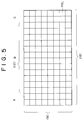
- An active matrix display device conforming to the high definition television standards has such a horizontally elongated screen as shown in FIG. 5 and allows a display of the aspect ratio of 16:9 (such display will be hereinafter referred to as wide display).
- a large number of picture elements PXL are disposed in rows and columns on the screen so as to satisfy the aspect ratio of 16:9.
- another active matrix display device having an ordinary screen size performs another display of the aspect ratio of 4:3 (such display will be hereinafter referred to as normal display).
- a structure which allows changing over between a wide display and a normal display is known.
- FIGS. 6(A) and 6(B) Various means have been proposed for a changing over method between a wide display and a normal display.
- One of such methods involves compression processing of a video signal as illustrated in FIGS. 6(A) and 6(B).
- a video signal for a normal display is inputted as seen from the waveform of FIG. 6(A), it is first converted by A/D conversion into digital data.
- compression processing for each one horizontal period (1H) is performed at a desired ratio as seen from the waveform of FIG. 6(2).
- the digital data obtained by the compression processing is distributed to the area B while fixed data for a masked display are supplied to the areas A and C (FIG. 5) on the opposite sides of the area B.
- an active matrix display device which comprises a plurality of picture elements disposed in rows and columns on a horizontally elongated screen, the columns of the picture elements being divided into a first area allocated to a normal display and a second area included in a wide display, a gate line connected to each of the rows of the picture elements, a vertical drive circuit connected to the gate lines, a data line connected to each of the columns of the picture elements, a signal line for supplying a video signal, a plurality of sampling switches for interconnecting the signal line and the data lines, and a horizontal shift register for controlling sequential opening and closing operations of the sampling switches, the horizontal shift register being divided into a predetermined stage section which corresponds to those of the columns of the picture elements in the first area and an expansion stage section which corresponds to those of the columns of the picture elements in the second area.
- the shift register is divided into a first stage section, a second stage section, and a third stage section, and the predetermined station section corresponds to the second stage section while the expansion stage section corresponds to the first and third stage sections.
- the active matrix display device further comprises a first gate circuit connected to an input terminal of the first stage section, a second gate circuit interposed between an output of the first stage section and an input terminal of the second stage section, a third gate circuit interposed between an output terminal of the second stage section and an input terminal of the third stage section, and means for switchably controlling the first, second and third gate circuits.
- the active matrix display device further comprises masking means for supplying, upon normal display, a signal of a fixed level to those of the data lines which belong to the second area to mask the second area.
- the horizontal shift register which is constituted from a multiple connection of flipflops, is divided into the predetermined stage section and the expansion stage section.
- the predetermined stage section corresponds to a normal display while the expansion stage section corresponds to an expansion area when wide display is performed.
- the predetermined stage section and the expansion stage section are interconnected by way of the gate circuits.
- the predetermined stage section and the expansion stage section are serially connected to each other into an integrated condition by way of the gate circuits, but in a normal display, the expansion stage section is disconnected from the predetermined stage section.
- the active matrix display device is advantageous in terms of the cost since particularly complicated digital processing of a video signal is not required.
- a horizontal shift register which comprises a first stage section corresponding to columns of normal display picture elements allocated to a normal when the normal display is provided by part of a horizontally elongated screen, a second stage section corresponding to columns of wide display picture elements included in a wide display when the wide display is provided by the entire horizontally elongated screen, and means for controlling connection and disconnection between the first and second stage sections such that, upon wide display, the first and second stage sections are serially connected into an integrated condition so as to effect sequential selection control of all of the columns of the normal display picture elements and the wide display picture elements, but upon normal display, the second stage section is disconnected from the first stage section so as to effect sequential selection control of the columns only of the normal display picture elements.
- the horizontal shift register further comprise masking means for masking the columns of the wide display picture elements upon normal display.
- FIG. 1 there is shown a basic construction of an active matrix display device according to the present invention.
- the active matrix display device shown includes a plurality of picture elements (PXL) disposed in rows and columns on a horizontally elongated screen.
- a gate line 1 is connected to each of the rows of the picture element.
- a vertical driver or vertical drive circuit 2 is connected to the gate lines 1.
- a data line 3 is connected to each of the columns of the picture elements.
- a signal line 4 is disposed for supplying a video signal or image signal Vsig to the picture elements.
- the signal line 4 and the data lines 3 are connected to each other by way of a plurality of sampling switches SW.
- the sampling switches SW are sequentially operated to open or close under the control of a horizontal shift register (SR) by way of a horizontal driver 5.
- SR horizontal shift register
- the picture element columns of the horizontally elongated screen are divided into a predetermined area allocated to a normal display and a pair of expansion areas included in a wide display.
- the predetermined area includes the picture element columns from the L+lth to Mth picture element columns both inclusive while the expansion areas include the picture element columns from the first to Lth picture element columns both inclusive and from the M+lth to Nth picture element columns both inclusive.
- the horizontal shift register (SR) is divided into three stage sections including a predetermined stage section SRB corresponding to the picture element columns of the predetermined area and a pair of expansion stage sections SRA and SRC corresponding to the picture element columns of the expansion areas.
- the predetermined stage section SRB and the expansion stage sections SRA and SRC of the horizontal shift register are serially connected into an integrated condition and sequentially operate the sampling switches SW to open or close.
- the expansion stage sections SRA and SRB of the horizontal shift register (SR) are disconnected from the predetermined stage section SRB and only those of the sampling switches SW which belong to the predetermined area are sequentially operated to open or close.
- the horizontal shift register is divided into three portions including the expansion front stage section SRA, the predetermined middle stage section SRB, and the expansion rear stage section SRC.
- a first gate circuit G0 is connected to an input terminal of the expansion front stage section SRA.
- a second gate circuit G1 is interposed between an output terminal of the expansion front stage section SRA and an input terminal of the predetermined middle stage section SRB.
- a third gate circuit G2 is interposed between an output terminal of the predetermined middle stage section SRB and an input terminal of the expansion rear stage section SRC.
- the gate circuits G0, G1 and G2 are controlled to be switched by control signals CTL0, CTL1 and CTL2, respectively, to selectively perform connection integration and disconnection of the horizontal shift register.
- a start signal ST for the shift register is supplied to the first gate circuit G0 at the top of the three gate circuits G0, G1 and G2.
- the active matrix display device further includes masking means, and upon normal display, a signal (masking signal) of a fixed level is supplied to those of the data lines 3 which belong to the expansion areas to selectively effect masked display of the expansion areas (side black display).
- the masking means is constituted from a plurality of gate elements GA which belong to one of the expansion areas, another plurality of gate elements GB which belong to the central predetermined area, and a further plurality of gate elements GC which belong to the other expansion area.
- the gate elements GA are individually connected to those of the gate lines 3 which correspond to the first to Lth picture element columns.
- the gate elements GB are individually connected to those of the gate lines 3 which correspond to the L+lth to Mth picture element columns.
- the gate elements GC are connected to those of the gate lines 3 which corresponds to the M+lth to Nth picture element columns.
- the gate elements GA and GC receive a masking signal MSKA, and the gate electrodes GB receives another masking signal MSKB.
- the gate elements GA and GC are controlled to be opened or closed by a control signal CTLA, and the gate aliments GB are controlled to be opened or closed by another control signal CTLB.
- FIG. 2 shows a detailed circuit construction of the gate circuits G0, G1 and G2.
- the first gate circuit G0 is constituted from a pair of AND elements AND1 and AND2.
- the second gate circuit G1 is constituted from a pair of AND elements AND3 and AND4 and a single OR circuit OR1.
- the third gate circuit G2 is constituted from a single AND element AND5. In the construction, when wide display is effected, all of the control signals CTL0, CTL1 and CTL2 are set to a low level by an external control circuit.
- control signals CTL0, CTL1 and CTL2 may be supplied from a common control line.
- the control signal CTL0 is set to a low level
- the AND element AND1 is closed while the AND element AND2 is opened.
- a start signal ST inputted to the first gate circuit G0 is supplied to the expansion front stage section SRA of the horizontal shift register by way of the AND element AND2.
- the expansion front stage section SRA sequentially transfers the start signal ST in synchronism with a predetermined clock signal to sequentially open the sampling switches SW corresponding to the first column to the Lth column by way of the horizontal driver 5 (FIG. 1).
- a video signal Vsig supplied from the signal line 4 is sampled to those of the data lines 3 which correspond to the picture element columns from the first column to the Lth column.
- the AND element AND3 is in a closed condition while the AND element AND4 is in an open condition. Consequently, an output signal of the expansion front stage section SRA is supplied to an input terminal of the predetermined middle stage section SRB by way of the AND element AND4 and the OR circuit OR1.
- the predetermined middle stage section SRB sequentially performs signal transfer in a similar manner as described above to control and drive the corresponding L+lth to Mth picture element columns.
- the AND element AND5 of the third gate circuit G2 is in an open state. Accordingly, an output signal of the predetermined middle stage section SRB passes the AND element AND5 and is inputted to the expansion rear stage section SRC.
- the expansion rear stage section SRC performs signal transfer in a similar manner as described above to control and sequentially drive the corresponding M+lth to Nth picture element columns. As a result of the operation described above, all of the first to Nth picture element columns are sequentially driven to effect wide display.
- the control signals CTL0, CTL1 and CTL2 are set to a high level.
- the AND element AND1 of the first gate circuit G0 is opened, and AND element AND2 is closed.
- a start signal ST inputted to the first gate circuit G0 is inputted to the second gate circuit G1 through the AND element AND1. Consequently, the expansion front stage section SRA of the horizontal shift register is put into a disconnected condition.
- the control signal CTL1 is at a high level
- the AND element AND3 of the second gate circuit G1 is opened and the AND element AND4 is closed. Consequently, the start signal ST passes the AND element AND3 and the OR circuit OR1 and is supplied to the input terminal of the predetermined middle stage section SRB.
- the predetermined middle stage section SRB sequentially transfers the start signal ST to drive the corresponding L+lth to Mth picture element columns by way of the horizontal driver 5 and the corresponding switching elements SW. Finally, when the control signal CTL2 is at a high level, the AND element AND5 of the third gate circuit G2 is in a closed condition. Consequently, an output signal of the predetermined middle stage section SRB cannot pass the third gate circuit G2. Consequently, the expansion rear stage section SRC is put into a disconnected condition. Due to the operations described above, upon normal display, only the predetermined middle stage section SRB effects a signal transfer operation.
- FIG. 3 is a circuit diagram showing a detailed construction example of the masking means described above.
- a picture element array 10 constituting the horizontally elongated screen is divided into a predetermined area 11B allocated to a normal display and a pair of expansion areas 12A and 12B included in a wide display.
- the first to Lth picture element columns belong to the expansion area 12A; the L+lth to Mth picture element columns belong to the central predetermined area 11B; and the M+lth to Nth picture element columns are included in the other expansion area 11C.
- the gate elements GA disposed for the expansion area 12A are individually constituted from transmission gates and connected to the corresponding data lines 3.
- the gate elements GB disposed in the predetermined area 11B are formed from transmission gates and individually connected to the corresponding data lines 3.
- the gate elements GC disposed in the expansion area 12C are formed from transmission gates and individually connected to the corresponding data lines 3.
- a predetermined masking signal MSKA is supplied to the gate elements GA and GC which belong to the expansion areas 12A and 12C while another masking signal MSKB is supplied to the gate elements GB which belong to the predetermined area 11B.
- a control signal CTLA and another control signal CTLA ⁇ which is an inverted signal of the control signal CTLA and accordingly is indicated by CTLA with an upper horizontal bar applied thereto, are applied to control terminals of the transmission gate elements GA and GC.
- Another pair of control signals CTLBL and CTLBH are supplied to control terminals of the transmission gate elements GB.
- the control signal CTLA upon normal display, the control signal CTLA is set to a high level so that the gate elements GA and GC are put into an open state. Consequently, the masking signal MSKA having a predetermined level is distributed to the expansion areas 12A and 12C by way of the gate elements GA and GC, respectively, so that a desired masked display is provided.
- the control signal CTLA upon wide display, the control signal CTLA is changed over to a low level so that the gate elements 12A and 12C are put into a closed state. Consequently, the masking signal MSKA is not supplied to the expansion areas 12A and 12C. Meanwhile, since a video signal is supplied to the entire picture element array 10 by way of the sampling switches SW (FIG. 1) as described hereinabove, desired masked display is performed.
- the control signal CTLBL is always set to a low level while the control signal CTLBH is always set to a high level. Consequently, in any of a wide display and a normal display, the gate elements GB which belong to the predetermined area 11B remain in a disconnected condition. Consequently, the masking signal MSKB is not supplied to the predetermined area 11B at all. In this manner, since the gate elements GB remain in a normally off state, they need not necessarily be incorporated in the circuit. However, actually it is preferable to add the gate elements GB having an equal size as dummy gates to those of the gate elements GA and GC in order to make the loads to all of the data lines 3 equal among them. Since the gate elements GB are normally off, the masking signal MSKB may be set to any level in principle. Actually, it is preferable to set it to a level at which the leak current of the gate elements GB exhibits a minimum level.
- the active matrix display device includes various displays such as, for example, a liquid crystal displays, a plasma display, and a plasma addressed liquid crystal display.
- each picture element is constituted from a picture element electrode, a thin film transistor and so forth.
- the gate electrode of the thin film transistor is connected to a corresponding gate line; the source electrode is connected to a corresponding data line; and the drain electrode is connected to a corresponding picture element electrode.
- a substrate on which an array of such picture elements is formed is adhered to an opposing substrate, on which opposing electrodes are formed, with a predetermined gap left therebetween, and liquid crystal is filled and enclosed in the gap thereby to make up an active matrix liquid crystal display device.
- ac reversal driving is normally performed.
- the ac reversal driving involves 1H reversal corresponding to a horizontal synchronizing signal and 1F reversal corresponding to a vertical synchronizing signal.
- the video signal Vsig is reversed by 1H reversal, and the polarity thereof is reversed with reference to a predetermined reference potential Vref for each horizontal period.
- the masking signal MSKA is a square wave which exhibits reversal in polarity for each horizontal period. Consequently, where the liquid crystal display is in a normally white mode, the expansion areas provide a dark display, and accordingly, so-called side black processing can be performed.
- the display of the expansion areas in a normal display is not limited to a black display, but may be a white display or a desired intermediate color display. It is to be noted that, as regards the other masking signal MSKB, a fixed signal, for example, of a level equal to the reference potential Vref may be supplied so that the leak current of the normally off gate elements GB may be suppressed as described hereinabove.
Landscapes
- Engineering & Computer Science (AREA)
- Chemical & Material Sciences (AREA)
- Crystallography & Structural Chemistry (AREA)
- Multimedia (AREA)
- Signal Processing (AREA)
- Physics & Mathematics (AREA)
- Computer Hardware Design (AREA)
- General Physics & Mathematics (AREA)
- Theoretical Computer Science (AREA)
- Liquid Crystal Display Device Control (AREA)
- Control Of Indicators Other Than Cathode Ray Tubes (AREA)
- Shift Register Type Memory (AREA)
Applications Claiming Priority (2)
| Application Number | Priority Date | Filing Date | Title |
|---|---|---|---|
| JP18907993A JP3329009B2 (ja) | 1993-06-30 | 1993-06-30 | アクティブマトリクス表示装置 |
| JP189079/93 | 1993-06-30 |
Publications (3)
| Publication Number | Publication Date |
|---|---|
| EP0632646A2 true EP0632646A2 (de) | 1995-01-04 |
| EP0632646A3 EP0632646A3 (de) | 1996-03-27 |
| EP0632646B1 EP0632646B1 (de) | 1999-01-20 |
Family
ID=16234963
Family Applications (1)
| Application Number | Title | Priority Date | Filing Date |
|---|---|---|---|
| EP94110124A Expired - Lifetime EP0632646B1 (de) | 1993-06-30 | 1994-06-29 | Anzeigevorrichtung mit aktiver Matrix |
Country Status (5)
| Country | Link |
|---|---|
| US (1) | US5625376A (de) |
| EP (1) | EP0632646B1 (de) |
| JP (1) | JP3329009B2 (de) |
| KR (1) | KR100302214B1 (de) |
| DE (1) | DE69416041T2 (de) |
Cited By (5)
| Publication number | Priority date | Publication date | Assignee | Title |
|---|---|---|---|---|
| EP0678845A1 (de) * | 1994-04-22 | 1995-10-25 | Sony Corporation | Mehrnormen-Anzeigevorrichtung mit aktiver Matrix und unterteiltem Schieberegister |
| EP0821338A3 (de) * | 1996-06-27 | 1998-11-11 | Sharp Kabushiki Kaisha | Adressgenerator für Anzeige und Lichtmodulator mit rekonfigurierbarem Schieberegister |
| EP1383105A2 (de) | 2002-07-19 | 2004-01-21 | Samsung Electronics Co., Ltd. | Flüssigkristallanzeige und Ansteuerverfahren dafür |
| CN107195265A (zh) * | 2016-03-15 | 2017-09-22 | 三星显示有限公司 | 栅极驱动器和包括栅极驱动器的显示设备 |
| US10825374B2 (en) | 2015-08-13 | 2020-11-03 | Xiaomi Inc. | Liquid crystal drive circuit, backlight circuit, terminal, device and method |
Families Citing this family (18)
| Publication number | Priority date | Publication date | Assignee | Title |
|---|---|---|---|---|
| JP3487083B2 (ja) * | 1996-02-09 | 2004-01-13 | 日立化成工業株式会社 | 熱硬化性樹脂組成物及びその硬化物 |
| JP3330812B2 (ja) * | 1996-03-22 | 2002-09-30 | シャープ株式会社 | マトリックス型表示装置およびその駆動方法 |
| JPH09325741A (ja) * | 1996-05-31 | 1997-12-16 | Sony Corp | 画像表示システム |
| JP3813689B2 (ja) | 1996-07-11 | 2006-08-23 | 株式会社東芝 | 表示装置及びその駆動方法 |
| TW455725B (en) | 1996-11-08 | 2001-09-21 | Seiko Epson Corp | Driver of liquid crystal panel, liquid crystal device, and electronic equipment |
| JP3129271B2 (ja) * | 1998-01-14 | 2001-01-29 | 日本電気株式会社 | ゲートドライバ回路及びその駆動方法、並びにアクティブマトリクス型液晶表示装置 |
| US6661428B1 (en) * | 1999-04-15 | 2003-12-09 | Lg Electronics Inc. | Device and method for controlling luminance of flat display |
| JP4843131B2 (ja) * | 1999-10-22 | 2011-12-21 | 東芝モバイルディスプレイ株式会社 | 平面表示装置 |
| US6873313B2 (en) * | 1999-10-22 | 2005-03-29 | Sharp Kabushiki Kaisha | Image display device and driving method thereof |
| JP4144193B2 (ja) * | 2000-10-25 | 2008-09-03 | ソニー株式会社 | 表示パネル、及びディスプレイ装置 |
| EP1376244B1 (de) * | 2002-06-21 | 2006-10-18 | Samsung Electronics Co., Ltd. | Photoleitende Materialen basierend auf komplexladungsgenerierenden Materialen |
| JP4846217B2 (ja) * | 2004-09-17 | 2011-12-28 | 東芝モバイルディスプレイ株式会社 | 液晶表示装置 |
| JP2006292925A (ja) * | 2005-04-08 | 2006-10-26 | Matsushita Electric Ind Co Ltd | 液晶表示装置 |
| US8174479B2 (en) | 2005-06-14 | 2012-05-08 | Sharp Kabushiki Kaisha | Shift register, circuit driving display device, and display device |
| US8144103B2 (en) | 2005-06-14 | 2012-03-27 | Sharp Kabushiki Kaisha | Driving circuit of display device, method of driving display device, and display device for enabling partial screen and widescreen display modes |
| JPWO2008088043A1 (ja) * | 2007-01-19 | 2010-05-13 | 浜松ホトニクス株式会社 | LCoS型空間光変調器 |
| JP2010164830A (ja) * | 2009-01-16 | 2010-07-29 | Renesas Electronics Corp | 表示ドライバのデータ線駆動装置 |
| CN105118470B (zh) * | 2015-09-28 | 2018-06-22 | 京东方科技集团股份有限公司 | 一种栅极驱动电路及栅极驱动方法、阵列基板和显示面板 |
Family Cites Families (5)
| Publication number | Priority date | Publication date | Assignee | Title |
|---|---|---|---|---|
| JPS6125184A (ja) * | 1984-07-13 | 1986-02-04 | 株式会社 アスキ− | 表示制御装置 |
| JP2672608B2 (ja) * | 1988-11-25 | 1997-11-05 | 株式会社東芝 | マトリクス表示パネル駆動装置 |
| CA2041819C (en) * | 1990-05-07 | 1995-06-27 | Hiroki Zenda | Color lcd display control system |
| JPH0591447A (ja) * | 1991-09-25 | 1993-04-09 | Toshiba Corp | 透過形液晶表示装置 |
| JP2735451B2 (ja) * | 1993-01-05 | 1998-04-02 | 日本電気株式会社 | マルチスキャン型液晶ディスプレイ装置 |
-
1993
- 1993-06-30 JP JP18907993A patent/JP3329009B2/ja not_active Expired - Lifetime
-
1994
- 1994-06-28 KR KR1019940014962A patent/KR100302214B1/ko not_active Expired - Fee Related
- 1994-06-29 EP EP94110124A patent/EP0632646B1/de not_active Expired - Lifetime
- 1994-06-29 DE DE69416041T patent/DE69416041T2/de not_active Expired - Fee Related
- 1994-06-29 US US08/267,608 patent/US5625376A/en not_active Expired - Lifetime
Cited By (9)
| Publication number | Priority date | Publication date | Assignee | Title |
|---|---|---|---|---|
| EP0678845A1 (de) * | 1994-04-22 | 1995-10-25 | Sony Corporation | Mehrnormen-Anzeigevorrichtung mit aktiver Matrix und unterteiltem Schieberegister |
| US5708455A (en) * | 1994-04-22 | 1998-01-13 | Sony Corporation | Active matrix display device |
| EP0821338A3 (de) * | 1996-06-27 | 1998-11-11 | Sharp Kabushiki Kaisha | Adressgenerator für Anzeige und Lichtmodulator mit rekonfigurierbarem Schieberegister |
| US6175352B1 (en) | 1996-06-27 | 2001-01-16 | Sharp Kabushiki Kaisha | Address generator display and spatial light modulator |
| EP1383105A2 (de) | 2002-07-19 | 2004-01-21 | Samsung Electronics Co., Ltd. | Flüssigkristallanzeige und Ansteuerverfahren dafür |
| EP1383105A3 (de) * | 2002-07-19 | 2010-02-17 | Samsung Electronics Co., Ltd. | Flüssigkristallanzeige und Ansteuerverfahren dafür |
| US8159430B2 (en) | 2002-07-19 | 2012-04-17 | Samsung Electronics Co., Ltd. | Liquid crystal display and driving method thereof |
| US10825374B2 (en) | 2015-08-13 | 2020-11-03 | Xiaomi Inc. | Liquid crystal drive circuit, backlight circuit, terminal, device and method |
| CN107195265A (zh) * | 2016-03-15 | 2017-09-22 | 三星显示有限公司 | 栅极驱动器和包括栅极驱动器的显示设备 |
Also Published As
| Publication number | Publication date |
|---|---|
| KR100302214B1 (ko) | 2001-11-22 |
| DE69416041D1 (de) | 1999-03-04 |
| JPH0720816A (ja) | 1995-01-24 |
| US5625376A (en) | 1997-04-29 |
| DE69416041T2 (de) | 1999-08-05 |
| KR950001584A (ko) | 1995-01-03 |
| EP0632646A3 (de) | 1996-03-27 |
| EP0632646B1 (de) | 1999-01-20 |
| JP3329009B2 (ja) | 2002-09-30 |
Similar Documents
| Publication | Publication Date | Title |
|---|---|---|
| US5625376A (en) | Active matrix display device | |
| US6236388B1 (en) | Image display system for displaying images of different resolutions | |
| EP0750288B1 (de) | Flüssigkristallanzeige | |
| KR100411320B1 (ko) | 디지털 데이터에 기초하여 계조 표시가 가능한 액정 표시장치 및 그것을 구비하는 휴대 전화기 | |
| CN100437304C (zh) | 液晶显示装置和驱动液晶显示装置的方法 | |
| JP2981883B2 (ja) | 液晶表示装置の駆動装置 | |
| US7250931B2 (en) | Light emitting apparatus and method of driving same | |
| US11768413B2 (en) | Array substrate, display panel, display device, and driving method | |
| EP0678847B1 (de) | Mehrnormen-Anzeigevorrichtung mit aktiver Matrix und Zeitgeber | |
| CN107993629B (zh) | 液晶显示装置的驱动方法 | |
| US20030146909A1 (en) | Liquid crystal driver circuits | |
| EP0678845B1 (de) | Mehrnormen-Anzeigevorrichtung mit aktiver Matrix und unterteiltem Schieberegister | |
| JPH0452684A (ja) | 液晶表示パネルの駆動方法 | |
| JP3607197B2 (ja) | 表示駆動装置および表示装置モジュール | |
| KR100628937B1 (ko) | 능동 매트릭스 액정 디스플레이 장치 | |
| CN107564453B (zh) | 显示面板驱动方法 | |
| CN113470559A (zh) | 驱动电路、驱动方法、显示面板及装置 | |
| KR100648141B1 (ko) | 표시 장치 및 상기 표시 장치의 구동 방법 | |
| US7773084B2 (en) | Image display device, image display panel, panel drive device, and method of driving image display panel | |
| CN116129825B (zh) | 显示驱动电路及显示面板 | |
| CN113628588B (zh) | 显示驱动模组、显示装置及显示方法 | |
| JPH0460583A (ja) | 液晶表示装置の駆動回路 | |
| CN111210751B (zh) | 一种显示驱动电路、显示屏及电子设备 | |
| US6020938A (en) | Matrix-type display device | |
| JPH11296142A (ja) | 液晶表示装置 |
Legal Events
| Date | Code | Title | Description |
|---|---|---|---|
| PUAI | Public reference made under article 153(3) epc to a published international application that has entered the european phase |
Free format text: ORIGINAL CODE: 0009012 |
|
| AK | Designated contracting states |
Kind code of ref document: A2 Designated state(s): DE FR GB |
|
| PUAL | Search report despatched |
Free format text: ORIGINAL CODE: 0009013 |
|
| AK | Designated contracting states |
Kind code of ref document: A3 Designated state(s): DE FR GB |
|
| 17P | Request for examination filed |
Effective date: 19960827 |
|
| 17Q | First examination report despatched |
Effective date: 19970410 |
|
| GRAG | Despatch of communication of intention to grant |
Free format text: ORIGINAL CODE: EPIDOS AGRA |
|
| GRAG | Despatch of communication of intention to grant |
Free format text: ORIGINAL CODE: EPIDOS AGRA |
|
| GRAH | Despatch of communication of intention to grant a patent |
Free format text: ORIGINAL CODE: EPIDOS IGRA |
|
| GRAH | Despatch of communication of intention to grant a patent |
Free format text: ORIGINAL CODE: EPIDOS IGRA |
|
| GRAA | (expected) grant |
Free format text: ORIGINAL CODE: 0009210 |
|
| AK | Designated contracting states |
Kind code of ref document: B1 Designated state(s): DE FR GB |
|
| REF | Corresponds to: |
Ref document number: 69416041 Country of ref document: DE Date of ref document: 19990304 |
|
| PG25 | Lapsed in a contracting state [announced via postgrant information from national office to epo] |
Ref country code: DE Free format text: LAPSE BECAUSE OF FAILURE TO SUBMIT A TRANSLATION OF THE DESCRIPTION OR TO PAY THE FEE WITHIN THE PRESCRIBED TIME-LIMIT Effective date: 19990421 |
|
| ET | Fr: translation filed | ||
| PLBE | No opposition filed within time limit |
Free format text: ORIGINAL CODE: 0009261 |
|
| STAA | Information on the status of an ep patent application or granted ep patent |
Free format text: STATUS: NO OPPOSITION FILED WITHIN TIME LIMIT |
|
| 26N | No opposition filed | ||
| REG | Reference to a national code |
Ref country code: GB Ref legal event code: IF02 |
|
| PGFP | Annual fee paid to national office [announced via postgrant information from national office to epo] |
Ref country code: DE Payment date: 20080703 Year of fee payment: 15 |
|
| PGFP | Annual fee paid to national office [announced via postgrant information from national office to epo] |
Ref country code: FR Payment date: 20080617 Year of fee payment: 15 |
|
| PGFP | Annual fee paid to national office [announced via postgrant information from national office to epo] |
Ref country code: GB Payment date: 20080702 Year of fee payment: 15 |
|
| GBPC | Gb: european patent ceased through non-payment of renewal fee |
Effective date: 20090629 |
|
| REG | Reference to a national code |
Ref country code: FR Ref legal event code: ST Effective date: 20100226 |
|
| PG25 | Lapsed in a contracting state [announced via postgrant information from national office to epo] |
Ref country code: FR Free format text: LAPSE BECAUSE OF NON-PAYMENT OF DUE FEES Effective date: 20090630 |
|
| PG25 | Lapsed in a contracting state [announced via postgrant information from national office to epo] |
Ref country code: GB Free format text: LAPSE BECAUSE OF NON-PAYMENT OF DUE FEES Effective date: 20090629 |
|
| PG25 | Lapsed in a contracting state [announced via postgrant information from national office to epo] |
Ref country code: DE Free format text: LAPSE BECAUSE OF NON-PAYMENT OF DUE FEES Effective date: 20100101 |