EP0633468B1 - Mikrokapillare mit integrierten chemischen Mikrosensoren und Verfahren zu ihrer Herstellung - Google Patents
Mikrokapillare mit integrierten chemischen Mikrosensoren und Verfahren zu ihrer Herstellung Download PDFInfo
- Publication number
- EP0633468B1 EP0633468B1 EP94108169A EP94108169A EP0633468B1 EP 0633468 B1 EP0633468 B1 EP 0633468B1 EP 94108169 A EP94108169 A EP 94108169A EP 94108169 A EP94108169 A EP 94108169A EP 0633468 B1 EP0633468 B1 EP 0633468B1
- Authority
- EP
- European Patent Office
- Prior art keywords
- micro
- capillary
- microcapillary
- sensors
- openings
- Prior art date
- Legal status (The legal status is an assumption and is not a legal conclusion. Google has not performed a legal analysis and makes no representation as to the accuracy of the status listed.)
- Expired - Lifetime
Links
Images

Classifications
-
- G—PHYSICS
- G01—MEASURING; TESTING
- G01N—INVESTIGATING OR ANALYSING MATERIALS BY DETERMINING THEIR CHEMICAL OR PHYSICAL PROPERTIES
- G01N27/00—Investigating or analysing materials by the use of electric, electrochemical, or magnetic means
- G01N27/26—Investigating or analysing materials by the use of electric, electrochemical, or magnetic means by investigating electrochemical variables; by using electrolysis or electrophoresis
- G01N27/403—Cells and electrode assemblies
- G01N27/414—Ion-sensitive or chemical field-effect transistors, i.e. ISFETS or CHEMFETS
Definitions
- the invention relates to a microcapillary with integrated chemical microsensors and a Process for their production.
- the ISFET microsensors are placed on the perforated glass substrate by means of anodic bonding. This creates blind holes between the microcapillary and the sensitive membrane areas of the ISFETs.
- the length of each of the blind holes is 200 ⁇ m.
- the integrated chemical microsensor detects a change in the concentration of the measuring fluid flowing in the microcapillary, a diffusion time for the exchange of the fluid in the blind hole is first required, this process takes time and delays the response speed and the resolving power of the measuring arrangement.
- a second problem arises from the fact that all gas bubbles which arise in or flow into the microcapillary are collected and retained in the blind holes. This leads to incorrect wetting of the sensitive sensor membrane and can escalate up to the temporary failure of the component.
- the third problem is the high electrostatic and thermal stress on the CMOS sensor components during the assembly process of the microsensor in the microcell.
- the microcapillary is configured in such a way that the chemical microsensors integrated into the microcapillary, that is to say their sensitive membrane areas, are forcibly flushed by the measuring fluid to be analyzed and thus are forcedly wetted.
- This forced flushing of the microsensors within the openings is realized constructively by introducing so-called channel stoppers, which minimize the creation of dead volumes.
- the microcapillary according to the invention with integrated chemical microsensors offers the advantage that, using the channel stopper, the measuring fluid is guided in an optimal way to impinge on the sensitive area of the sensor, whereby an improved response in dynamic operation is achieved.
- the method according to the invention offers gentle mounting of microsensors while avoiding high temperature or voltage loads and moreover allows flexible replacement of failure sensors.
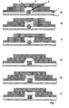
- Figure 1 shows different versions of the microcapillary according to claim 1 and Figure 2 is a sequential representation of the process steps for the production of the microcapillary.
- the anisotropic silicon structuring technology used to build up the microcapillary can also ensure that, depending on the application, the geometrically ideal design of the location microcapillary (1) - channel stopper (2) - membrane area (3) can be produced, as shown in FIG. 1 a) to f) is shown as an example.
- the three-dimensional geometric reproducibility of the microcapillary is limited solely by the lateral tolerances of the microelectronic technology for photolithography, which is + 3 ⁇ m.
- the microcapillary (1) constructed according to the invention and sealed with the glass pane (5) allows the integration of chemical microsensors with a differentiated constructional and material design.
- sequence (d) shows the integration of chemical microsensors as different as the front-side membrane ISFET (6), the rear-side membrane ISFET (7) and the microelectrode with bioactive membrane (8).
- the overall arrangement also performs electronic tasks.
- the wafer (4) containing the microcapillary carries on its insulated silicon top the conductor network (9) for the electronic connection between the chemical microsensors and the information technology periphery.
- the starting object for the realization of the microcapillary is a (100) silicon wafer (4) oxidized on both sides with 1.3 ⁇ m SiO 2 cover layers (10).
- a double-sided lithography process for producing the etching masks (11) is first carried out on this wafer, the later shaped piece of the microcapillary, and both SiO 2 cover layers (10) are structured.
- the SiO 2 cover layers (10) in turn then serve as an etching mask during the anisotropic structuring of the silicon wafer (4).
- the microcapillary is in an aqueous, alkaline KOH / 30% / 80 ° C etching solution in the silicon wafer (4) (1) anisotropically structured with the channel stoppers (2) and then the structured one Wafer (2) on its back with a Pyrex 7740 glass substrate (5) with a thickness of 130 ⁇ m connected to the sealed microcapillary by anodic bonding in the interface area (12).
- the defined opening of the fluid inlets or outlets (13) in the Pyrex glass substrate (5) takes place by hydrolytic etching in an alkaline bath at room temperature and 30 ... 40V DC voltage. After cleaning, a 1 ⁇ m thick interconnect metallization is deposited (9) made of aluminum, this metallization is structured photolithographically.
Landscapes
- Life Sciences & Earth Sciences (AREA)
- Chemical & Material Sciences (AREA)
- Health & Medical Sciences (AREA)
- Physics & Mathematics (AREA)
- Molecular Biology (AREA)
- Microelectronics & Electronic Packaging (AREA)
- Chemical Kinetics & Catalysis (AREA)
- Electrochemistry (AREA)
- Engineering & Computer Science (AREA)
- Analytical Chemistry (AREA)
- Biochemistry (AREA)
- General Health & Medical Sciences (AREA)
- General Physics & Mathematics (AREA)
- Immunology (AREA)
- Pathology (AREA)
- Micromachines (AREA)
Description
Die von H.H. Vlekkert, et al in [ Multi-Ion Sensing System Based on Glass-encapsulated pH-ISFETs and a Pseudo-REFET; Sensors and Actuators; B1 (1990)pp. 395-400 ] vorgestellte Multi-Ionen-Meßzelle besteht aus einer gläsernen Mikrokapillare. Diese wurde durch Stapeln zweier Glassubstrate aufgebaut, wovon eines einen kleinen Graben - die spätere Mikrokapillare besitzt und das zweite Löcher senkrecht auf die o.g. Kapillare beinhaltet, die den Zugang der Meßlösung an die empfindlichen Membrangebiete von aufgesetzten Mikrosensoren sichern sollen. Das Aufsetzen der ISFET-Mikosensoren auf das gelochte Glassubstrat erfolgt mittels anodischen Bondens. Auf diese Weise entstehen Sacklochverbindungen zwischen der Mikrokapillare und den empfindlichen Membrangebieten der ISFETs. Die Länge jedes der Sacklöcher beträgt 200µm. Diese Verfahrensweise beinhaltet drei sehr wesentliche Probleme. Das erste Problem resultiert aus der Art der Fluidankopplung über die Sacklöcher. Soll der integrierte chemische Mikrosensor einen Konzentrationssprung des in der Mikrokapillare strömenden Meßfluides erfassen, bedarf es zunächst einer Diffusionszeit für den Austausch des Fluides im Sackloch, dieser Vorgang benötigt Zeit und verzögert die Ansprechgeschwindigkeit und das Auflösungsvermögen der Meßanordnung. Ein zweites Problem ersteht daraus, daß alle in der Mikrokapillare entstehenden bzw. in diese einströmenden Gasbläschen in den Sacklöchern gesammelt und festgehalten werden. Dieser Umstand führt zu Fehlbenetzungen der empfindlichen Sensormembran und kann bis zum zeitlich befristeten Ausfall des Bauelementes eskalieren. Das dritte Problem besteht in der hohen elektrostatischen und thermischen Belastung der CMOS- Sensorbauelemente beim Montageprozeß des Mikrosensors in die Mikrozelle. Das zweite Realisierungsbeispiel von v.d.Schoot et al. [ A Modular Miniaturized Chemical Analysis System; Tech. Digest of the 4th. Int. Meet. Chemical Sensors; Tokyo; 13.-17. Sept. 19-92; pp. 394-397 ] nutzt ein fotopolymerisierbares Polymer zur Ausbildung einer Fließkapillare direkt auf einem Siliciumsubstrat mit monolitisch integrierten ISFETs. In diesem Beispiel sind Mikrokapillare und Sensorarray ein abgeschlossenes Bauelement, Sacklöcher treten hier nicht auf, Ausfälle eines Sensors ziehen jedoch das Auswechseln der Gesamtanordnung nach sich.
Mit der Erfindung wird die Mikrokapillare so konfiguriert, daß die in die Mikrokapillare integrierten chemischen Mikrosensoren, d.h. deren empfindliche Membrangebiete von dem zu analysierenden Meßfluid zwangsumspült und damit zwangsbenetzt werden. Diese Zwangsumspülung der Mikrosensoren innerhalb der Öffnungen wird konstruktiv durch Einführung sogenannter Kanalstopper realisiert, welche die Entstehung von Totvolumina minimieren.
Die erfindungsgemäße Mikrokapillare mit integrierten chemischen Mikrosensoren bietet dabei den Vorteil, daß unter Verwendung der Kanalstopper das Meßfluid auf optimale Weise zum Auftreffen auf das sensitive Gebiet des Sensors geführt wird, wodurch ein verbessertes Ansprechen im dynamischen Betrieb erreicht wird. Das erfindungsgemäße Verfahren bietet eine schonende Montage von Mikrosensoren unter Vermeidung hoher Temperatur- oder Spannungsbelastungen und gestattet darüberhinaus ein flexibles Auswechseln von Ausfallsensoren.
Die zum Aufbau der Mikrokapillare genutzte anisotrope Silicium-Strukturierungstechnologie kann darüber hinaus sichern, daß je nach Anwendungsfall die geometrisch ideale Gestaltung des Ortes Mikrokapillare (1) - Kanalstopper ( 2 )- Membrangebiet ( 3 ) herstellbar wird, wie dies in Fig. 1 a) bis f) beispielhaft dargestellt ist. Die dreidimensionale geometrische Reproduzierbarkeit der Mikrokapillare wird allein durch die lateralen Toleranzen der mikroelektronischen Technologie zur Fotolitografie begrenzt, diese liegt bei + 3 µm.
Die erfindungsgemäß aufgebaute, mit der Glasscheibe ( 5 ) abgedichtete Mikrokapillare ( 1) gestattet die Integration chemischer Mikrosensoren mit differenzierter konstruktiver und stofflicher Gestaltung. Das in Fig.2, Sequenz (d) dargestellte Ausführungsbeispiel zeigt die Integration von so unterschiedlichen chemischen Mikrosensoren wie dem Vorderseitenmembran-ISFET ( 6 ), dem Rückseitenmembran-ISFET ( 7 ) und der Mikroelektrode mit bioaktiver Membran ( 8 ). Neben den fluidtechnischen Funktionen der Mikrokapillare erfüllt die Gesamtanordnung auch elektronische Aufgaben. Der die Mikrokapillare enthaltende Wafer ( 4 ) trägt auf seiner isolierten Siliciumoberseite das Leiterzugnetzwerk ( 9 ) für die elektronische Verbindung zwischen den chemischen Mikrosensoren und die informationstechnische Peripherie.
Claims (3)
- Mikrokapillare (1) mit integrierten chemischen Mikrosensoren, bestehend aus einer in einem Wafer (4) mikrotechnisch strukturierten, ggfs. verzweigten oder gewendelten Kapillare (1) mit zusätzlichen, eine Verbindung zu den chemisch sensitiven Gebieten der Mikrosensoren herstellenden Öffnungen, dadurch gekennzeichnet, daß im Bereich dieser Öffnungen innerhalb der Kapillare (1) Kanalstopper (2) angeordnet sind, die in Form einer Strömungsumleitung eine Zwangsspülung der Mikrosensoren innerhalb der Öffnungen verursachen.
- Verfahren zur Herstellung einer Mikrokapillare (1) nach Anspruch 1, dadurch gekennzeichnet, daß in einem Siliziumwafer (4) durch einen zweiseitigen Strukturierungsprozeß der die spätere Kapillare (1) bildende Kanal einschließlich der Verbindungsöffnungen und der im Kanal stehenbleibenden Kanalstopper (2) ausgebildet werden, daß anschließend die den Mikrokanal tragende Seite des Wafers (4) mit einer Glasscheibe abgedeckt und die an die gegenüberliegende Oberfläche tretenden Öffnungen mit den Mikrosensoren abgedeckelt werden.
- Verfahren zur Herstellung einer Mikrokapillare (1) nach Anspruch 2, dadurch gekennzeichnet, daß die Montage der Mikrosensoren auf dem strukturierten Wafer (4) durch Reflowlöten mittels niedrig schmelzender Lote oder kaltaushärtender Klebstoffe erfolgt.
Applications Claiming Priority (2)
| Application Number | Priority Date | Filing Date | Title |
|---|---|---|---|
| DE4318407 | 1993-06-03 | ||
| DE4318407A DE4318407A1 (de) | 1993-06-03 | 1993-06-03 | Mikrokapillare mit integrierten chemischen Mikrosensoren und Verfahren zu ihrer Herstellung |
Publications (3)
| Publication Number | Publication Date |
|---|---|
| EP0633468A2 EP0633468A2 (de) | 1995-01-11 |
| EP0633468A3 EP0633468A3 (de) | 1996-08-21 |
| EP0633468B1 true EP0633468B1 (de) | 1999-08-25 |
Family
ID=6489515
Family Applications (1)
| Application Number | Title | Priority Date | Filing Date |
|---|---|---|---|
| EP94108169A Expired - Lifetime EP0633468B1 (de) | 1993-06-03 | 1994-05-27 | Mikrokapillare mit integrierten chemischen Mikrosensoren und Verfahren zu ihrer Herstellung |
Country Status (2)
| Country | Link |
|---|---|
| EP (1) | EP0633468B1 (de) |
| DE (2) | DE4318407A1 (de) |
Cited By (2)
| Publication number | Priority date | Publication date | Assignee | Title |
|---|---|---|---|---|
| US6017496A (en) | 1995-06-07 | 2000-01-25 | Irori | Matrices with memories and uses thereof |
| US6329139B1 (en) | 1995-04-25 | 2001-12-11 | Discovery Partners International | Automated sorting system for matrices with memory |
Families Citing this family (15)
| Publication number | Priority date | Publication date | Assignee | Title |
|---|---|---|---|---|
| US5872010A (en) * | 1995-07-21 | 1999-02-16 | Northeastern University | Microscale fluid handling system |
| US6136274A (en) * | 1996-10-07 | 2000-10-24 | Irori | Matrices with memories in automated drug discovery and units therefor |
| GB9808890D0 (en) | 1998-04-28 | 1998-06-24 | Dow Corning | Silicone coated textile fabrics |
| US6245227B1 (en) | 1998-09-17 | 2001-06-12 | Kionix, Inc. | Integrated monolithic microfabricated electrospray and liquid chromatography system and method |
| CN100525876C (zh) | 1998-09-17 | 2009-08-12 | 阿德文生物系统公司 | 产生液体电喷射的方法 |
| DE19850041A1 (de) * | 1998-10-30 | 2000-05-04 | Festo Ag & Co | Mikrotechnologisches Bondverfahren und zugehörige Vorrichtung |
| US6633031B1 (en) | 1999-03-02 | 2003-10-14 | Advion Biosciences, Inc. | Integrated monolithic microfabricated dispensing nozzle and liquid chromatography-electrospray system and method |
| CA2395694C (en) | 1999-12-30 | 2006-11-21 | Advion, Inc. | Multiple electrospray device, systems and methods |
| US6596988B2 (en) | 2000-01-18 | 2003-07-22 | Advion Biosciences, Inc. | Separation media, multiple electrospray nozzle system and method |
| WO2002038490A2 (de) | 2000-11-07 | 2002-05-16 | GeSIM Gesellschaft für Silizium-Mikrosysteme mbH | Verfahren zum herstellen von glas-silizium-glas sandwichstrukturen |
| US6649078B2 (en) | 2000-12-06 | 2003-11-18 | The Regents Of The University Of California | Thin film capillary process and apparatus |
| US7235389B2 (en) | 2001-04-23 | 2007-06-26 | Samsung Electronics Co., Ltd. | Molecular detection device and chip including MOSFET |
| DE10206464A1 (de) * | 2002-02-16 | 2003-08-28 | Micronas Gmbh | Verfahren zur Herstellung einer Sensor- oder Aktuatoranordnung sowie Sensor- oder Aktuatoranordnung |
| DE10257097B4 (de) * | 2002-12-05 | 2005-12-22 | X-Fab Semiconductor Foundries Ag | Verfahren zur Herstellung von mikroelektromechanischen Systemen (Microelectromechanical Systems: MEMS) mittels Silizium-Hochtemperatur-Fusionsbonden |
| GB0306163D0 (en) | 2003-03-18 | 2003-04-23 | Univ Cambridge Tech | Embossing microfluidic sensors |
Family Cites Families (8)
| Publication number | Priority date | Publication date | Assignee | Title |
|---|---|---|---|---|
| DK144107C (da) * | 1975-10-15 | 1982-05-17 | Radiometer As | Maalekammerenhed til et elektrokemisk maaleapparat og fremgangsmaade til fremstilling af maalekammerenheden |
| US4627893A (en) * | 1984-03-28 | 1986-12-09 | Amdev, Inc. | Means and methods for quantitative determination of analyte in liquids |
| GB8522785D0 (en) * | 1985-09-14 | 1985-10-16 | Emi Plc Thorn | Chemical-sensitive semiconductor device |
| JPS63278236A (ja) * | 1987-02-18 | 1988-11-15 | Mitsubishi Electric Corp | 半導体装置 |
| US4808260A (en) * | 1988-02-05 | 1989-02-28 | Ford Motor Company | Directional aperture etched in silicon |
| US5132012A (en) * | 1988-06-24 | 1992-07-21 | Hitachi, Ltd. | Liquid chromatograph |
| JPH02143466A (ja) * | 1988-11-25 | 1990-06-01 | Mitsubishi Electric Corp | 半導体装置の製造方法 |
| JP3001104B2 (ja) * | 1989-10-04 | 2000-01-24 | オリンパス光学工業株式会社 | センサー構造体及びその製造法 |
-
1993
- 1993-06-03 DE DE4318407A patent/DE4318407A1/de not_active Withdrawn
-
1994
- 1994-05-27 EP EP94108169A patent/EP0633468B1/de not_active Expired - Lifetime
- 1994-05-27 DE DE59408651T patent/DE59408651D1/de not_active Expired - Fee Related
Cited By (2)
| Publication number | Priority date | Publication date | Assignee | Title |
|---|---|---|---|---|
| US6329139B1 (en) | 1995-04-25 | 2001-12-11 | Discovery Partners International | Automated sorting system for matrices with memory |
| US6017496A (en) | 1995-06-07 | 2000-01-25 | Irori | Matrices with memories and uses thereof |
Also Published As
| Publication number | Publication date |
|---|---|
| DE59408651D1 (de) | 1999-09-30 |
| DE4318407A1 (de) | 1994-12-08 |
| EP0633468A2 (de) | 1995-01-11 |
| EP0633468A3 (de) | 1996-08-21 |
Similar Documents
| Publication | Publication Date | Title |
|---|---|---|
| EP0633468A2 (de) | Mikrokapillare mit integrierten chemischen Mikrosensoren und Verfahren zu ihrer Herstellung | |
| DE10060433B4 (de) | Verfahren zur Herstellung eines Fluidbauelements, Fluidbauelement und Analysevorrichtung | |
| DE60023464T2 (de) | Verfahren zur Herstellung integrierter chemischer Mikroreaktoren aus Halbleitermaterial sowie integrierter Mikroreaktor | |
| DE60215962T2 (de) | Flexible Konstruktion mit integriertem Sensor/stellglied | |
| DE60223193T2 (de) | Herstellung von integrierten fluidischen Vorrichtungen | |
| EP0538428B1 (de) | Verfahren zur herstellung von miniaturisierten chemo- und biosensorelementen mit ionenselektiver membran sowie von trägern für diese elemente | |
| DE19619921B4 (de) | Verfahren zum Herstellen einer Halbleitervorrichtung mit Funktionselement und Schutzkappe | |
| DE69423010T2 (de) | Methode zur erzeugung von hohlraumstrukturen | |
| DE112014000923B4 (de) | Mikrofluidchip mit dielektrophoretischen Elektroden, die sich in einem hydrophilen Fließweg erstrecken | |
| DE60018473T2 (de) | Vorrichtung und verfahren zur ausführung elektrischer messungen an gegenständen | |
| DE69424557T2 (de) | Druckwandler mit aufgehangter membran | |
| EP2394156B1 (de) | Anordnung und verfahren zum elektrochemischen messen von biochemischen reaktionen sowie herstellungsverfahren der anordnung | |
| EP1144976B1 (de) | Verfahren zum erzeugen einer mikromechanischen struktur für ein mikro-elektromechanisches element | |
| DE4415984A1 (de) | Halbleitersensor mit Schutzschicht | |
| DE69528218T2 (de) | Flüssigkeitseigenschaftsfühler mit metallplattierten Ringen für verbessertes Packaging | |
| EP0961921A2 (de) | Thermischer membransensor und verfahren zu seiner herstellung | |
| DE19600400C2 (de) | Mikromechanisches Bauteil mit planarisiertem Deckel auf einem Hohlraum und Herstellverfahren | |
| DE4031425A1 (de) | Fet-sensorvorrichtung vom flusszellenadaptiv-typ und herstellungsverfahren | |
| DE102010002915A1 (de) | Mikrofluidischer Sensor | |
| DE19710358C2 (de) | Mikrostrukturierter Sensor | |
| EP1144977B1 (de) | Verfahren zum erzeugen eines mikro-elektromechanischen elements | |
| EP1382952A1 (de) | Mikromechanischer Druckgeber mit Sensor an Trennmembran des Gehäuses | |
| DE102008005350B4 (de) | Mikrofluidische Vorrichtungen mit Nanokanälen | |
| DE19929264A1 (de) | Universaltransducer | |
| DE10257097B4 (de) | Verfahren zur Herstellung von mikroelektromechanischen Systemen (Microelectromechanical Systems: MEMS) mittels Silizium-Hochtemperatur-Fusionsbonden |
Legal Events
| Date | Code | Title | Description |
|---|---|---|---|
| PUAI | Public reference made under article 153(3) epc to a published international application that has entered the european phase |
Free format text: ORIGINAL CODE: 0009012 |
|
| AK | Designated contracting states |
Kind code of ref document: A2 Designated state(s): BE DE ES FR GB NL |
|
| PUAL | Search report despatched |
Free format text: ORIGINAL CODE: 0009013 |
|
| AK | Designated contracting states |
Kind code of ref document: A3 Designated state(s): BE DE ES FR GB NL |
|
| 17P | Request for examination filed |
Effective date: 19970207 |
|
| GRAG | Despatch of communication of intention to grant |
Free format text: ORIGINAL CODE: EPIDOS AGRA |
|
| 17Q | First examination report despatched |
Effective date: 19981006 |
|
| GRAG | Despatch of communication of intention to grant |
Free format text: ORIGINAL CODE: EPIDOS AGRA |
|
| GRAH | Despatch of communication of intention to grant a patent |
Free format text: ORIGINAL CODE: EPIDOS IGRA |
|
| GRAH | Despatch of communication of intention to grant a patent |
Free format text: ORIGINAL CODE: EPIDOS IGRA |
|
| GRAA | (expected) grant |
Free format text: ORIGINAL CODE: 0009210 |
|
| RIN1 | Information on inventor provided before grant (corrected) |
Inventor name: FIEHN, HENDRIK Inventor name: PHAM, MINH TAN, DR. Inventor name: HOWITZ, STEFFEN, DR. |
|
| AK | Designated contracting states |
Kind code of ref document: B1 Designated state(s): BE DE ES FR GB NL |
|
| PG25 | Lapsed in a contracting state [announced via postgrant information from national office to epo] |
Ref country code: NL Free format text: LAPSE BECAUSE OF FAILURE TO SUBMIT A TRANSLATION OF THE DESCRIPTION OR TO PAY THE FEE WITHIN THE PRESCRIBED TIME-LIMIT Effective date: 19990825 Ref country code: GB Free format text: LAPSE BECAUSE OF FAILURE TO SUBMIT A TRANSLATION OF THE DESCRIPTION OR TO PAY THE FEE WITHIN THE PRESCRIBED TIME-LIMIT Effective date: 19990825 Ref country code: FR Free format text: LAPSE BECAUSE OF FAILURE TO SUBMIT A TRANSLATION OF THE DESCRIPTION OR TO PAY THE FEE WITHIN THE PRESCRIBED TIME-LIMIT Effective date: 19990825 Ref country code: ES Free format text: THE PATENT HAS BEEN ANNULLED BY A DECISION OF A NATIONAL AUTHORITY Effective date: 19990825 |
|
| REF | Corresponds to: |
Ref document number: 59408651 Country of ref document: DE Date of ref document: 19990930 |
|
| EN | Fr: translation not filed | ||
| NLV1 | Nl: lapsed or annulled due to failure to fulfill the requirements of art. 29p and 29m of the patents act | ||
| GBV | Gb: ep patent (uk) treated as always having been void in accordance with gb section 77(7)/1977 [no translation filed] |
Effective date: 19990825 |
|
| PG25 | Lapsed in a contracting state [announced via postgrant information from national office to epo] |
Ref country code: BE Free format text: LAPSE BECAUSE OF NON-PAYMENT OF DUE FEES Effective date: 20000531 |
|
| PLBE | No opposition filed within time limit |
Free format text: ORIGINAL CODE: 0009261 |
|
| STAA | Information on the status of an ep patent application or granted ep patent |
Free format text: STATUS: NO OPPOSITION FILED WITHIN TIME LIMIT |
|
| 26N | No opposition filed | ||
| BERE | Be: lapsed |
Owner name: FORSCHUNGSZENTRUM ROSSENDORF E.V. Effective date: 20000531 |
|
| PGFP | Annual fee paid to national office [announced via postgrant information from national office to epo] |
Ref country code: DE Payment date: 20050622 Year of fee payment: 12 |
|
| PG25 | Lapsed in a contracting state [announced via postgrant information from national office to epo] |
Ref country code: DE Free format text: LAPSE BECAUSE OF NON-PAYMENT OF DUE FEES Effective date: 20061201 |